

Page 1

查询MB4072供应商
FUJITSU SEMICONDUCTOR
DATA SHEET
LINEAR IC
1 CHANNEL 8-BIT D/A
CONVERTER
MB4072
1 CHANNEL 8-BIT D/A CONVERTER
The Fujitsu MB4072 is a High-Speed Digital to Analog Converter IC. The
MB4072’s current outputs are high impedance open-collector, which provide
voltage output w ith a load or current t o voltage conv erter for various applications
with operational amplifiers, microcomputers, etc.
Threshold level of digital inputs is variable with the level control input for various
interface level.
• Settling Time : 85ns
• Linearity Error : ±0.19%max.
• Full-scal e Temperature coefficient: ±10ppm/°C typ.
• Output Voltage Compliance : -10V to +18V
• Multiplying Operation
• True/Complimentary Current Sink Output
• Adjustable Threshold Level of Digital Inputs :Interface directly with
TTL, CMOS, ECL, etc.
• Wide Supply Voltage Range : ±4.5V to ±18V
• Low Power Consumption : 33mW at ±5V typ.
• Operation Temperature : -40°C to +85°C
• Compatible with DAC-08
• Package : Plastic DIP Package: (Suffix: -P)
Plastic FPT Package: (Suffix: -PF)
DS04-13200-3E
PLASTIC PACKAGE
DIP-16P-M04
PLASTIC PACKAGE
FPT-16P-M06
PIN ASSIGNMENT
■ ABSOLUTE MAXIMUM RATINGS
(TA =25°C)
Parameter Symbol Value Unit
Supply Voltage V+ to V- 37 V
Digital Input Voltage VI V- to V- +37 V
Threshold Control Voltage VLC V- to V+ V
Reference Input Voltage
Differential Reference Input
Voltage
Reference Input Current IREF 5 mA
Power Consumption PD 500 mW
Storage Temp. TSTG -55 to +125 °C
NOTE: Permanent device damage may occur if the above Absolute Maximum
Ratings are exceeded. Functional operation should be restricted to the
conditions as detailed in the operational sections of this data sheet. Exposure
to absolute maximum rating conditions for extended periods may affect de vice
reliability .
VREF(+) V- to V+ V
VREF(-) V- to V+ V
VREF(+) to VREF(-) ±18.5 V
COMP
VLC
IOUT
IOUT
(MSB)B1
This device contains circuitry to protect the inputs against
damage due to high static volta ges or electric fields. How ever ,
it is advised that normal precautions be taken to avoid
application of any voltage higher than maxim um rated voltages
to this high impedance circuit.
V-
B2
B3
B4
1
2
3
4
TOP VIEW
5
6
7
8
16
15
14
13
12
11
10
9
V
REF(-)
VREF(+)
V+
B8(LSB)
B7
B6
B5
1
Page 2
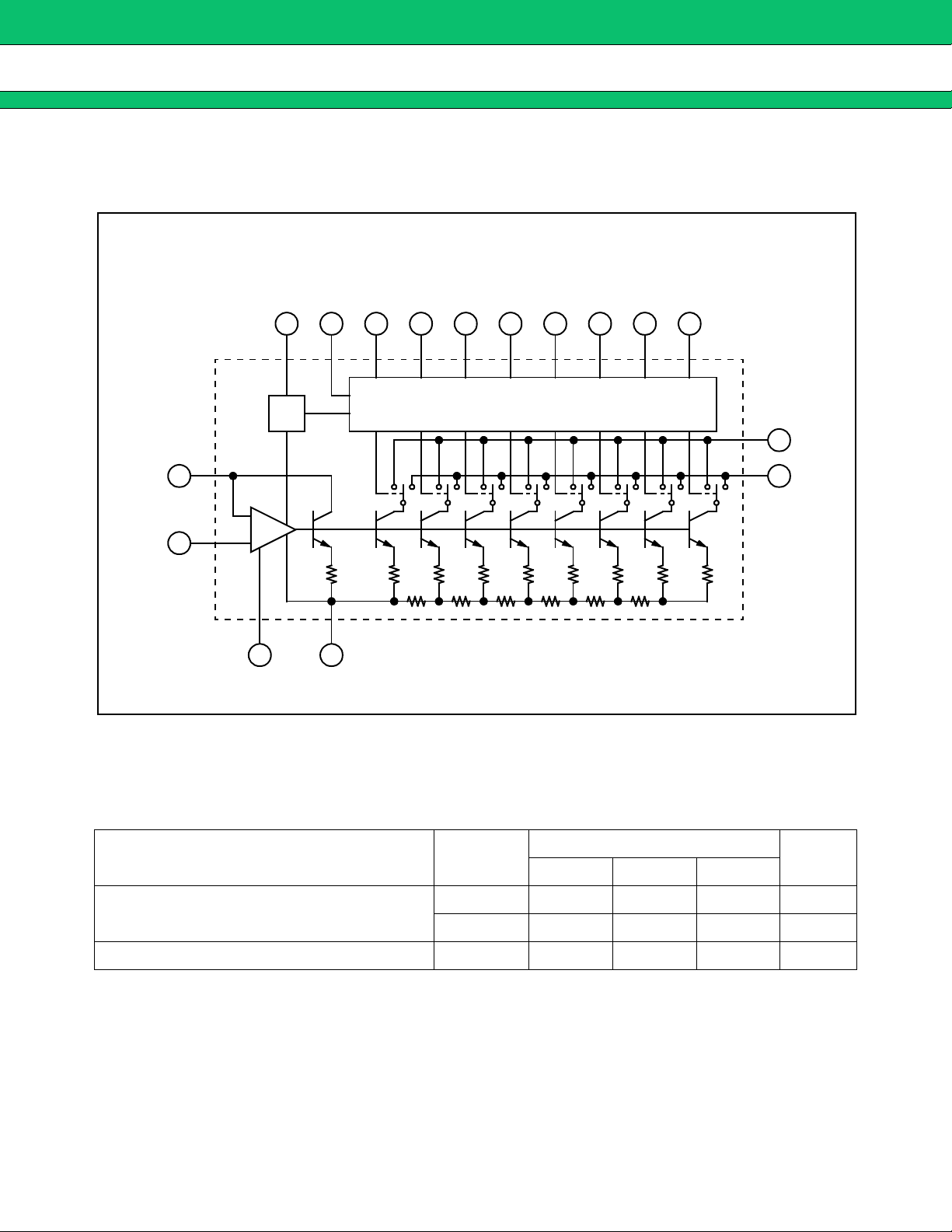
MB4072
BIAS
NETWORK
V+ V
Fig. 1 - BLOCK DIAGRAM
MSB LSB
LC B1 B2 B3 B4 B5 B6 B7 B8
113 5 6 7 8 9 10 11 12
INTERFACE LEVEL CONTROL CIRCUIT
4
IOUT
___
214
IOUTVREF(+)
CURRENT
SW.
V
-
VREF(-)
15
+
-
REF
Amp
16 3
COMP
■ RECOMMENDED OPERATING CONDITIONS
Parameter Symbol Unit
V+ +4.5 - +18 V
Supply Voltage
V- -18 - -4.5 V
Operating Temperature TA -40 - +85 °C
Min Typ Max
2
Page 3
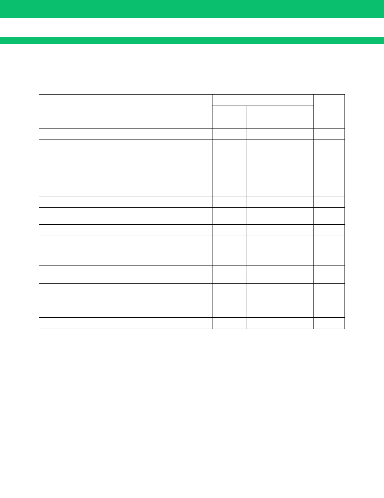
■ ELECTRICAL CHARACTERISTICS
(Recommended Operating Conditions unless otherwise noted.)
(V+ = +15V, V- = -15V, IREF = 2.0mA, TA = -40°C to +85°C )
MB4072
Parameter Symbol
Resolution 8 8 8 bits
Monotonicity 8 8 8 bits
Linearity Error LE - - ±0.19 % (FSR)
Settling Time (Final Value: ±1/2 LSB, TA=25°C, On/Off
Switching for Each bit/All bits)
Propagation Delay Time (TA=25°C, On/Off Switching for
Each bit/All bits)
Temperature coefficient at full-scale TCIFS - ±10 ±50 ppm/°C
Output Voltage Range (∆IFS 1/2 LSB, ROUT 20MΩ typ.) VOC -10 - +18 V
Output Current at full-scale (VREF=10.000V, R14=5.000kΩ,
R15=5.000kΩ, T
Symmetry at full-scale (IFSS=IFS4-IFS2) TFSS - ±1.0 ±8.0 µA
Output Current at zero scale IZS - 0.2 2.0 µA
Output Current Range (R14=5.000kΩ, R15=5.000kΩ,
V
REF=+15.0V, V-=-10V)
Output Current Range (R14=5.000kΩ, R15=5.000kΩ,
V
REF=+25.0V, V-=-12V)
A=25°C)
tS - 85 150 ns
tPLH
tPHL
IFS4 1.94 1.99 2.04 mA
IOR1 2.1 - - mA
IOR2 4.2 - - mA
Min Typ Max
- 35 60 ns
Value
Unit
Low-level Input Voltage (VLC=0V) VIL - - 0.8 V
High-level Input Voltage (VLC=0V) VIH 2.0 - - V
Low-level Input Current (VLC=0V, VIN=-10V to +0.8V) IIL - -0.2 -10 µA
High-level Input Current (VLC=0V, VIN=2.0V to 18V) IIH - 0.002 10 µA
3
Page 4

MB4072
■ ELECTRICAL CHARACTERISTICS (Continued)
(VS=±15V, IREF = 2.0mA, TA = -40°C to +85°C)
Parameter Symbol
Logic Input Voltage Range (V-=-15V)
Logic Threshold Voltage Range (V+=+15V, V-=-15V)
Reference Bias Current I15 - -1.0 -3.0 µA
Reference Input Through Rate (REQ=200Ω, RL=100Ω, CL=0pF)
Supply Voltage Sensitivity* (V+=+4.5V to +18V, IREF=1mA)
Supply Voltage Sensitivity* (V-=-4.5V to -18V, IREF=1mA)
)
Supply Current
(V-=+5V, V-=-5V, IREF=1.0mA
(V+=+5V, V-=-15V, IREF=2.0mA)
(V+=+15V, V-=-15V, IREF=2.0mA)
VIS -10 - +18 V
VTHR
dl
dt
PSSIFS+ - ±0.0003 ±0.01 %/%
PSSIFS- - ±0.002 ±0.01 %/%
I-
I-
I-
I-
I-
I-
Min Typ Max
-10 - +13.5 V
4.0 8.0 - mA/µs
- 2.3 3.8 mA
- -4.3 -5.8 mA
- 2.4 3.8 mA
- -6.4 -7.8 mA
- 2.5 3.8 mA
- -6.5 -7.8 mA
Value
Unit
(V+=+5V, V-=-5V, IREF=1.0mA)
Power Dissipation
*Note: PSSIFS=( x 100) / ( x 100)
(V+=+5V, V-=-15V, IREF=2.0mA)
(V+=+15V, V-=-15V, IREF=2.0mA)
∆IFS
____
IFS
18-4.5
_______
15
PD - 33 48 mW
PD - 103 136 mW
PD - 135 174 mW
4
Page 5

Fig. 2 - WAVEFORM SYNTHESIZER
Pattern
Generator
MB4072
+10V
2mA
5kΩ
5kΩ
14
15
5 to 12
MB4072
IO
__
IO
5kΩ
5kΩ
-
+
OUT
V
4
2
5
Page 6

MB4072
■ PACKAGE DIMENSIONS
16-LEAD PLASTIC DUAL IN-LINE PACKAGE
(Case No.: DIP-16P-M04)
INDEX-1
INDEX-2
+.012
.039
-0
+0.30
(0.99 )
-0
.050(1.27)
MAX
.770
.100(2.54)
+.008
-.012
TYP
+0.20
(19.55 )
-0.30
.060
(1.52 )
+.012
-0
+0.30
-0
.018
(0.46
±.003
±0.08)
±.010
.244
±0.25)
(6.20
.172(4.36)MAX
.118(3.00)MIN
.020(0.51)MIN
.300(7.62)
TYP
.010
(0.25
±.002
±0.05)
15
°MAX
1991 FUJITSU LIMITED D16033S-2C
Dimensions in
inches (millimeters)
6
Page 7

■ PACKAGE DIMENSIONS (Continued)
16-LEAD PLASTIC FLAT PACKAGE
(Case No.: FPT-16P-M06 )
.050(1.27)
TYP
.400
INDEX
+.010
-.008
+0.25
(10.15 )
-0.20
±.004
.018
(0.45
±0.10)
“B”
.209
(5.30
Ø.005(0.13)
(7.80
±.012
±0.30)
M
.307
±.016
±0.40)
MB4072
.089(2.25)MAX
(MOUNTING HEIGHT)
.002(0.05)MIN
(STAND OFF HEIGHT)
.268
+.016
-.008
.006
+0.40
(6.80 )
-0.20
±.008
.020
±0.20)
(0.50
+.002
(0.15 )
-.001
+0.05
-0.02
.004(0.10)
.350(8.89) REF
1991 FUJITSU LIMITED F16015S-2C
“A”
Details of “A” part
.016(0.40)
.008(0.20)
.007(0.18)
MAX
.027(0.68)
MAX
Details of “B” part
.006(0.15)
.008(0.20)
.007(0.18)
MAX
.027(0.68)
MAX
Dimensions in
inches (millimeters)
7
Page 8

MB4072
FUJITSU LIMITED
For further information please contact:
Japan
FUJITSU LIMITED
Corporate Global Business Support Division
Electronic Devices
KAWASAKI PLANT, 1015, Kamikodanaka
Nakahara-ku, Kawasaki-shi
Kanagawa 211, Japan
Tel: (044) 754-3753
Fax: (044) 754-3329
North and South America
FUJITSU MICROELECTRONICS, INC.
Semiconductor Division
3545 North First Stree t
San Jose, CA 95134-1804, U.S.A.
Tel: (408) 922-9000
Fax: (408) 432-9044/9045
Europe
FUJITSU MIKROELEKTRONIK GmbH
Am Siebenstein 6-10
63303 Dreieich-Buchschlag
Germany
Tel: (06103) 690-0
Fax: (06103) 690-122
Asia Pacific
FUJITSU MICROELECTRONICS ASIA PTE. LIMITED
No . 51 Bras Basah Road,
Plaza By The Park,
#06-04 to #06-07
Singapore 189554
Tel: 336-1600
Fax: 336-1609
All Rights Reserved.
Circuit diagrams utilizing Fujitsu products are included as a
means of illustrating typical semiconductor applications.
Complete information sufficient for construction purposes is not
necessarily given.
The information contained in this document has been carefully
checked and is believed to be reliable. However, Fujitsu
assumes no responsibility for inaccuracies.
The information containe d in this document doe s not convey any
license under the copyrights, patent rights or trademarks claimed
and owned by Fujitsu.
Fujitsu reserves the right to change products or specifications
without notice.
No part of this publ icati on may b e copi ed or re produc ed in an y
form or by any mean s, or tr ansferr ed to any thir d part y with out
prior written consent of Fujitsu.
The information contained in this docum ent are not inte nded for
use with equipments which require extremely high reliability
such as aerospace equipments, undersea repeaters, nuclear
control systems or medical equipments for life support.
F9601
FUJITSU LIMITED Printed in Japan
8
 Loading...