

Page 1
FUJITSU SEMICONDUCTOR
DATA SHEET
DS04-21340-2E
ASSP
Single Serial Input
PLL Frequency Synthesizer
On-Chip 1.2 GHz Prescaler
MB15E03
■
DESCRIPTION
The Fujitsu MB15E03 is serial input Phase Locked Loop (PLL) frequency synthesizer with a 1.2 GHz prescaler. A
64/65 or a 128/129 can be selected for the prescaler that enables pulse swallow operation.
The latest BiCMOS process technology is used, resuItantly a supply current is limited as low as 3.5 mA typ. This
operates with a supply voltage of 3.0 V (typ.).
Furthermore, a super charger circuit is included to get a fast tuning as well as low noise performance. As a result
of this, MB15E03 is ideally suitable for digital mobile communications, such as GSM (Global System for Mobile
Communications).
■
FEATURES
• High frequency operation: 1.2 GHz max
• Low power supply voltage: VCC = 2.7 to 3.6 V
• Very Low power supply current : I
• Power saving function : I
• Pulse swallow function: 64/65 or 128/129
• Serial input 14-bit programmable reference divider: R = 5 to 16,383
• Serial input 18-bit programmable divider consisting of:
- Binary 7-bit swallow counter: 0 to 127
- Binary 11-bit programmable counter: 5 to 2,047
• Wide operating temperature: Ta = –40 to 85°C
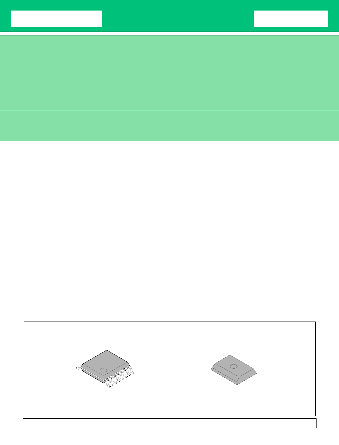
• Plastic 16-pin SSOP package (FPT-16P-M05) and 16-pin BCC package (LCC-16P-M02)
■
PACKAGES
16-pin, Plastic SSOP
= 0.1 µA typ.
PS
= 3.5 mA typ. (VCC = 3 V)
CC
16-pin, Plastic BCC
(FPT-16P-M05)
This device contains circuitry to protect the inputs against damage due to high static voltages or electroc fields. How e v er, it is advised that normal precautions
be taken to avoid application of any voltage higher than maximum rated voltages to this high impedance circuit.
(LCC-16P-M02)
Page 2
MB15E03
■
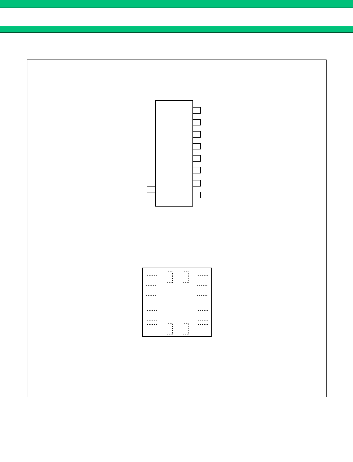
PIN ASSIGNMENTS
SSOP-16 pin
BCC-16 pin
OSCin
OSCout
Vp
Vcc
Do
GND
Xfin
fin
OSCout
V
CC
V
Do
GND
Xfin
(FPT-16P-M05)
OSCin φR
1
P
2
3
4
5
6
1
2
3
4
TOP
VIEW
5
6
7
8
16 15
TOP
VIEW
78
16
15
14
13
12
11
10
φR
φP
LD/fout
ZC
PS
LE
Data
9
Clock
14
φP
13
LD/fout
12
ZC
11
PS
10
LE
9
Data
fin Clock
(LCC-16P-M02)
2
Page 3
■
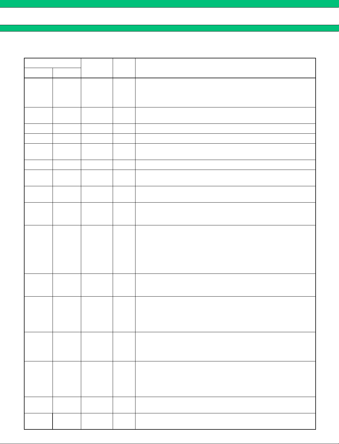
PIN DESCRIPTIONS
MB15E03
Pin no.
SSOP BCC
Pin
name
I/O Descriptions
Programmable reference divider input.
Oscillator input.
1 16 OSC
IN
I
Connection for an crystal or a TCXO.
TCXO should be connected with a coupling capacitor.
2 1 OSC
32V
OUT
P
Oscillator output.
O
Connection for an external crystal.
– Power supply voltage input for the charge pump.
43VCC– Power supply voltage input.
54D
O
Charge pump output.
O
Phase of the charge pump can be reversed by FC bit.
6 5 GND – Ground.
7 6 Xfin I
8 7 fin I
Prescaler complementary input, and should be grounded via a
capacitor.
Prescaler input.
Connection with an external VCO should be done with AC coupling.
Clock input for the 19-bit shift register.
9 8 Clock I
Data is shifted into the shift register on the rising edge of the clock.
(Open is prohibited.)
Serial data input using binary code.
The last bit of the data is a control bit.
Control bit = ”H” ; Data is transmitted to the programmable
10 9 Data I
reference
counter.
Control bit = ”L” ; Data is transmitted to the programmable
counter.
Load enable signal input
11 10 LE I
When LE is high, the data in the shift register is transferred to a
latch, according to the control bit in the serial data.
Power saving mode control. This pin must be set at ”L” at PowerON.
12 11 PS I
(Open is prohibited.)
PS = ”H” ; Normal mode
PS = ”L” ; Power saving mode
Forced high-impedance control for the charge pump (with internal
13 12 ZC I
pull up resistor.)
ZC = ”H” ; Normal Do output.
ZC = ”L” ; Do becomes high impedance.
Lock detect signal output(LD)/phase comparator monitoring
output (fout).
14 13 LD/fout O
The output signal is selected by LDS bit in the serial data.
LDS = ”H” ; outputs fout (fr/fp monitoring output)
LDS = ”L” ; outputs LD (”H” at locking, ”L” at unlocking.)
15 14
16 15
φ
PO
φ
RO
Phase comparator output for an external charge pump. Nch open
drain output.
Phase comparator output for an external charge pump. CMOS
output.
(Open is prohibited.)
(Open is prohibited.)
3
Page 4
MB15E03
■
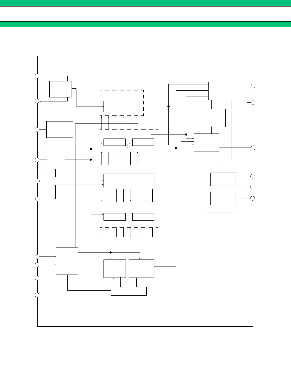
BLOCK DIAGRAM
1
OSCIN
Crystal
Oscillator
circuit
OSCOUT
2
Intermittent
12
11
10
mode control
(power save)
1-bit
control
latch
PS
LE
Data
Programmable
reference divider
Binary 14-bit
reference counter
17-bit latch
14-bit latch 3-bit latch
LE
19-bit shift register
C
N
19-bit shift register
T
SW
LDS
FC
fr
fp
fr
LD/fr/fp
selector
fp
comparator
LD
Lock
detector
Phase
Charge
pump
16
15
14
13
3
φR
φP
LD/fout
ZC
VP
Clock
XfIN
GND
VCC
9
7-bit latch
18-bit latch
11-bit latch
LE
SW
Super
charger
DO
5
Programmable divider
7
fIN
8
6
4
Prescaler
64/65,
128/129
MD
Binary 7-bit
swallow
counter
Control Cir-
Binary 11-bit
programma-
ble counter
fp
Note: SSOP-16 pin
4
Page 5
MB15E03
■
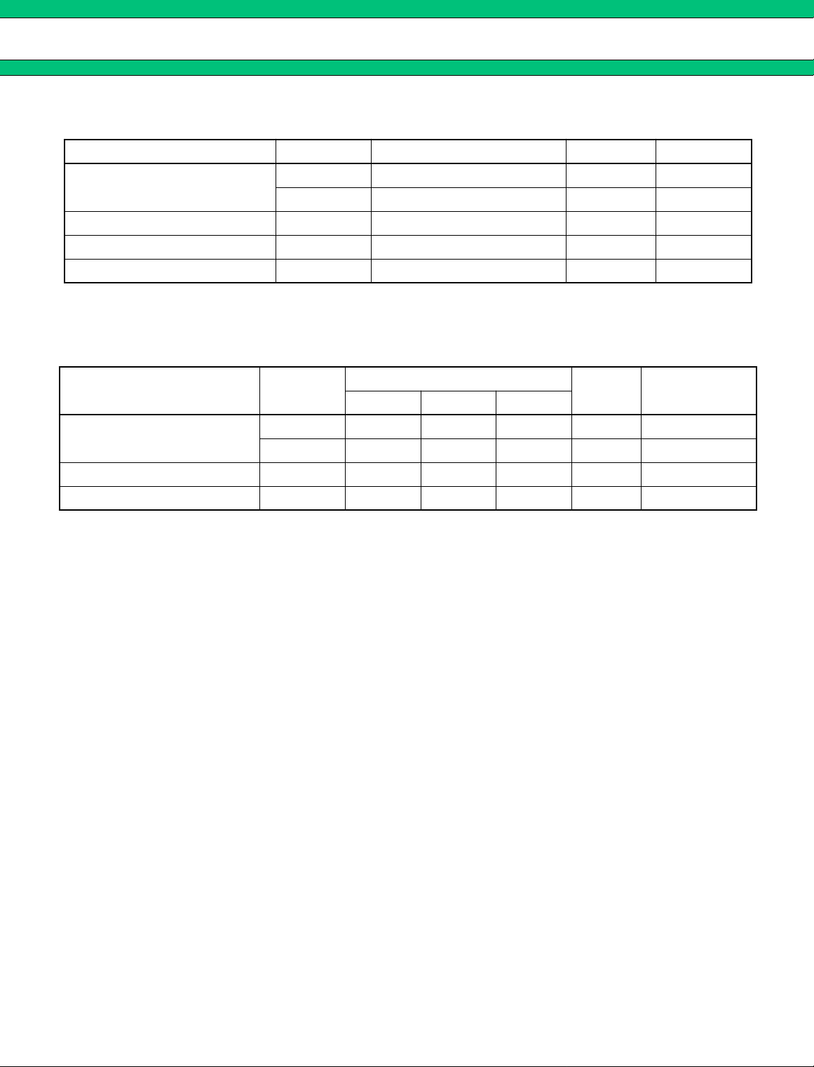
ABSOLUTE MAXIMUM RATINGS
Parameter Symbol Rating Unit Remark
V
CC
Power supply voltage
V
P
Input voltage V
Output voltage V
Storage temperature T
I
O
stg
WARNING: Semiconductor devices can be permanently damaged by application of stress (voltage, current,
temperature, etc.) in excess of absolute maximum ratings. Do not exceed these ratings.
■
RECOMMENDED OPERATING CONDITIONS
–0.5 to +4.0 V
VCC to +6.0 V
–0.5 to VCC +0.5 V
–0.5 to VCC +0.5 V
–55 to +125
°
C
Parameter Symbol
Unit Remark
Min. Typ. Max.
Value
V
CC
2.7 3.0 3.6 V
Power supply voltage
V
P
Input voltage V
I
Operating temperature Ta –40 – +85
V
CC
– 6.0 V
GND – V
CC
V
°
C
WARNING: Recommended operating conditions are nor mal operating ranges for the semiconductor device. All
the device’s electrical characteristics are warranted when operated within these ranges.
Always yse semiconductor devices within the recommended operating conditions. Operation outside
these ranges may adversely affect reliability and could result in device failure.
No warranty is made with repect to uses, operating conditions, or combinations not represented on
the data sheet. Users considering application outside the listed conditions are advised to contact their
FUJITSU representative beforehand.
5
Page 6
MB15E03
■
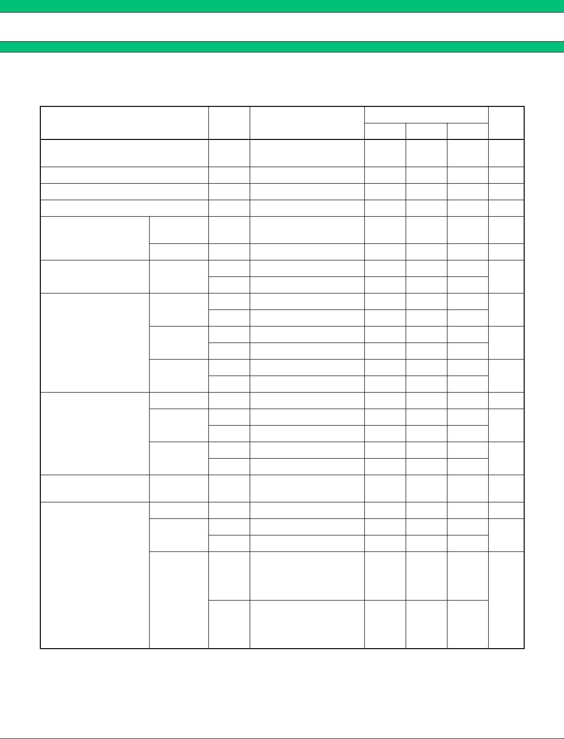
ELECTRICAL CHARACTERISTICS
(VCC = 2.7 to 3.6 V, Ta = –40 to +85°C)
0.7
Value
0.1
*2
10
CC
––
Vcc
×
0.3
––
––
Unit
mVp-p
mA
mA
Parameter Symbol Condition
Min. Typ. Max.
Power supply current*
1
Power saving current Ips
fin = 1200 MHz,
I
CC
fosc = 12 MHz
PS = “L”, ZC = ”H” or open
– 3.5 – mA
–
Operating frequency fin 100 – 1200 MHz
Crystal oscillator operating frequency
fin Vfin
Input sensitivity
OSCin V
Input voltage
Data, Clock,
LE, PS, ZC
Data, Clock,
LE, PS
Input current
ZC
f
V
min. 500 mVp-p 3 – 40 MHz
50 Ω system
(Refer to the test circuit.)
OSC
IH
V
IL
I
IH
IL
I
I
IH
IL
I
Pull up input –100 – 0
IH
I
–10 – +2 dBm
500 – V
Vcc
×
––
–1.0 – +1.0
–1.0 – +1.0
–1.0 – +1.0
0 – +100
OSC
OSCin
I
Output voltage
IL
φ
PV
φ
R,
LD/fout
OL
OH
V
V
OL
DOH
V
Open drain output – – 0.4 V
VCC = 3 V, IOH = –1 mA
VCC = 3 V, IOL = 1 mA – – 0.4
VCC = 3 V, I
DOH
= –1 mA
–100 – 0
Vcc – 0.4
Vp – 0.4
Do
High impedance
cutoff current
DOL
V
Do I
φ
PI
φ
R,
LD/fout
VCC = 3 V, I
VCC = 3 V, Vp = 6 V
OFF
Voop = GND to 6 V
OL
I
OH
OL
I
DOL
= 1 mA – – 0.4
– – 1.1
1.0 – – mA
– – –1.0
1.0 – –
VCC = 3.0 V,
Output current
I
DOH
Vp = 5 V,
DOH
V
= 4.0 V
– –10.0 –
Ta = 25°C
Do
VCC = 3.0 V,
DOL
Vp = 5 V,
DOL
V
= 1.0 V
– 10.0 –
I
Ta = 25°C
µ
A
V
µ
A
µ
A
µ
A
V
V
µ
A
*1: Conditions; V
CC
= 3.0 V, Ta = 25°C, in locking state.
*2: Conditions; VCC = 3.0 V, Ta = 25°C, f
6
OSC
= 12 MHz (–2 dB)
Page 7
MB15E03
■
FUNCTION DESCRIPTIONS
Pulse Swallow Function
The divide ratio can be calculated using the following equation:
f
= [(M x N) + A] x f
VCO
f
: Output frequency of external voltage controlled oscillator (VCO)
VCO
N : Preset divide ratio of binary 11-bit programmable counter (5 to 2,047)
A : Preset divide ratio of binary 7-bit swallow counter (0 ≤ A ≤ 127)
f
: Output frequency of the reference frequency oscillator
OSC
R : Preset divide ratio of binary 14-bit programmable reference counter (5 to 16,383)
M : Preset divide ratio of modules prescaler (64 or 128)
Serial Data Input
Serial data is processed using the Data, Clock, and LE pins. Ser ial data controls the programmable reference
divider and the programmable divider separately.
Binary serial data is entered through the Data pin.
One bit of data is shifted into the shift register on the rising edge of the clock. When the load enable pin is high,
stored data is latched according to the control bit data as follows:
÷ R (A < N)
OSC
Table.1 Control Bit
Control bit (CNT) Destination of serial data
H 17 bit latch (for the programmable reference divider)
L 18 bit latch (for the programmable divider)
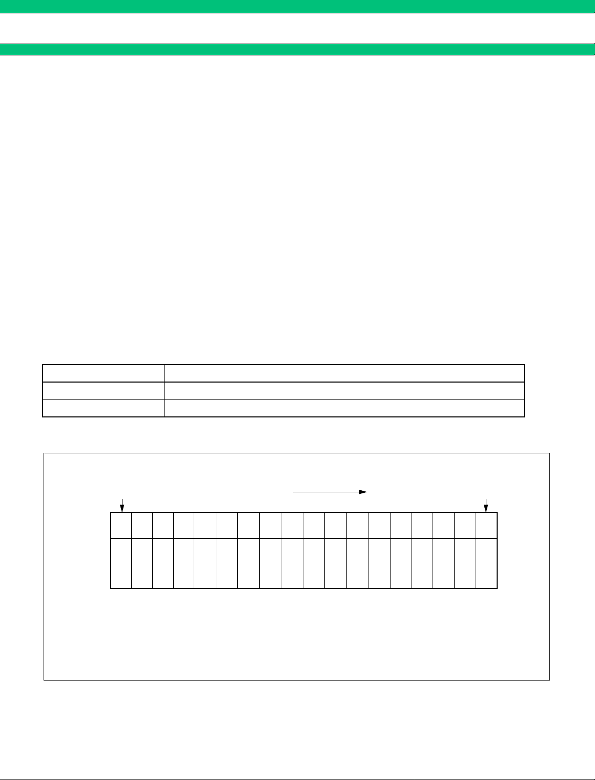
Shift Register Configuration
Programmable Reference Counter
7
R
6
Data
8
R
7
9
10
11
12
R
R
R
R
8
9
10
11
LS
3
2
1
C
N
T
CNT : Control bit [Table. 1]
R1 to R14: Divide ratio setting bit for the programmable reference counter (5 to 16,383) [Table. 2]
SW : Divide ratio setting bit for the prescaler (64/65 or 128/129) [Table. 5]
FC : Phase control bit for the phase comparator [Table. 7]
LDS : LD/fout signal select bit [Table. 6]
R
R
2
1
5
4
R
3
6
R
R
5
4
13
R
12
14
R
13
R
14
SW15FC16LDS
17
MS
18
Note: Start data input with MSB first
7
Page 8
MB15E03
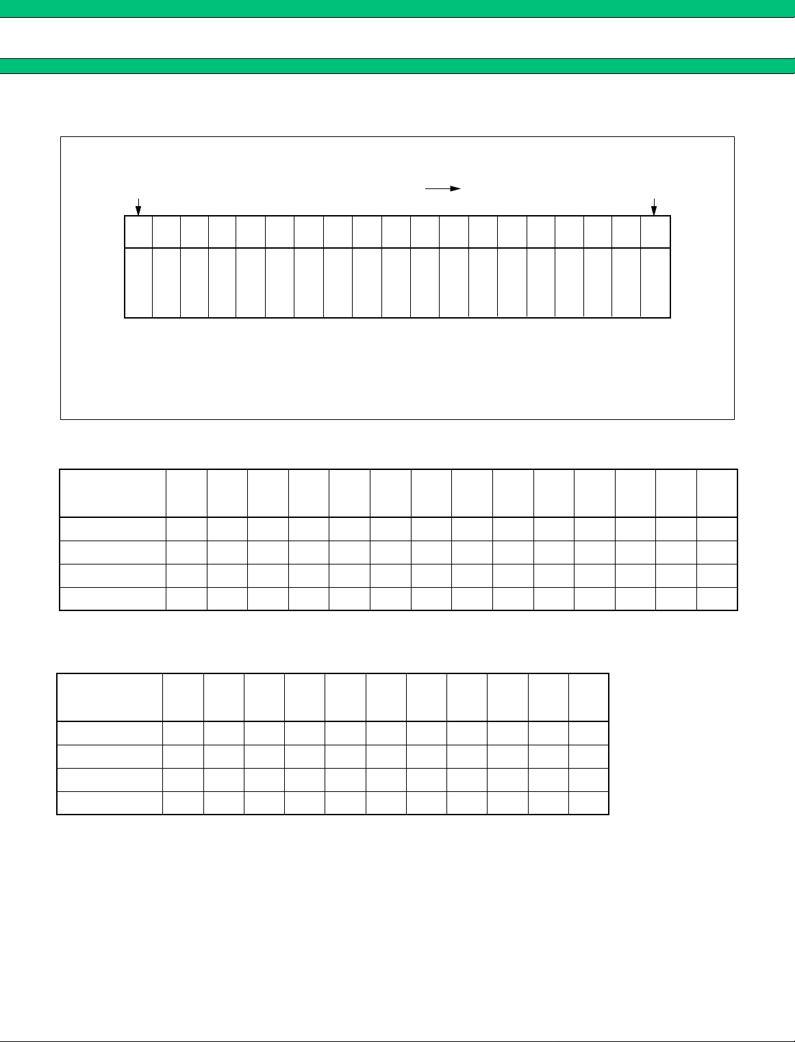
Programmable Reference Counter
8
A
7
Data
9
N
1
10
11
12
13
14
15
16
17
N
N
N
N
N
N
N8N9N10N
2
3
4
5
6
7
LS
1
2 3 45
C
A
A
A
N
1
2
3
T
CNT: Control bit [Table. 1]
N1 to N11: Divide ratio setting bits for the programmable counter (5 to 2,047) [Table. 3]
A1 to A7: Divide ratio setting bits for the swallow counter (0 to 127) [Table. 4]
Note: Start data input with MSB first
A
4
6
A
5
7
A
6
18
MS
19
11
Table2. Binary 14-bit Programmable Reference Counter Data Setting
Divide
ratio
(R)
5 00000000000101
6 00000000000110
⋅ ⋅⋅⋅⋅⋅⋅⋅⋅⋅⋅⋅⋅⋅⋅
16383 11111111111111
R
14R13R12R11R10
R
R
R
9
R
8
7
R
6
R
5
R
4
3
R
R
2
1
Note:• Divide ratio less than 5 is prohibited.
Table.3 Binary 11-bit Programmable Counter Data Setting
Divide
ratio
(N)
5 00000000101
6 00000000110
⋅ ⋅⋅⋅⋅⋅⋅⋅⋅⋅⋅⋅
2047 1 1 111111111
Note:• Divide ratio less than 5 is prohibited.
•
Divide ratio (N) range = 5 to 2,047
8
N
11N10
N
N
N
N
N
9
8
7
6
N
5
4
N
N
3
N
2
1
Page 9
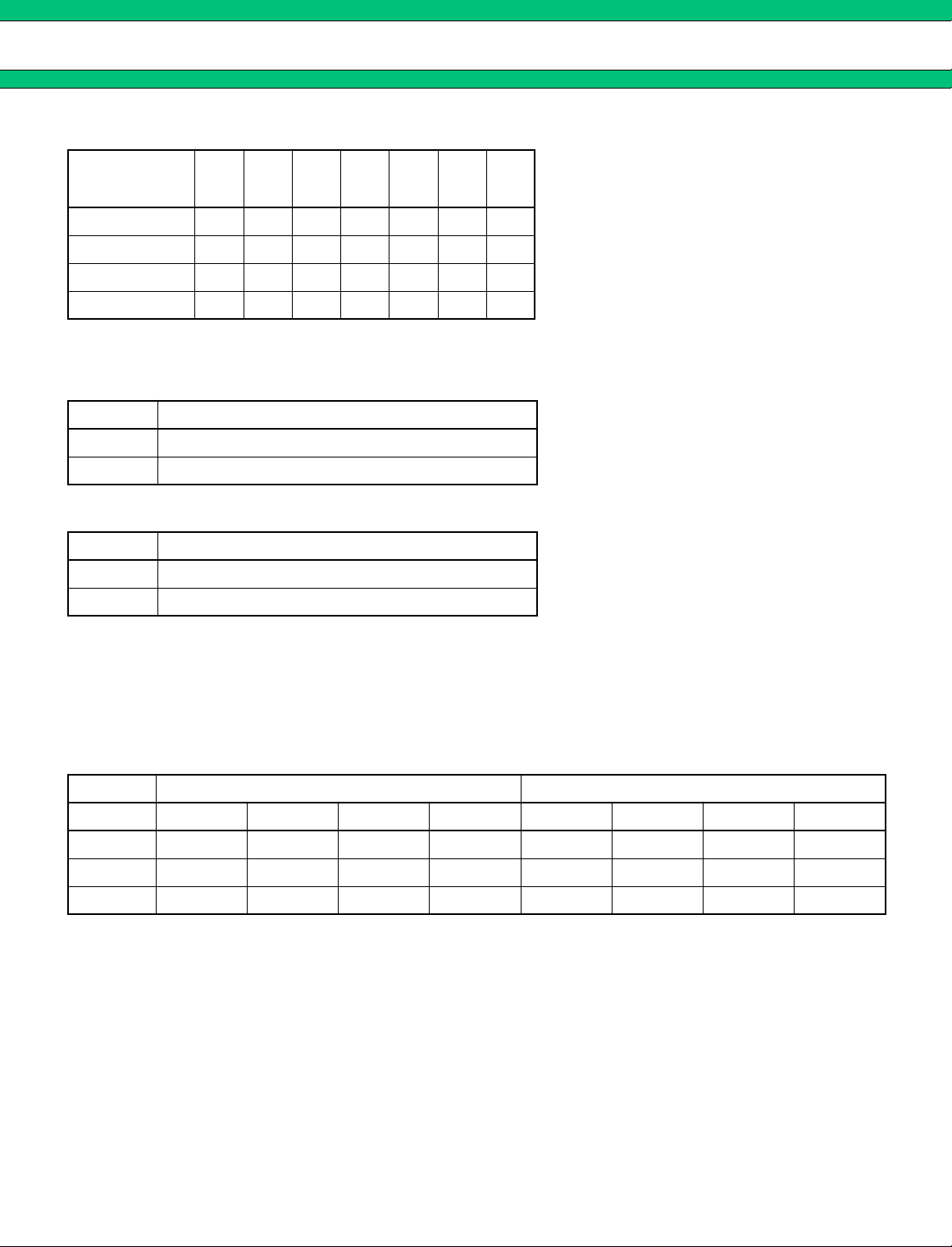
Table.4 Binary 7-bit Swallow Counter Data Setting
Divide
ratio
(A)
0 0000000
1 0000001
⋅ ⋅⋅⋅⋅⋅⋅⋅
127 1 1 1 1 1 1 1
Note: • Divide ratio (A) range = 0 to 127
A
A
A
A
A
A
7
6
5
4
3
A
2
1
Table. 5 Prescaler Data Setting
SW Prescaler Divide ratio
H 64/65
L 128/129
Table. 6 LD/fout Output Select Data Setting
MB15E03
LDS LD/fout output signal
H fout signal
L LD signal
Relation between the FC input and phase characteristics
The FC bit changes the phase characteristics of the phase comparator. Both the internal charge pump output level
(DO) and the phase comparator output (φR, φP) are reversed according to the FC bit. Also, the monitor pin (fOUT)
output is controlled by the FC bit. The relationship between the FC bit and each of DO, φR, and φP is shown below.
Table. 7 FC Bit Data Setting (LDS = ”H”)
FC = High FC = Low
Do φR φP LD/fout Do φR φP LD/fout
fr > fp H L L (fr) L H Z* (fp)
fr < fp L H Z* (fr) H L L (fp)
fr = fp Z* L Z* (fr) Z* L Z* (fp)
* :High impedance
9
Page 10
MB15E03
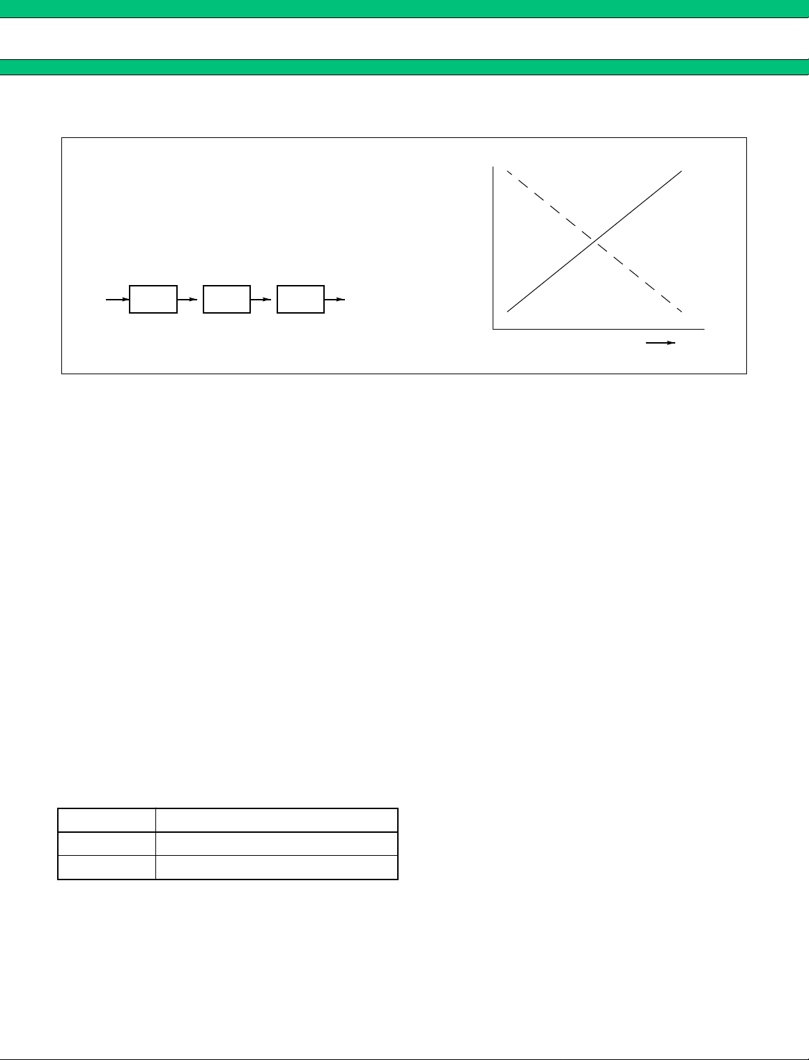
When designing a synthesizer, the FC pin setting depends on the VCO and LPF characteristics.
∗: When the LPF and VCO characteristics are
similar to (1), set FC bit high.
∗: When the VCO characteristics are similar to
(2), set FC bit low.
VCO
Output
Frequency
PLL LPF VC
LPF Input Voltage
(1)
(2)
Power Saving Mode (Intermittent Mode Control Circuit)
Setting a PS pin to Low, the IC enters into power saving mode resultatly current sonsumption can be limited to
10µA (max.). Setting PS pin to High, power saving mode is released so that the IC works normally.
In addition, the intermittent operation control circuit is included which helps smooth start up from the power saving
mode. In general, the power consumption can be sa ved by the intermittent operation that pow ering down or waking
up the synthesizer. Such case, if the PLL is powered up uncontrolled, the resulting phase comparator output signal
is unpredictable due to an undefined phase relation between reference frequency (fr) and comparison frequency
(fp) and may in the worst case take longer time for lock up of the loop.
To prevent this, the intermittent operation control circuit enforces a limited error signal output of the phase detector
during power up, thus keeping the loop locked.
During the power saving mode, the corresponding section except for indispensable circuit for the power saving
function stops working, then current consumption is reduced to 10 µA (max.).
At that time, the Do and LD become the same state as when a loop is locking. That is, the Do becomes high
impedance.
A VCO control voltage is naturally kept at the locking voltage which defined by a LPF”s time constant. As a result
of this, VCO’s frequency is kept at the locking frequency.
Note: •
While the power saving mode is executed, ZC pin should be set at ”H” or open. If ZC is set at ”L”
during power saving mode, approximately 10 µA current flows.
•
PS pin must be set ”L” at Power-ON.
•
The power saving mode can be released (PS : L
•
During the power saving mode, it is possible to input the serial data.
Table.8 PS Pin Setting
PS pin Status
H Normal mode
L Power saving mode
10
→
H) 1µs later after power supply remains stable.
Page 11
V
CC
Clock
Data
LE
PS
MB15E03
ON
i1j i2j i3j
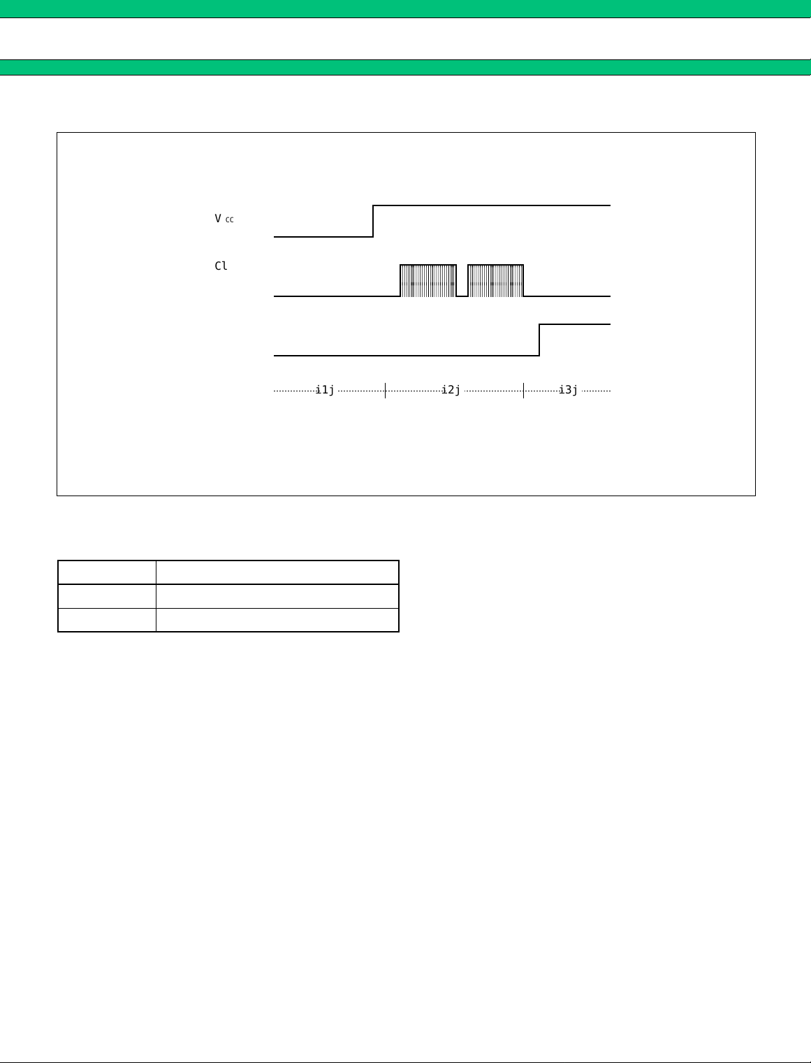
(1) PS = L (power saving mode) at Power-ON.
(2) Set serial data after power supply remains stable.
(3) Release saving mode (PS: LfiH) after setting serial data.
Table.9 ZC Pin Setting
ZC pin Do output
H Normal output
L High impedance
11
Page 12
MB15E03
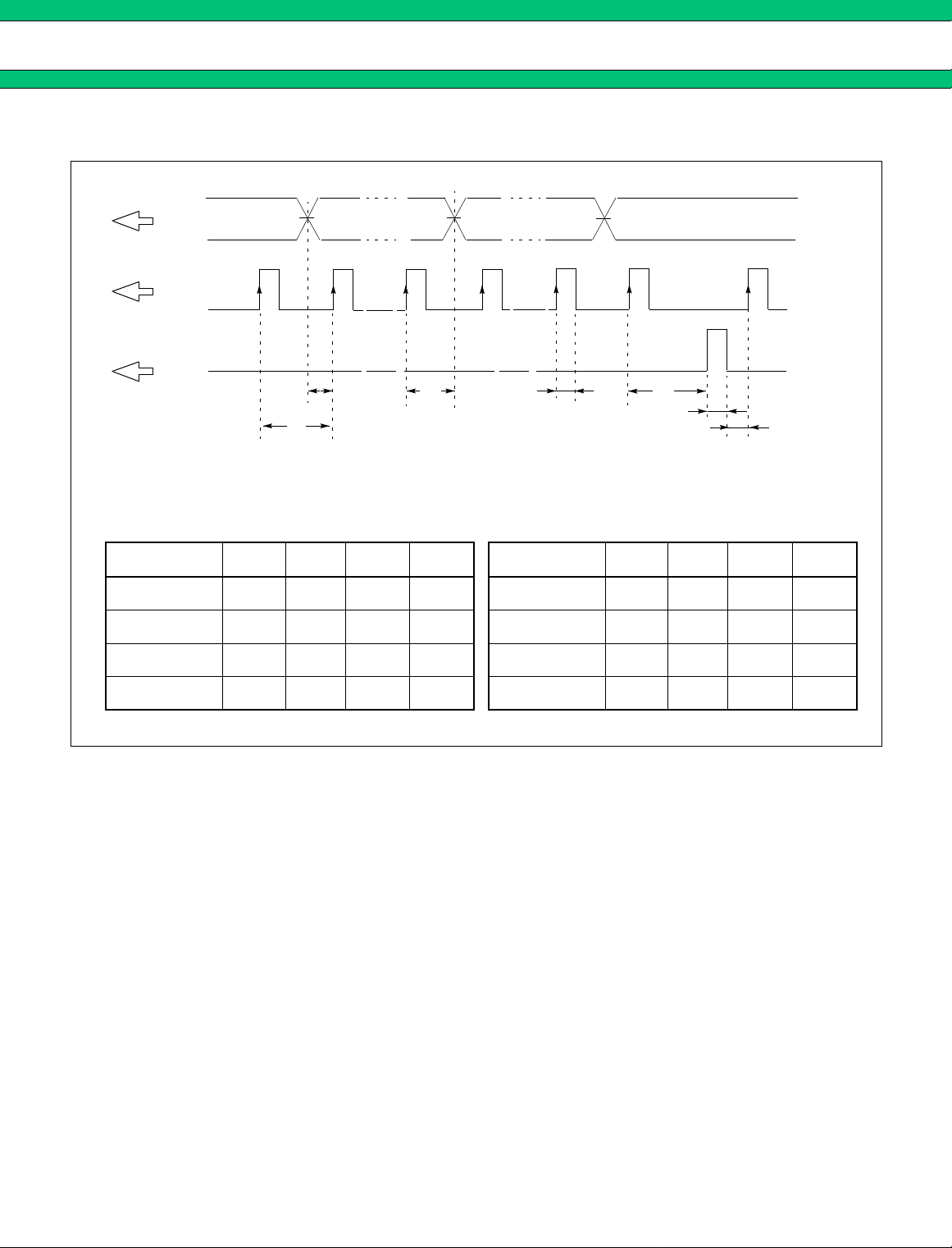
■ SERIAL DATA INPUT TIMING
Data
Clock
LE
On rising edge of the clock, one bit of the data is transferred into the shift register.
Parameter
t1
t2
t3
t4
MSB LSB
t2
t3
t4
t1
20
20
30
30
UnitMax.Typ.Min.
–
–
–
–
–
–
–
–
ns
ns
ns
ns
Parameter
t5
t6
t7
100
20
100
t5
t6t7
UnitMax.Typ.Min.
–
–
–
–
–
–
ns
ns
ns
12
Page 13
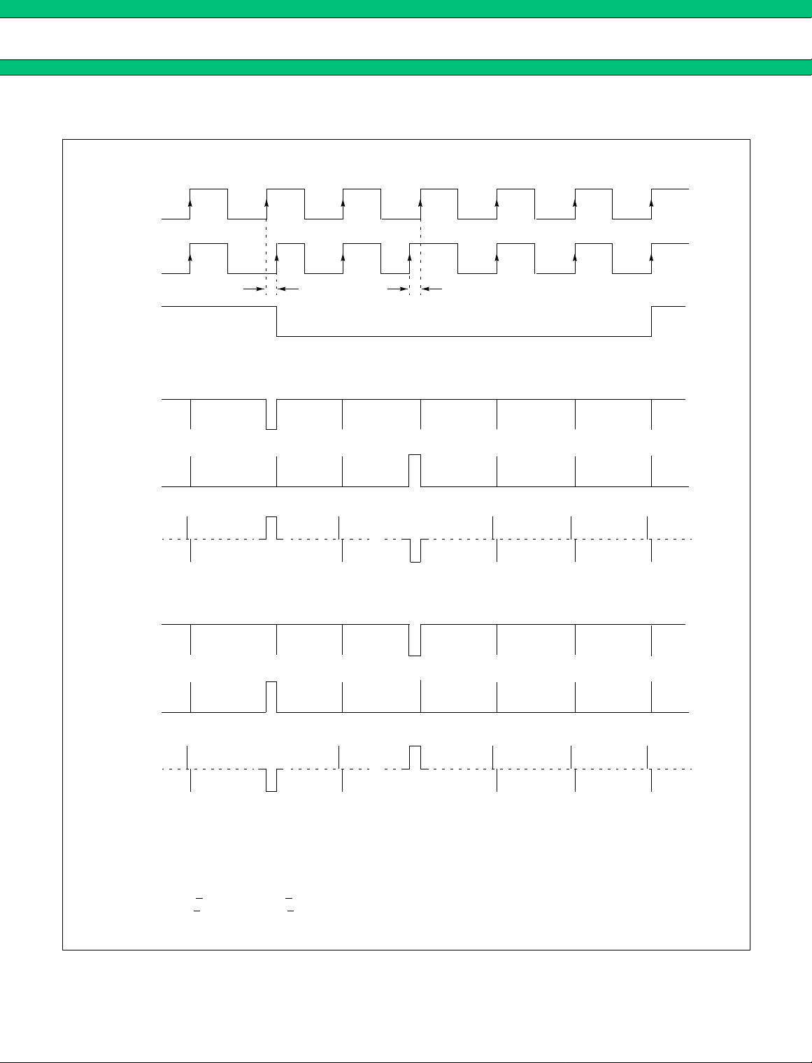
■ PHASE COMPARATOR OUTPUT WAVEFORM
fr
fp
tWU tWL
LD
[ FC = ”H” ]
φP
MB15E03
φR
H
Do
[ FC = ”L” ]
φP
φR
Do
L
Notes: 1. Phase error detection range: –2π to +2π
2. Pulses on Do output signal during locked state are output to prevent dead zone.
3. LD output becomes low when phase is t
or less and continues to be so for three cysles or more.
4. t
WU and tWL depend on OSCin input frequency.
tWU > 8/fosc (e. g. tWU > 625ns, foscin = 12.8 MHz)
5. LD becomes high during the power saving mode (PS = ”L”.)
tWL < 16/fosc (e. g. tWL < 1250ns, foscin = 12.8 MHz)
Z
L
H
Z
WU or more. LD output becomes high when phase error is tWL
13
Page 14
MB15E03
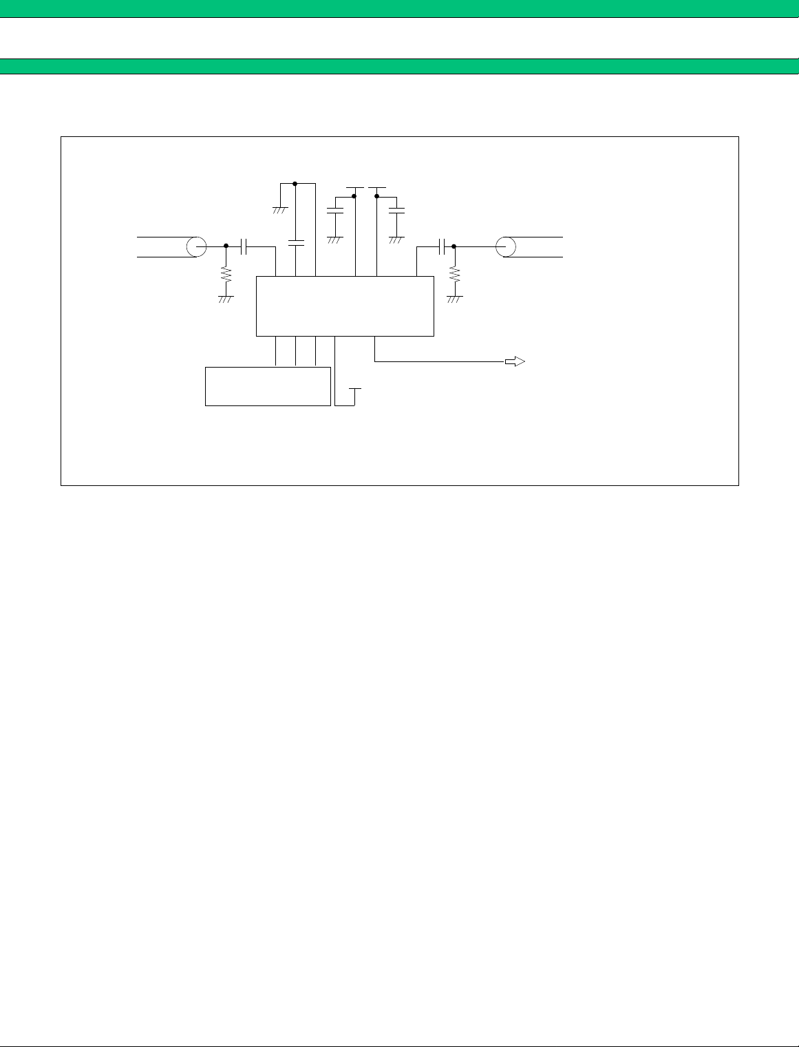
■ TEST CIRCUIT (FOR MEASURING INPUT SENSITIVITY FIN/OSCIN)
VCC VP
0.1µF
1000pF
P • G P • G
1000pF
50 Ω
87654321
9 10111213141516
Controller
(setting divide ratio)
0.1µF
Vcc
1000pF
50 Ω
Oscilloscope
Note: SSOP-16 pin
14
Page 15
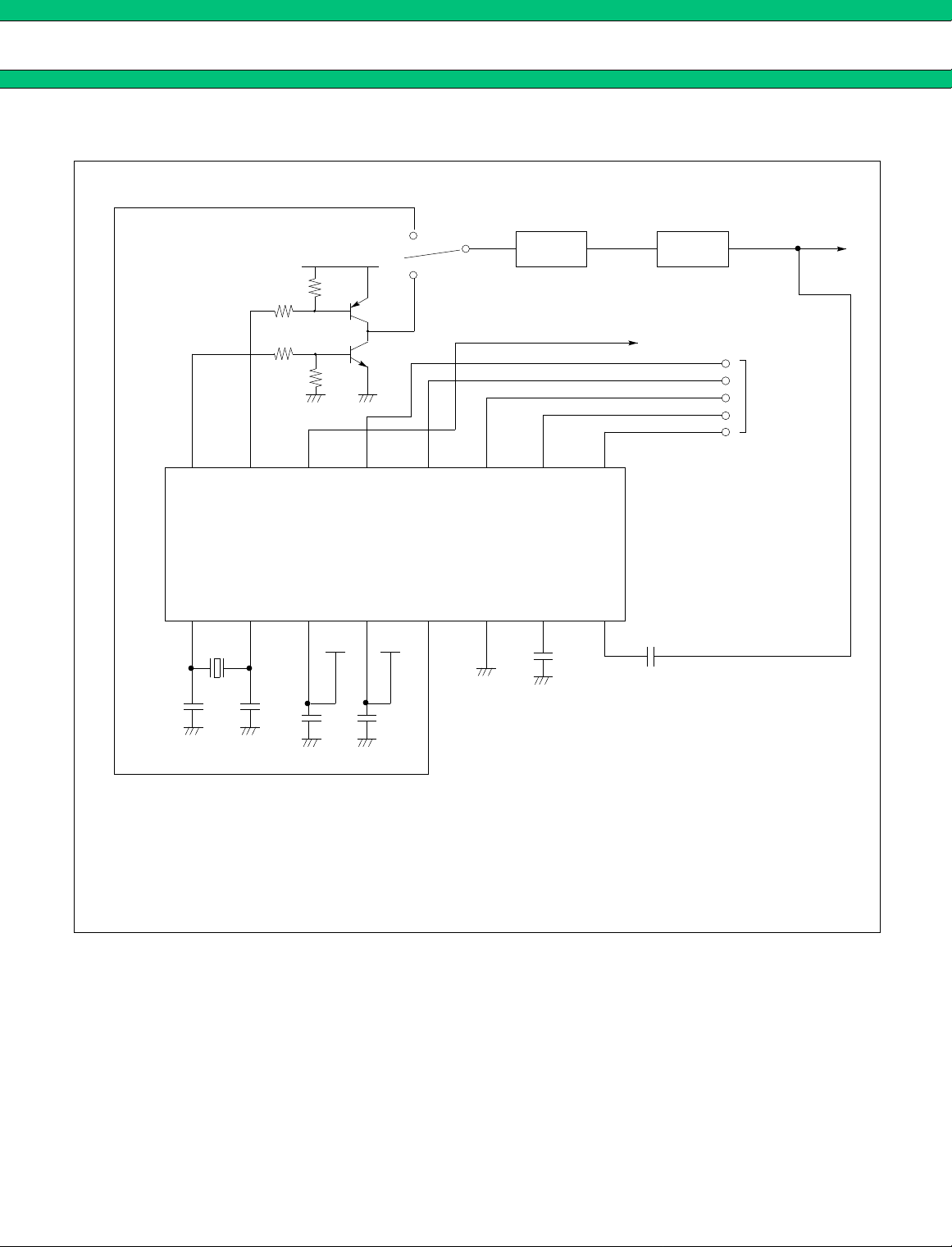
■ APPLICATION EXAMPLE
MB15E03
10kΩ
12kΩ
12kΩ
φR φP LD/FOUT ZC PS LE Data Clock
16 15 14 13 12 11 10 9
MB15E03
12345678
OSCIN OSCOUT VP VCC DO GND XfIN fIN
X’ tal
1
C
C2
10kΩ
0.1µF
0.1µF
LPF VCO
To a lock detect.
1000pF
1000pF
Output
From
a controller
C1, C2 : Depend on the crystal parameters
Note: SSOP-16 pin
15
Page 16
MB15E03
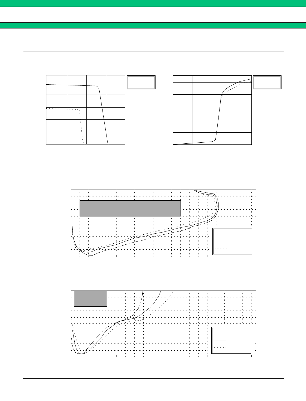
■ TYPICAL CHARACTERISTICS
Do Output Current
[Ta = +25°C]
[V
CC = 3 V, Vp =3 V, 5 V]
5.0
4.0
Vp = 3 V
Vp = 5 V
5.0
4.0
[Ta = +25°C]
[V
CC = 3 V, Vp =3 V, 5 V]
Vp = 3 V
Vp = 5 V
3.0
2.0
VOH (V)
1.0
0
0
–5
–10 –15 –20
I
OH (mA)
fin Input Sensitivity
[Ta = +25°C]
+10
0
–10
–20
Vfin (dBm)
–30
–40
0
OSCin Input Characteristics
[Ta = +25°C]
+10
SPEC
0
VOL (V)
SPEC
500 1000
fin (MHz)
3.0
2.0
1.0
0
0
5
10 15 20
OL (mA)
I
Main. counter div. ratio = 4104
Swallow="ON"
V
CC = Vp
Xfin = 1000 pF pull down
VCC=2.7 V
VCC=3.0 V
VCC=3.6 V
1500
2000
Ref. counter div. ratio = 2048
CC = Vp
V
fin = 1.2 GHz (–10 dBm)
16
–10
–20
Vfosc (dBm)
–30
–40
VCC=2.7 V
VCC=3.0 V
VCC=3.6 V
0
50 100
150
200
fosc (MHz)
(Continued)
Page 17
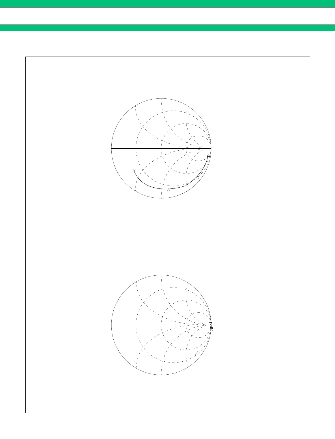
(Continued)
fin Input Impedance
MB15E03
fin
START 100.000 000 MHZ STOP 1 200.000 000 MHZ
OSCin Input Impedance
4: 9.0039 Ω –19.444 Ω
1 200.000 000 MHz
6.821 pF
1: 232.63 Ω
–556.66 Ω
100 MHz
2: 22.031 Ω
–150.96 Ω
400 MHz
3: 9.8965 Ω
1
4
2
3
–59.148 Ω
800 MHz
2: 694.75 Ω –5.339 kΩ
2.981 pF
10.000 000 MHz
1: 4.094 kΩ
–15.619 kΩ
3 MHz
3: 437.5 Ω
–2.7839 kΩ
20 MHz
–1.508 kΩ
OSCin
2
4: 163.81 Ω
3
1
4
40 MHz
START 3.000 000 MHZ STOP 40.000 000 MHZ
17
Page 18
MB15E03
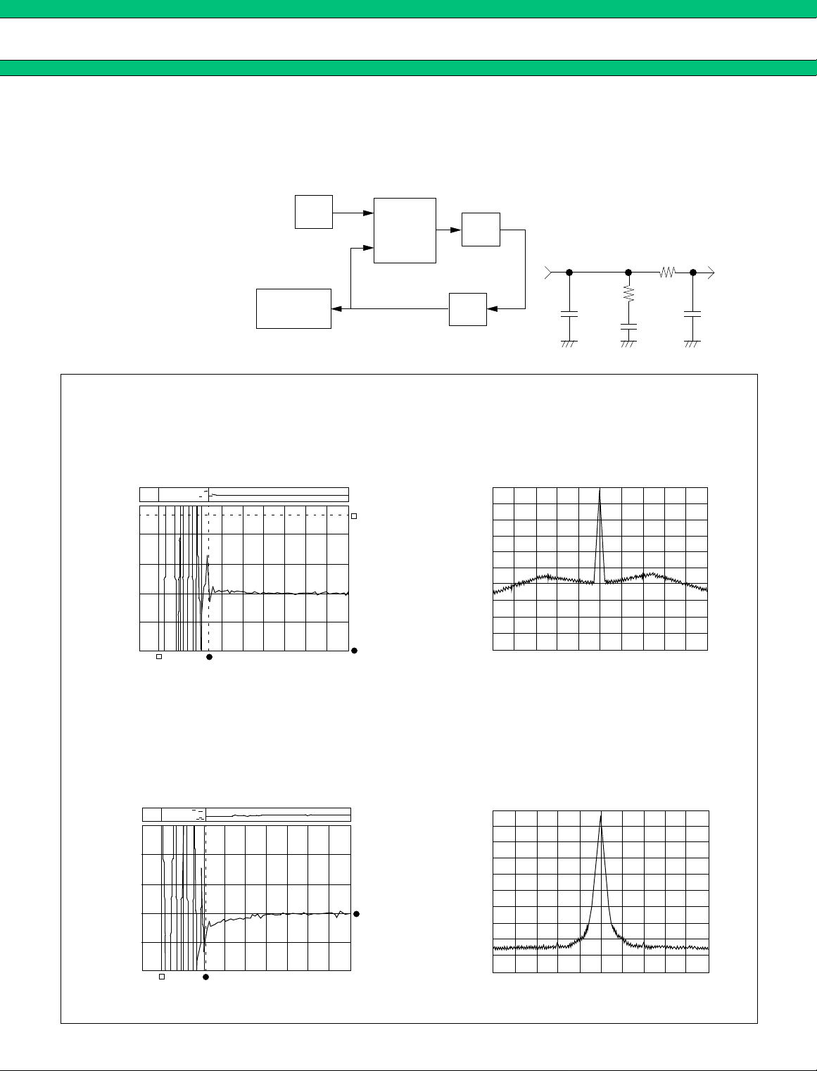
■ REFERENCE INFORMATION
Typical plots measured with the
test circuit are shown below.
Each plot shows lock up time,
phase noise and reference
leakage.
S.G
OSCin
fin
Spectrum
Analyzer
PLL Lock Up Time = 440 µs
(1005.000 MHz → 1031.000 MHz, within ± 1kHz)
∆ MKr x : 439.89783 µs
y : 25.94979 MHz
30.00300
MHz
Do
Test Circuit
LPF
VCO
REF
10dB/
• fvco = 1018 MHz
• Kv = 20 MHz/v
• fr = 200 kHz
• fosc = 13 MHz
• LPF:
15 kΩ
2.2 kΩ
2000 pF
20000 pF
PLL Phase Noise
@ within loop band = 76.2 dBc/Hz
–10.0 dBm
ATT 10 dB MKR ∆12.40 kHz
–51.2 dB
330 pF
1.000
kHz/div
29.99800
MHz
10.2702 µs 1.9902702 ms
PLL Lock Up Time = 400 µs
(1031.000 MHz → 1005.000 MHz, within ± 1kHz)
∆ MKr x : 400.00973 µs
y : –25.094747 MHz
30.00300
MHz
1.00
kHz/div
29.99800
MHz
10.1432 µs 1.9901432 ms
RBW
300 Hz
VBW
300 Hz
REF
10dB/
RBW
10 kHz
VBW
10 kHz
SPAN 50.0 kHz CENTER 1.0180000 GHz
PLL Reference Leakage
@ 200 kHz offset = 79.0 dBc
–10.0 dBm
SPAN 1.00 MHz CENTER 1.01800 GHz
ATT 10 dB MKR ∆ 204 kHz
–79.0 dB
18
Page 19

■ ORDERING INFORMATION
Part number Package Remarks
MB15E03 PFV1
MB15E03 PV
MB15E03
16 pin, Plastic SSOP
(FPT-16P-M05)
16 pin, Plastic BCC
(LCC-16P-M02)
19
Page 20
MB15E03
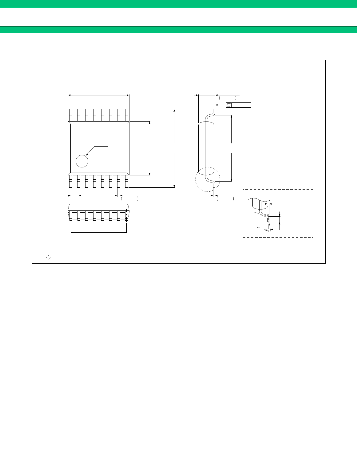
■ PACKAGE DIMENSIONS
16 pins, Plastic SSOP
(FPT-16P-M05)
*
5.00±0.10(.197±.004)
0.65±0.12
(.0256±.0047)
4.55(.179)REF
INDEX
* : These dimensions do not include resin protrusion.
*
4.40±0.10 5.40(.213)
(.173±.004) (.252±.008) NOM
+0.10
0.22
–0.05
+.004
.009
–.002
6.40±0.20
"A"
0.15
.006
1.25
.049
+0.20
–0.10
+.008
–.004
0.10(.004)
+0.05
–0.02
+.002
–.001
Details of "A" part
0 10°
0.10±0.10(.004±.004)
(STAND OFF)
0.50±0.20
(.020±.008)
C
1994 FUJITSU LIMITED F16013S-2C-4
Dimensions in mm (inches).
(Continued)
20
Page 21
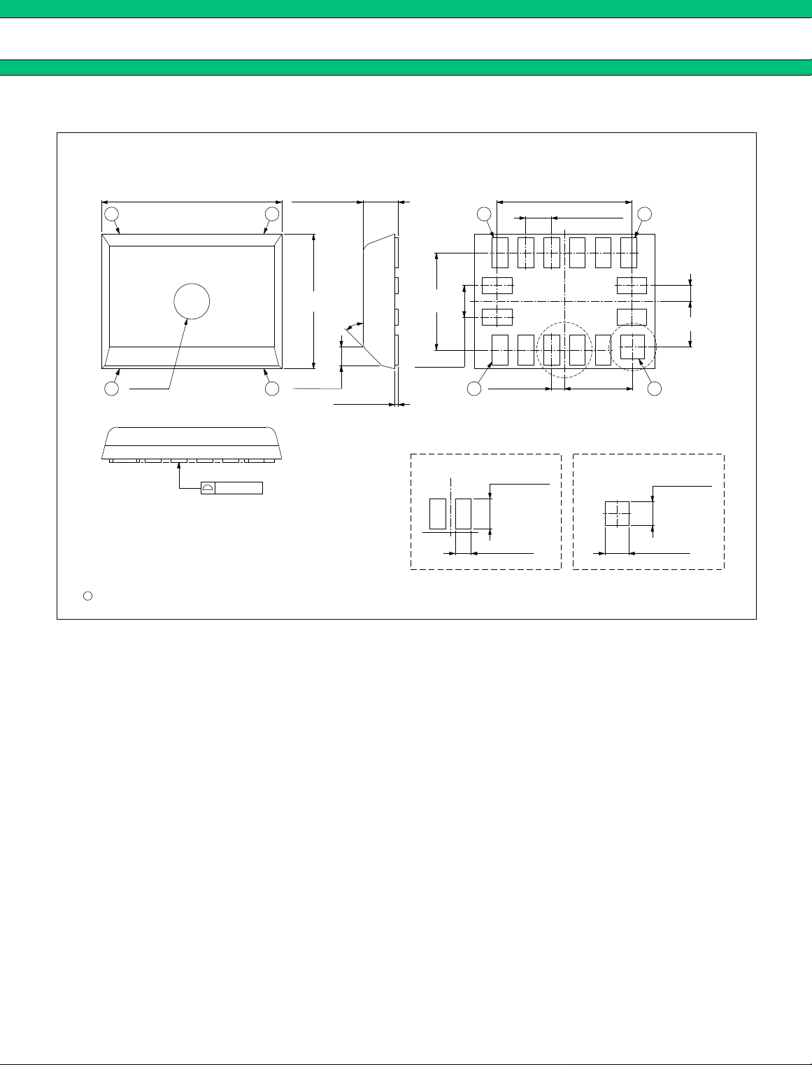
16-pin, Plastic BCC
(LCC-16P-M02)
4.55±0.10
14
(.179±.004)
0.80(.032)MAX
(Mounting height)
9
MB15E03
3.40(.134)TYP
9
0.65(.026)TYP
14
0.40±0.10
(.016±.004)
3.40±0.10
(.1339±.0039)
E-MARK
1
0.05(.002)
C
1996 FUJITSU LIMITED C16013S-1C-1
6
0.40(.016)
45˚
0.085±0.04
(.003±.002)
(STAND OFF)
2.45(.096)
TYP
0.80(.032)
TYP
6
Details of "A" part
0.325±0.10
(.013±.004)
0.75±0.10
(.030±.004)
0.40±0.10
(.016±.004)
"A"
"B"
1.725(.068)
TYP
Details of "B" part
1.15(.045)TYP
1
0.60±0.10
(.024±.004)
0.60±0.10
(.024±.004)
Dimensions in mm (inches)
21
Page 22

MB15E03
FUJITSU LIMITED
For further information please contact:
Japan
FUJITSU LIMITED
Corporate Global Business Support Division
Electronic Devices
KAWASAKI PLANT, 4-1-1, Kamikodanaka
Nakahara-ku, Kawasaki-shi
Kanagawa 211-88, Japan
Tel: (044) 754-3763
Fax: (044) 754-3329
All Rights Reserved.
The contents of this document are subject to change without
notice. Customers are advised to consult with FUJITSU sales
representatives before ordering.
North and South America
FUJITSU MICROELECTRONICS, INC.
Semiconductor Division
3545 North First Street
San Jose, CA 95134-1804, U.S.A.
Tel: (408) 922-9000
Fax: (408) 432-9044/9045
Europe
FUJITSU MIKROELEKTRONIK GmbH
Am Siebenstein 6-10
63303 Dreieich-Buchschlag
Germany
Tel: (06103) 690-0
Fax: (06103) 690-122
Asia Pacific
FUJITSU MICROELECTRONICS ASIA PTE. LIMITED
#05-08, 151 Lorong Chuan
New Tech Park
Singapore 556741
Tel: (65) 281 0770
Fax: (65) 281 0220
The information and circuit diagrams in this document presented
as examples of semiconductor device applications, and are not
intended to be incorporated in devices for actual use. Also,
FUJITSU is unable to assume responsibility for infringement of
any patent rights or other rights of third parties arising from the
use of this information or circuit diagrams.
FUJITSU semiconductor devices are intended for use in
standard applications (computers, office automation and other
office equipment, industrial, communications, and measurement
equipment, personal or household devices, etc.).
CAUTION:
Customers considering the use of our products in special
applications where failure or abnormal operation may directly
affect human lives or cause physical injury or property damage,
or where extremely high levels of reliability are demanded (such
as aerospace systems, atomic energy controls, sea floor
repeaters, vehicle operating controls, medical devices for life
support, etc.) are requested to consult with FUJITSU sales
representatives before such use. The company will not be
responsible for damages arising from such use without prior
approval.
Any semiconductor devices have inherently a certain rate of
failure. You must protect against injury, damage or loss from
such failures by incorporating safety design measures into your
facility and equipment such as redundancy, fire protection, and
prevention of over-current levels and other abnormal operating
conditions.
F9704
FUJITSU LIMITED Printed in Japan
22
If any products described in this document represent goods or
technologies subject to certain restrictions on export under the
Foreign Exchange and Foreign Trade Control Law of Japan, the
prior authorization by Japanese government should be required
for export of those products from Japan.
 Loading...