

Page 1
September 1995
Edition 6.0a
DA TA SHEET
MB1501/MB1501H/MB1501L
SERIAL INPUT PLL FREQUENCY SYNTHESIZER
SERIAL INPUT PLL FREQUENCY SYNTHESIZER
WITH 1.1GHz PRESCALER
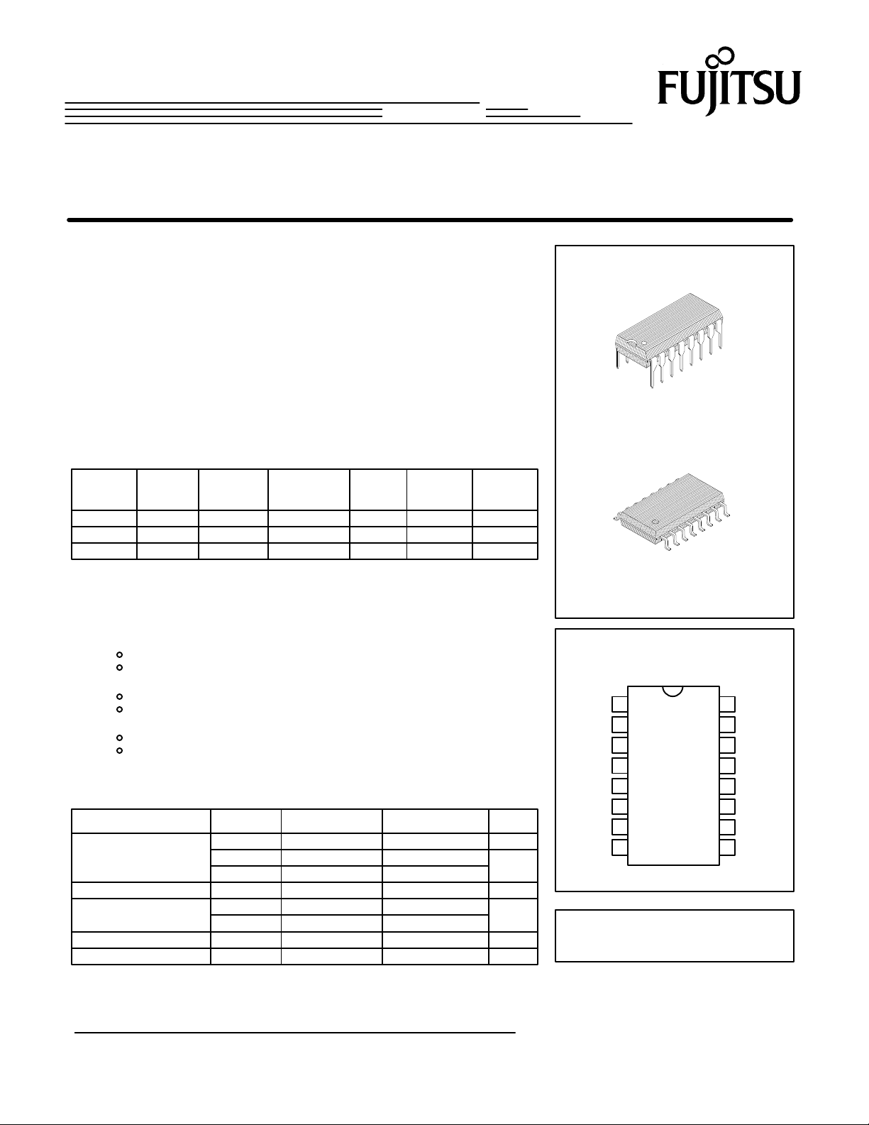
The Fujitsu MB1501/MB1501H/MB1501L, utilizing BI-CMOS technology, is a
single chip serial input PLL frequency synthesizer with pulse-swallow function.
The MB1501 series contain a 1.1GHz two modulus prescaler that can select either
64/65 or 128/129 divide ratio; control signal generator; 16-bit shift register; 15-bit
latch; programmable reference divider (binary 14-bit programmable reference
counter); 1-bit switch counter; phase comparator with phase inverse function;
charge pump; crystal oscillator; 19-bit shift register; 18-bit latch; programmable
divider (binary 7-bit swallow counter and binary 1 1-bit programmable counter).
The MB1501 operates on a low supply voltage (3V typ) and consumes low power
(45mW at 1.1GHz).
MB1501 Product Line
High-level
Output
Current
MB1501
D
V
P
Voltage
V
OOP
Voltage
Lock up
time
O
Output
Width
8V max 8.5V max Middle speed Middle Middle Middle
MB1501H 10V max 10.0V max High speed Low High Low
MB1501L 8V max 8.5V max Low speed High Low High
Low-level
Output
Current
PLASTIC PACKAGE
DIP-16P-M04
• High operating frequency: f
IN MAX
=1.1GHz (P
IN MIN
=0.20V
P-P
)
• On-chip prescaler
• Low power supply voltage: 2.7V to 5.5V (3.0V typ)
• Low power supply consumption: 45mW (3.0V, 1.1GHz operation)
• Serial input 18-bit programmable divider consisting of:
Binary 7-bit swallow counter (Divide ratio: 0 to 127)
Binary 1 1-bit programmable counter (Divide ratio: 16 to 2047)
• Serial input 15-bit programmable reference divider consisting of:
Binary 14-bit programmable reference counter (Divide ratio: 8 to 16383)
1-bit switch counter (SW) Sets divide ratio of prescaler
• 2types of phase detector output
On-chip charge pump (Bipolar type)
Output for external charge pump
• Wide operating temperature: T
=–40°C to +85°C
A
ABSOLUTE MAXIMUM RA TINGS (see NOTE)
Rating
Power Supply Voltage
Output Voltage
Open-drain Output
Output Current
Storage Temperature
NOTE: Permanent device damage may occur if the above Absolute Maximum Ratings
are exceeded. Functional operation should be restricted to the conditions as
detailed in the operational sections of this data sheet. Exposure to absolute
maximum rating conditions for extended periods may affect device reliability.
Symbol Value
V
CC
V
PH
VP,V
PL
V
OUT
V
OOPH
V
OOP,VOOPL
I
OUT
T
STG
Condition
–0.5 to +7.0
MB1501H
MB1501/1501L V
V
CC
CC
–0.5 to V
MB1501H
–0.5 to 1 1.0
MB1501/1501L –0.5 to 9.0
–55 to +125
to 12.0
to 10.0
+0.5
CC
±10
Unit
V
V
V
V
mA
°C
PLASTIC PACKAGE
FPT-16P-M06
PIN ASSIGNMENT
1
IN
OSC
This device contains circuitry to protect the inputs against
damage due to high static voltages or electric fields. However, it is advised that normal precautions be taken to avoid
application of any voltage higher than maximum rated voltages to this high impedance circuit.
2
OUT
3
V
P
4
V
CC
D
GND
LD
( TOP VIEW )
5
O
6
7
89
f
in
16OSC
15
14
13
12
11
10
ØR
ØP
f
P
f
r
FC
LE
Data
Clock
Copyright 1994 by FUJITSU LIMITED and FUJITSU MICROELECTRONICS, INC.
1
Page 2
MB1501
MB1501H
MB1501L
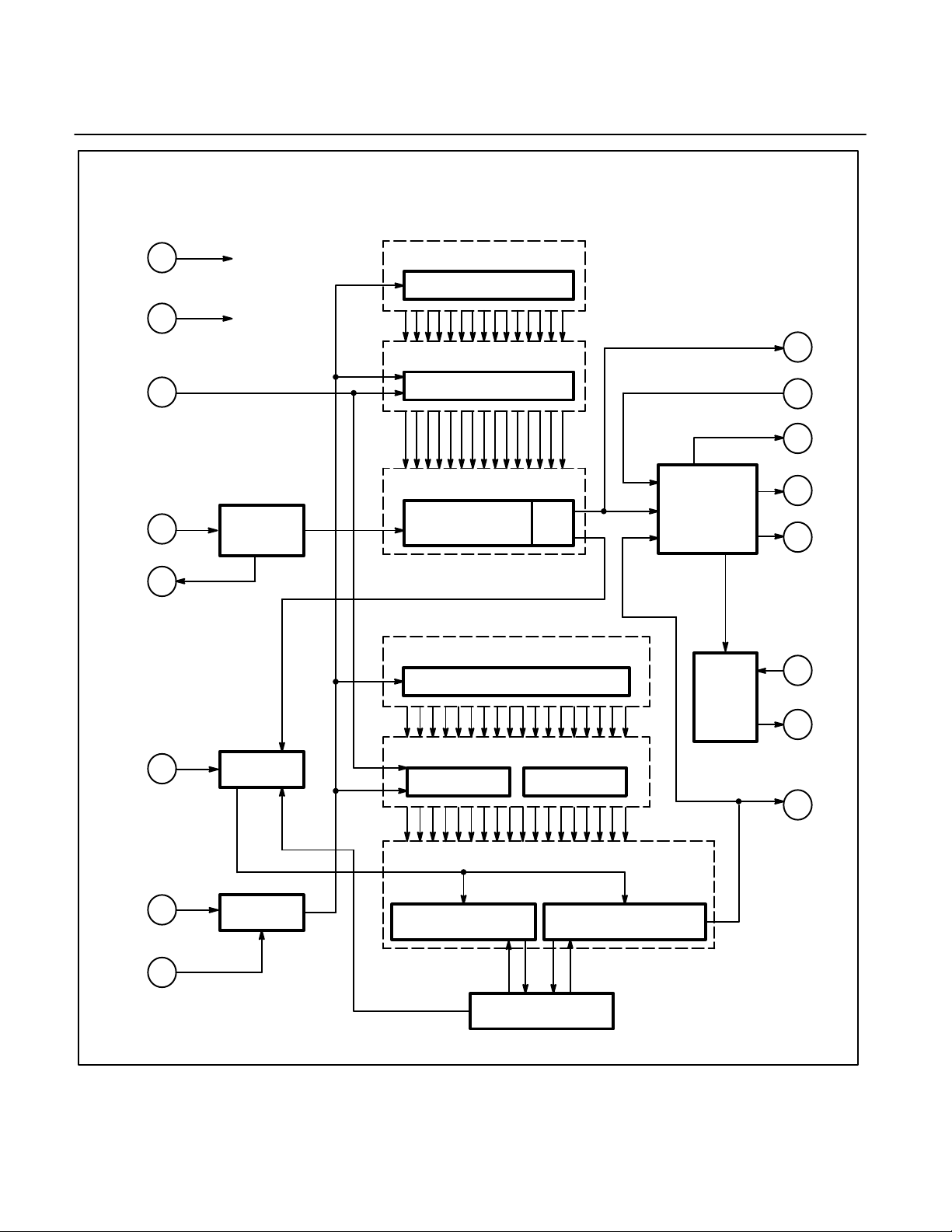
MB1501/MB1501H/MB1501L BLOCK DIAGRAM
OSC
OSC
V
CC
GND
OUT
4
16-Bit Shift Register
16-Bit Shift Register
6
f
13
12
16
15
r
FC
LD
7
R
P
15-Bit Latch
11LE
15-Bit Latch
Programmable
Reference Divider
1
IN
Oscillator
Circuit
Crystal
Binary 14-Bit
Reference Counter
1-bit
SW
Phase
Comparator
2
19-Bit Shift Register
V
3
19-Bit Shift Register
Charge
P
Pump
D
5
O
8f
in
Prescaler
Circuit
7-Bit Latch 1 1-Bit Latch
18-Bit Latch
14
f
P
Programmable Divider
10Data
Control
1-Bit Latch
Binary 7-Bit
Swallow Counter
Binary 11-Bit
Programmable Counter
9Clock
Control Circuit
2
Page 3
PIN DESCRIPTIONS
MB1501
MB1501H
MB1501L
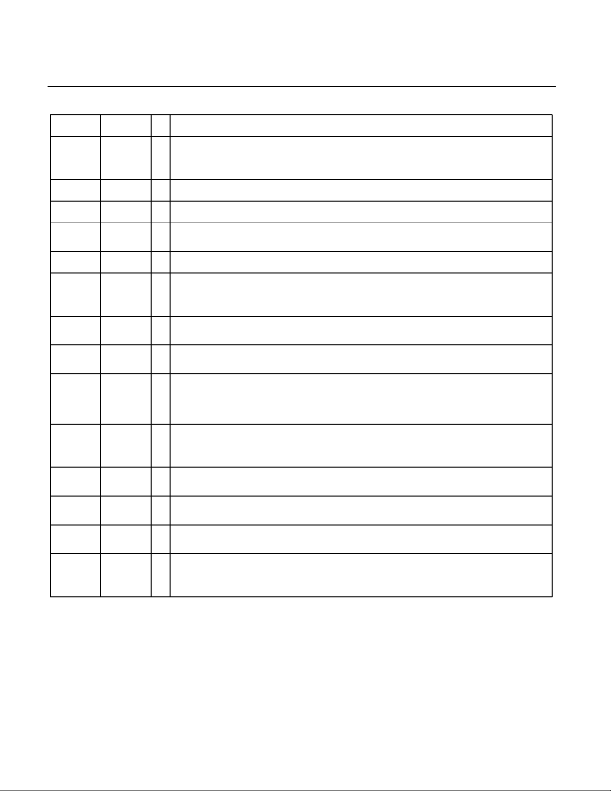
Pin No. Pin Name Descriptions
1
2
3
4
5
OSC
OSC
V
V
D
6 GND Ground.
P
CC
O
IN
OUT
I/O
Oscillator input.
I
O
Oscillator output.
A crystal is placed between OSC
Power supply input for charge pump.
—
Power supply voltage input.
—
Charge pump output.
O
Phase characteristic can be inversed depending upon FC input.
and OSC
IN
OUT
.
—
Phase comparator output.
7
LD
O
This pin outputs high when the phase is locked. While the phase difference of f
the output level goes low.
Prescaler input.
8
f
in
Clock9
I
The connection with an external VCO should be an AC connection.
Clock input for 19-bit shift register and 16-bit shift register.
I
Each rising edge of the clock shifts one bit of data into the shift registers.
Serial data of binary code input.
The last bit of the data is a control bit. The last data bit specifies which latch is activated.
10 Data
I
When the last bit is high level and LE is high-level, data is transferred to 15-bit latch.
When the last bit is low level and LE is high level, data is transferred to 18-bit latch.
and fp exists,
r
11 LE
12
FC
13
14
15
16
f
P
R
Load enable input (with internal pull up resistor).
I
When LE is high level (or open), data stored in the shift register is transferred to latch depending on the control data.
Phase selecting input of phase comparator (with internal pull up resistor). When FC is low
O
level, charge pump and phase detector characteristics can be inversed.
f
r
P
Monitor pin of phase comparator input.
O
It is the same as programmable reference divider output.
Monitor pin of phase comparator input.
O
It is the same as programmable divider output.
O
Outputs for external charge pump.
O
Phase characteristics can be inversed depending on FC input.
P pin is an N-channel open-drain output.
3
Page 4
MB1501
MB1501H
MB1501L
FUNCTIONAL DESCRIPTIONS
SERIAL DATA INPUT
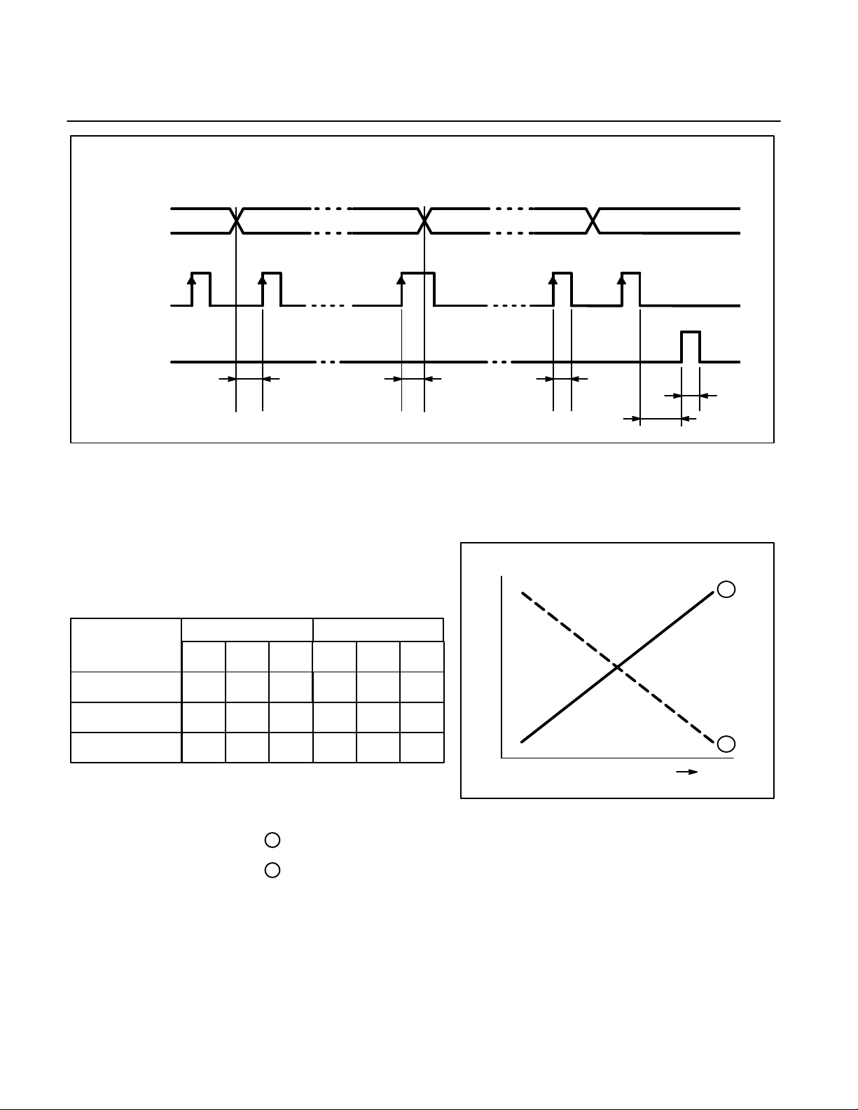
Serial data input is input using Data pin, Clock pin and LE pin, The 15-bit programmable reference divider and 18-bit programmable
divider are controlled respectively.
On rising edge of the clock shifts one bit of the data into the internal shift registers.
When load enable (LE) is high level (or open), data stored in shift resisters is transferred to 15-bit latch or 18-bit latch depending upon
the control bit level.
Control data “H” ; Data is transferred into 15-bit latch.
Control data “L” ; Data is transferred into 18-bit latch.
PROGRAMMABLE REFERENCE DIVIDER
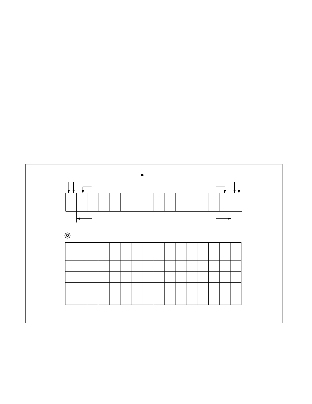
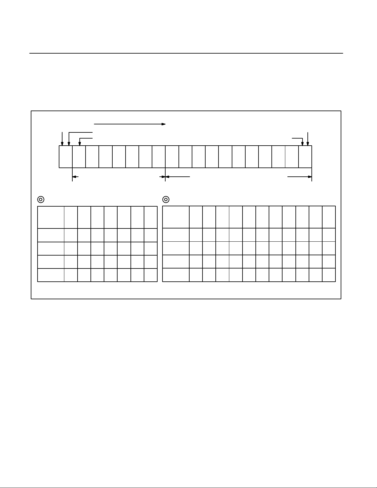
Programmable reference divider consists of 16-bit shift register, 15-bit latch and 14-bit reference counter . Serial 16-bit data format is
shown below.
Data input
Control bit
LSB
SSS
S
1234
Divide ratio of programmable reference counter setting bits
14-BIT PROGRAMMABLE REFERENCE COUNTER DIVIDE RATIO
Divide
ratio
R
8
9
SSS
S
14 13 12 11S10S9S8S7S6S5S43
0
0
S
5
000000001000
Divide ratio of prescaler setting bit
S
S
S
S
S10S
6
7
8
9
11 12
MSB
SS13S
14
SS
2
• ••••••••••••••
16383 1 1 1 1 1 111111111
Divide ratio less than 8 is prohibited.
Divide ratio R: 8 to 16383
First data inputLast data input
SWC
S
1
10010000000000
SW: Divide ratio of prescaler setting bit.
S
C: Control bit (Control bit is set to high.)
SW=“H” : 64
SW=“L” : 128
to S14: Divide ratio of programmable reference counter setting bits (8 to 16383)
1
4
Page 5
MB1501
MB1501H
MB1501L
FUNCTIONAL DESCRIPTIONS
PROGRAMMABLE DIVIDER
Programmable divider consists of 19-bit shift register, 18-bit latch, 7-bit swallow counter and 11-bit programmable counter.
Serial 19-bit data format is shown below.
Last data input
C
7-BIT SWALLOW COUNTER DIVIDE RATIO
Divide
ratio
A
0
1
S7S6S5S
0000000
Control bit
LSB
SSS
S
1234
Divide ratio of swallow counter
setting bits
43
S
5
SS
• •••••••
127 1111111
Divide ratio A : 0 to 127
2
S
6
S
1
1000000
Data input
S
S
S
S10S
7
8
9
Divide ratio of programmable counter
11-BIT PROGRAMMABLE COUNTER DIVIDE RATIO
Divide
ratio
N
16
17
SSS
18 17 16 15S14S13S12S11S10S9S8
00000010000
SS13S14S
11 12
setting bits
S
15S16S17S18
First data input
MSB
• •••••••••••
2047 1
Divide ratio less than 16 is prohibited.
Divide ratio N : 16 to 2047
1111111 111
10001000000
S8 to S18:Divide ratio of programmable counter setting bits (16 to 2047)
to S7: Divide ratio of swallow counter setting bits (0 to 127)
S
1
C: Control bit (Control bit is set to low.)
Dara is input from MSB data.
5
Page 6
MB1501
MB1501H
MB1501L
SERIAL DATA INPUT TIMING
Data
S18=MSB
*(SW) (S14)
S17
S10
S9
(S8) (S7)
S1=LSB
(S1)
Clock
LE
t
1
– t
≥ 1µs
t
1
5
t
2
t
3
On the rising edge of the clock shifts one bit of the data into the shift registers.
Parenthsis data is used for setting the divide ratio of the programmable reference divider.
PHASE CHARACTERISTICS
VCO CHARACTERISTICS
FC pin (pin 12) is provided to inverse the phase comparator
characteristics. The characteristics of internal charge pump output
), phase detector outputs (R, P) can be inversed depending
(D
O
upon FC input data. Outputs are shown below.
C: Control bit
(C: Control bit)
t
5
t
4
1
FC=H (or open) FC=L
fr>f
fr<f
fr=f
D
p
p
p
HLLLHZ
R P
O
L
HZH
ZLZ
D
O
Z
R P
L
L
L
Z
Note: Z=(High impedance)
Depending upon VCO characteristics, FC pin should be set accordingly:
When VCO characteristics are like , FC should be set high or open
1
circuit;
When VCO characteristics are like , FC should be set Low.
2
VCO OUTPUT FREQUENCY
VCO INPUT VOLTAGE
2
6
Page 7
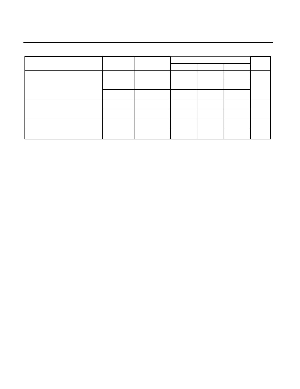
RECOMMENDED OPERATING CONDITIONS
Parameter Symbol
V
CC
Min Typ
2.7
Value
3.0 5.5
Max
MB1501
MB1501H
MB1501L
Unit
V
Power Supply Voltage
Open-drain Output
Input Voltage
Operating temperature
V
VP, V
V
OOP
V
PH
OOPH
, V
V
IN
T
A
PL
OOPL
MB1501H
MB1501
MB1501L
MB1501H
MB1501
MB1501L
V
CC
V
CC
V
CC
V
CC
GND
–40
10.0
8.5
10.0
8.5
V
CC
+85
V
V
V
°C
7
Page 8
MB1501
MB1501H
MB1501L
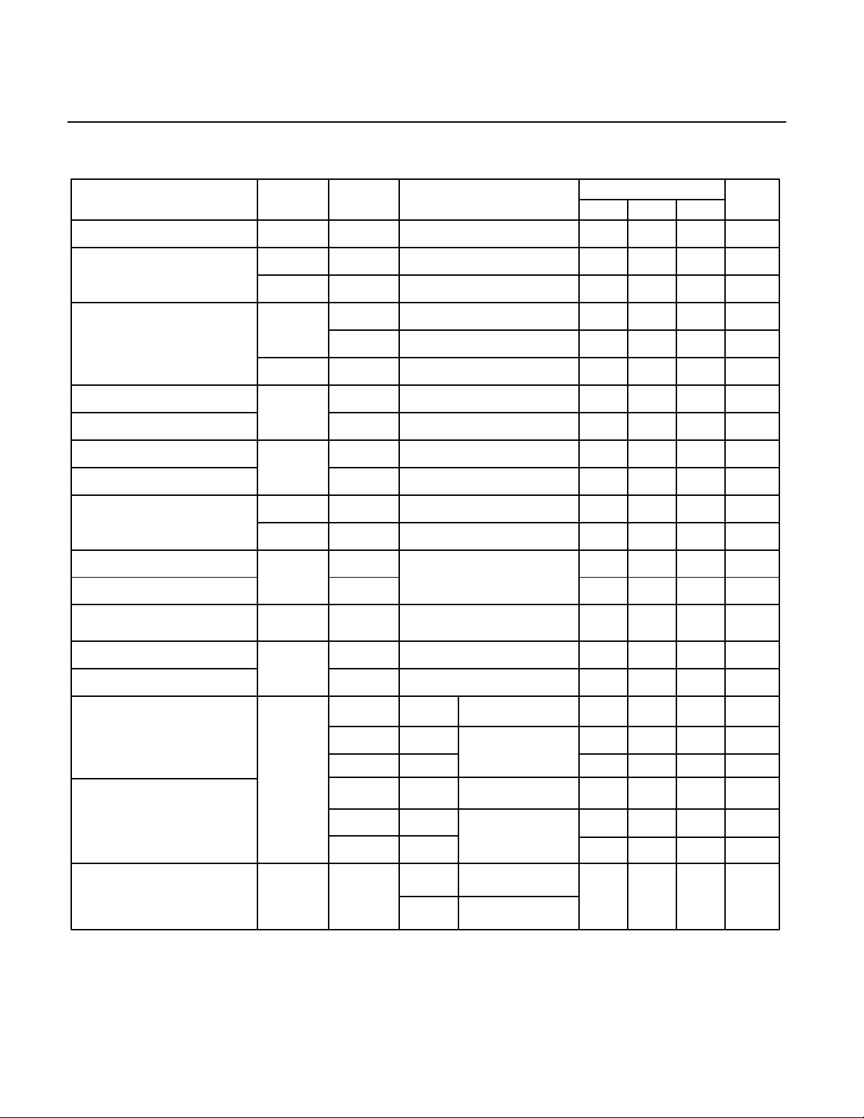
ELECTRICAL CHARACTERISTICS
(VCC=2.7 to 5.5V, TA=–40 to +85°C)
Parameter Symbol
Power Supply Current
Pin Name Condition
V
CC
I
CC
*1
Value
Min Typ Max
——
15 mA
Unit
f
Operating Frequency
Input Sensitivity
High-level Input Voltage
in
OSC
f
in
OSC
Except
IN
IN
fin and
Low-level Input Voltage
High-level Input Current
Low-level Input Current
Input Current
OSC
Data,
Clock
OSC
IN
IN
LE, FC
High-level Output Voltage
Except
DO and
Low-level Output Voltage
N-channel Open-drain
Cutoff Current
High-level Output Current
OSC
ØP
Except
OUT
DO and
Low-level Output Current I
OSC
OUT
High-level Output Current
D
O
Low-level Output Current
Leakage Current
Note: *1 V
=3.0V, fIN=1.1GHz, f
CC
Inputs are grounded except f
*2 Input coupling capacitor 1000pF is connected.
DO, ØP
=12MHz crystal.
OSC
, and outputs are open.
IN
f
IN
f
OSC
P
fin1
P
fin2
V
IN
V
IH
V
IL
I
IH
I
IL
I
IN
I
LE
V
OH
V
OL
I
OFF
I
OH
OL
I
DOHH
I
DOH
I
DOHL
I
DOLH
I
DOL
I
DOLL
IOZ
*2
VCC=2.7 to 4.0V
=4.0 to 5.5V
V
CC
=3.0V
V
CC
V
≤ V
CC
MB1501H
MB1501
MB1501L
MB1501H
MB1501
MB1501L
MB1501H
MB1501
MB1501L
≤ 8V
P
V
V
VCC=3V
V
VCC=3V
V
V
V
V
T
VCC=3V, VP=9V
T
=3V
CC
=12V, TA=25°C
P
=6V, TA=25°C
P
=12V, TA=25°C
P
=3V
CC
=6V, TA=25°C
P
=3V, VP=12V
CC
=25°C
A
=25°C
A
10
—
–10
–4 6
0.5
0.7xV
—
——
——
—
——
2.4
—
12
—
— dBm
——
——
CC
—
1.0
–1.0
±50
–60
——
——
—
–1.0 mA
—
——
——
1100
20
6
MHz
MHz
dBm
V
0.3xV
CC
µA
µA
—
µA
µA
0.4
1.1
µA
mA1.0
P-P
V
V
V
V
mA–2.2 –4.5 —
mA–0.5 –2.0 —
mA–0.5 –1.1 –2.2
—
mA2.2 6.0
mA1.5 6.0 —
mA4.5 12.0 —
— 1.0
µA
8
Page 9
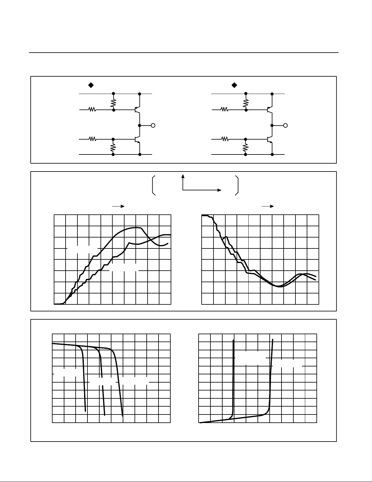
TYPICAL CHARACTERISTICS CURVES
CHARGE PUMP CHARACTERISTICS
MB1501/MB1501H MB1501L
V
P
10kΩ3.6kΩ
MB1501
MB1501H
MB1501L
V
P
10kΩ12kΩ
24.8kΩ
20kΩ
LOCK UP TIME MEASUREMENT
Low unlock condition Lock (533MHz) High unlock condition Lock (518MHz)
MB1501H
MB1501L
D
O
GND
1V/div
10ns/div
12kΩ
10kΩ
D
O
GND
DO PIN OUTPUT CURRENT CURVES (TYPICAL)
VOH vs. I
8.0
7.0
High-level Output Voltage VOH (V)
6.0
0 –1–2–3–4–5
OH
MB1501L
MB1501
High-level Output Current I
MB1501H
(mA)
OH
VOL vs. I
2.0
OL (V)
1.0
Low-level Output Voltage V
0.0
01020
OL
MB1501
MB1501H
Low-level Output Current I
MB1501L
(mA)
OL
9
Page 10
MB1501
MB1501H
MB1501L
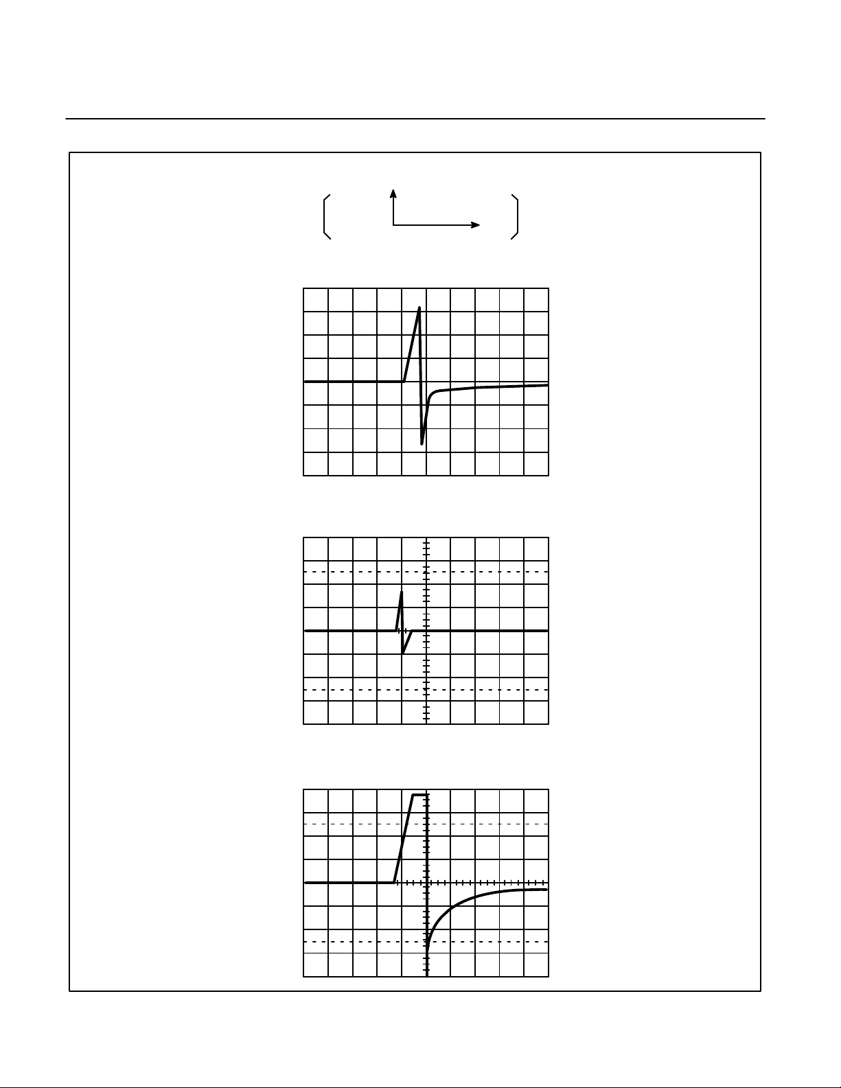
PIN OUTPUT WAVEFORM AT LOCK CONDITION
D
O
Output Waveform
MB1501
1V/div
100ns/div
MB1501H
MB1501L
10
Page 11
MB1501
É
É
MB1501H
MB1501L
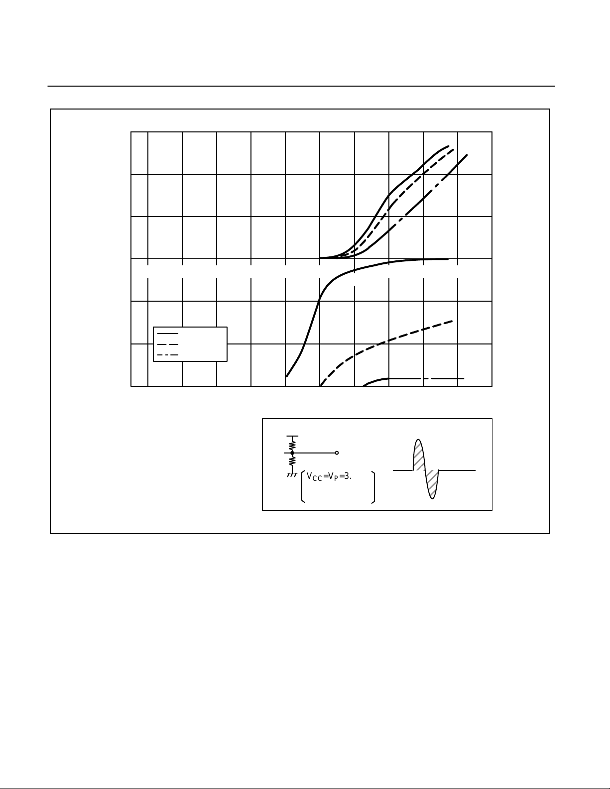
PHASE CHARACTERISTICS (∆f vs. D
150
100
50
t
2
0
100 80 60 40 20 0
Energy (En) – V
–50
–100
–150
MB1501H
MB1501
MB1501L
OUTPUT ENERGY)
O
Time
20
40 60 80
∆f (ns)
V
P
10k
D
O
10k
Oscilloscope
(+) Energy
VCC=VP=3.0V
f
f
INSfOSC
=46.9kHz
r=fP
=12MHz
(–) Energy
11
Page 12
MB1501
MB1501H
MB1501L
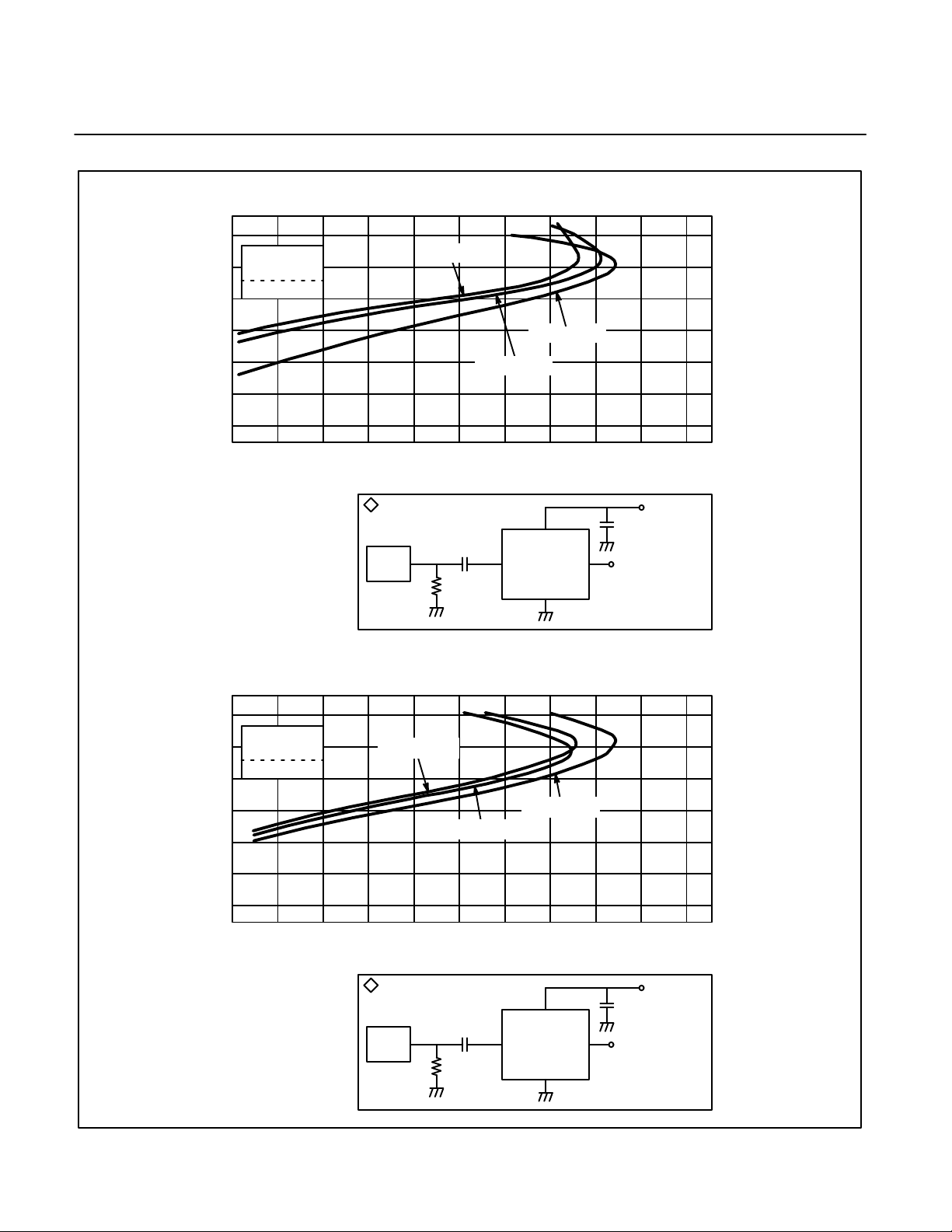
INPUT SENSITIVITY
(dBm)
fIN
Input Sensitivity vs. Input Frequency (Supply Voltage Dependence)
+10
–10
0
Guaranteed
Operating Area
=4.0 to 5.5V
V
CC
VCC=2.7 to 4.0V
VCC=5.5V
–20
–30
Input Sensitivity P
–40
–50
+10
(dBm)
fIN
–10
VCC=2.7V
VCC=4.5V
1.0 1.1 1.2 1.3 1.4 1.5 1.6 1.7 1.8 1.9
Input Frequency fin (GHz)
=25°C
T
A
V
CC
0.1µF
4
814
Oscilloscope
(Counter)
6
P.G
1000pF
50
Ω
Input Sensitivity vs. Input Frequency (Temperature Dependence)
Guaranteed
Operating Area
0
=4.0 to 5.5V
V
CC
VCC=2.7 to 4.0V
TA=–4.0°C
12
–20
–30
–40
Input Sensitivity P
–50
TA=+25°C
TA=+85°C
1.0 1.1 1.2 1.3 1.4 1.5 1.6 1.7 1.8 1.9
Input Frequency fin (GHz)
VCC =3.0V
P.G
1000pF
50
Ω
4
814
6
V
CC
µF
0.1
Oscilloscope
(Counter)
Page 13
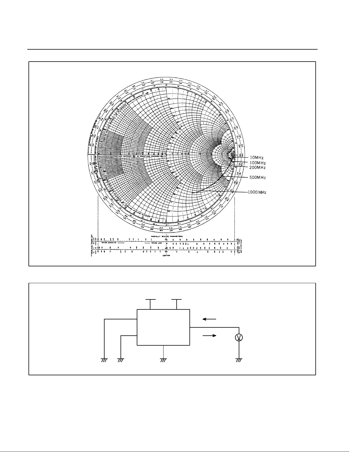
INPUT IMPEDANCE
MB1501
MB1501H
MB1501L
TEST CIRCUIT
DO Pin Output Current (IOH, IOL) Measurement
V
OSC
IN
f
in
CC
MB1501
V
P
D
O
I
OL
I
OH
13
Page 14
MB1501
MB1501H
MB1501L
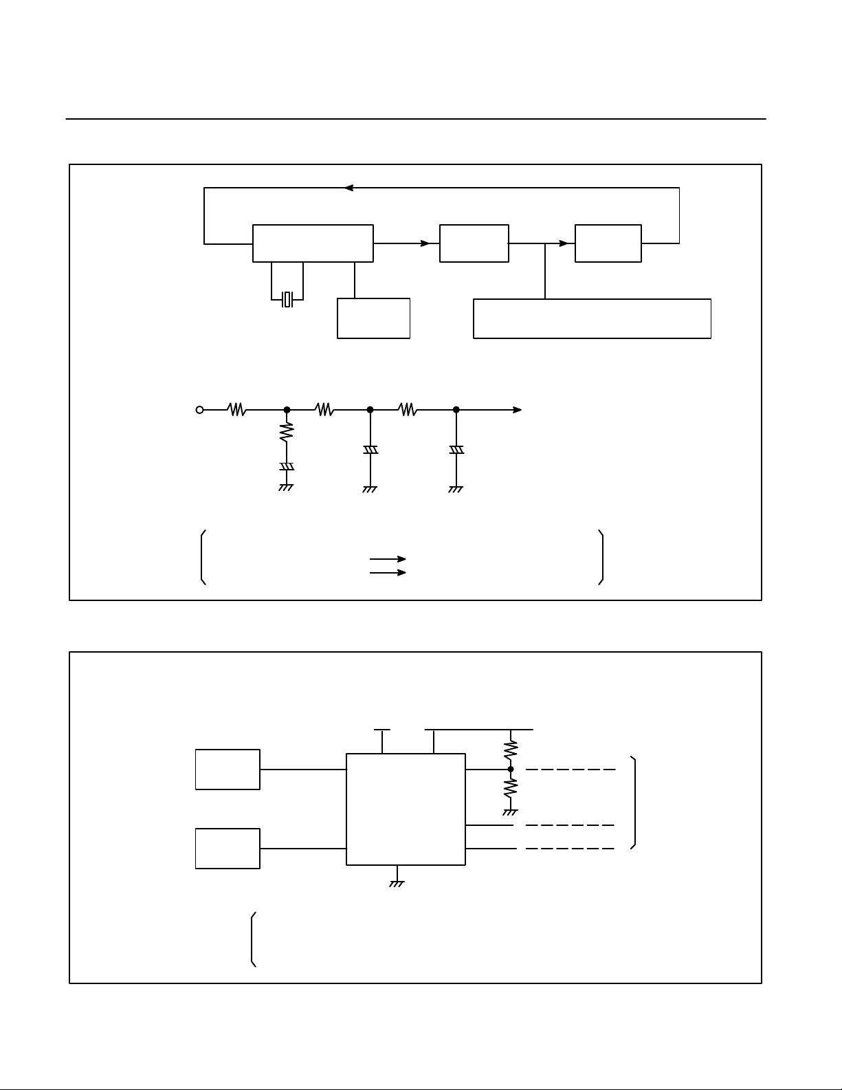
Lock up Time Measurement
f
IN
MB1501
12.8MHz
LPF Circuit
1kΩ 4kΩ 4kΩ
1kΩ
10µF
V
=3V, VP=8V
CC
f
=Low unlock condition Step to Lock condition (533MHz)
VCO
f
=High unlock condition Step to Lock condition (518MHz)
VCO
Phase Characteristics Measurement
D
Controller
(Divide
ratio setting)
0.1
O
LPF
µF1µF
VCO
Oscilloscope (10M
to VCO
Ω, 10pF)
14
⋅ G
P
P ⋅ G
OSCin
fin
V
=3V, VP=3V
CC
∆f=fr–fp
Energy (En)=V
V
CC
MB1501
V
P
D
fr
10kΩ
O
10kΩ
Oscilloscope
(10M
Ω, 10pF)
fp
2
t
Page 15
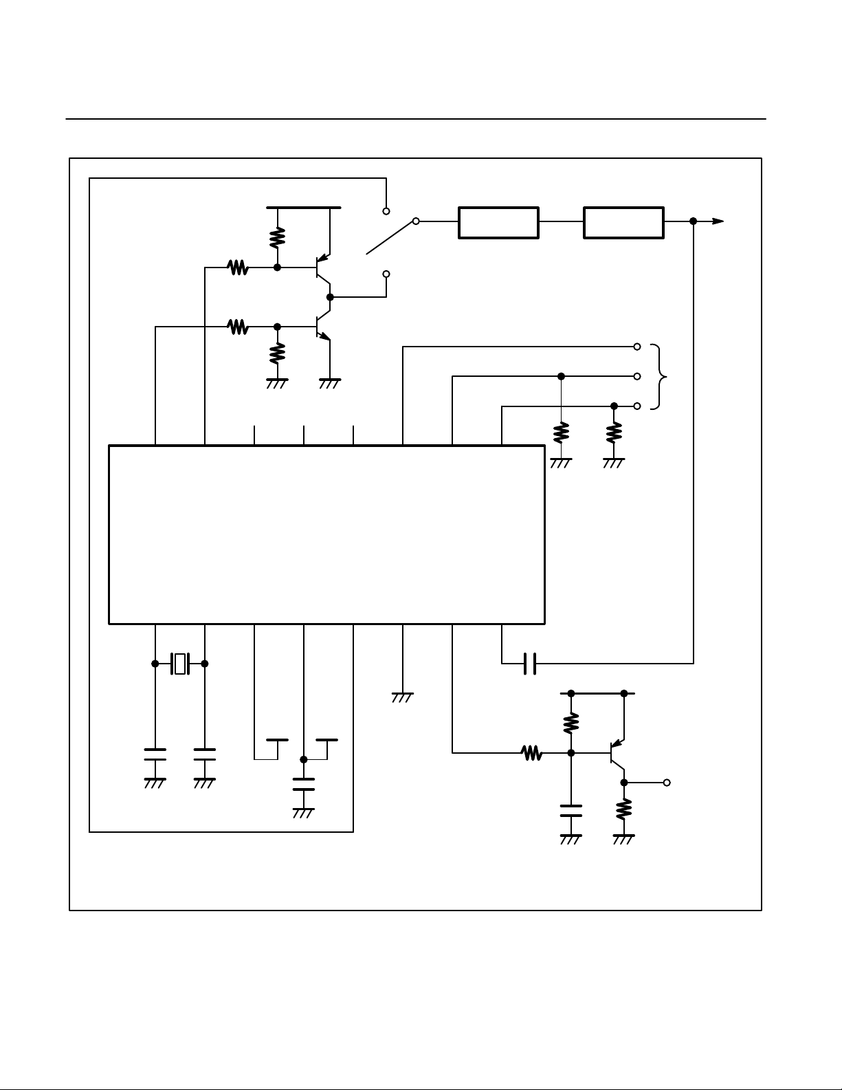
TYPICAL APPLICATION EXAMPLE
(6V)
V
PX
10kΩ
Charge Pump Selection
12kΩ
12kΩ
10kΩ
(Internal or external)
MB1501
MB1501H
MB1501L
OUTPUT
LPF VCO
FROM
CONTROLLER
ØR ØP f
P
f
FC LE Data Clock
r
16 15 14 13 12 11 10 9
MB1501
12345678
OSC
IN
OSC
OUTVp
V
CC
D
GND LD f
O
X’tal
6V 3V
C
C
1
2
0.1µF
IN
1000pF
33k
Ω
0.01µF
47kΩ 47kΩ
V
(3V)
CC
100kΩ
10kΩ
LOCK DET.
, C2: Depends on crystal oscillator
C
1
LE,FC: With internal pull up resistor
ØP : Open drain output
15
Page 16
MB1501
MB1501H
MB1501L
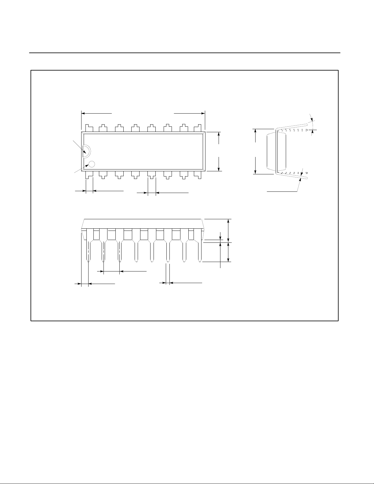
PACKAGE DIMENSIONS
16-LEAD PLASTIC DUAL IN-LINE PACKAGE
(Case No.: DIP-16P-M04)
INDEX-1
INDEX-2
+.012
.039
–0
+0.30
(0.99 )
–0
.050(1.27)
MAX
.770
.100(2.54)
+.008
–.012
TYP
+0.20
(19.55 )
–0.30
.060
(1.52 )
+.012
–0
+0.30
–0
.018
(0.46
±.003
±0.08)
.244
±.010
(6.20
±0.25)
.172(4.36)MAX
.118(3.00)MIN
.020(0.51)MIN
.300(7.62)
TYP
.010
(0.25
±.002
±0.05)
15
°MAX
1991 FUJITSU LIMITED D16033S-2C
16
Dimensions in
inches (millimeters)
Page 17
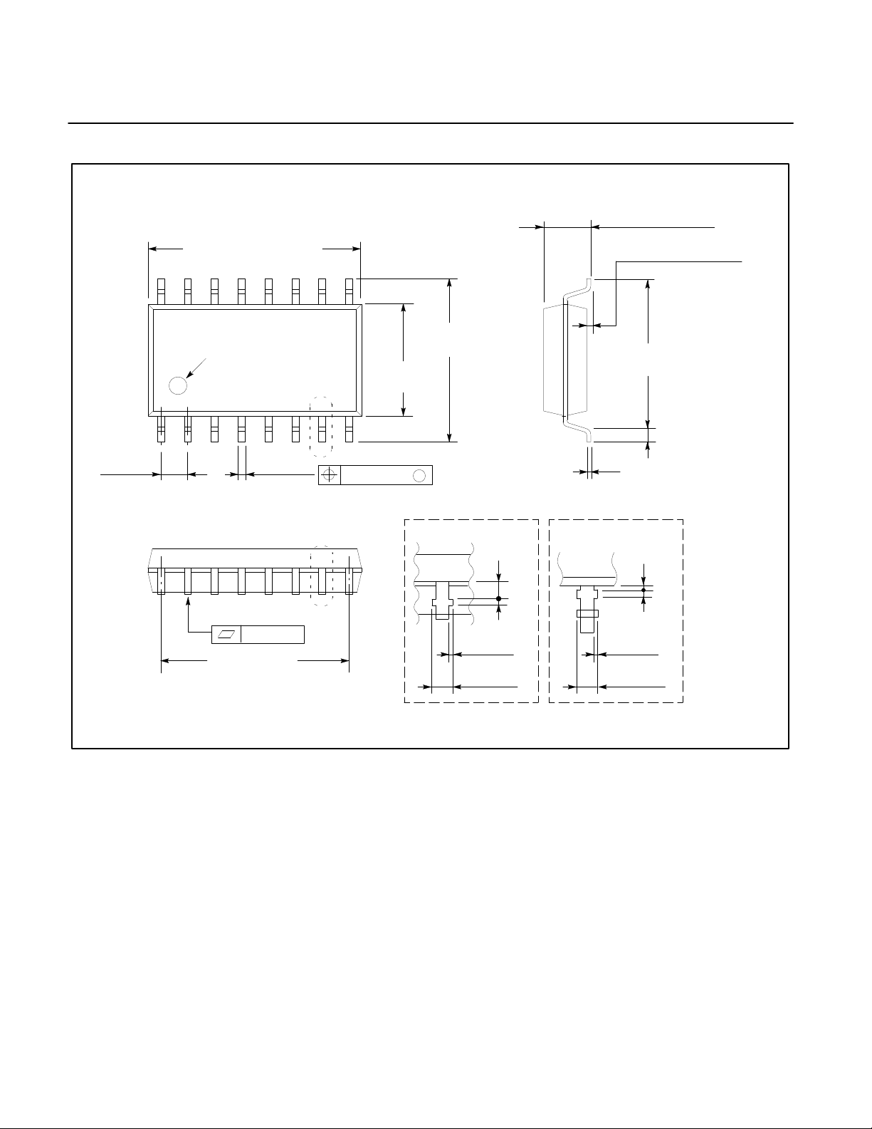
PACKAGE DIMENSIONS
16-LEAD PLASTIC FLAT PACKAGE
(Case No.: FPT-16P-M06)
.050(1.27)
TYP
.400
INDEX
+.010
–.008
+0.25
(10.15 )
–0.20
.018±.004
(0.45
±0.10)
“B”
Ø.005(0.13)
.209
(5.30
(7.80
±.012
±0.30)
M
.307
±.016
±0.40)
.089(2.25)MAX
(MOUNTING HEIGHT)
.002(0.05)MIN
(STAND OFF HEIGHT)
.268
+.016
–.008
.006
+0.40
(6.80 )
–0.20
.020
±.008
(0.50
±0.20)
+.002
(0.15 )
–.001
MB1501
MB1501H
MB1501L
+0.05
–0.02
.004(0.10)
.350(8.89) REF
1991 FUJITSU LIMITED F16015S-2C
“A”
Details of “A” part
.016(0.40)
.008(0.20)
.007(0.18)
MAX
.027(0.68)
MAX
Details of “B” part
.006(0.15)
.008(0.20)
.007(0.18)
MAX
.027(0.68)
MAX
Dimensions in
inches (millimeters)
17
 Loading...