

Page 1
Zener Diodes
MAZ4000 Series (MA4000 Series)
Silicon planar type
For stabilization of power supply
■ Features
•
High reliability, achieved by the DHD structure
•
Allowing to insert to a 5 mm pitch hole
•
Finely divided zener-voltage rank
•
Sharp rising performance
•
Wide voltage range: V
= 2.0 V to 39 V
Z
■ Absolute Maximum Ratings Ta = 25°C
Parameter Symbol Rating Unit
Average forward current I
Repetitive peak forward current I
1
Total power dissipation
*
Non-repetitive reverse surge P
2
power dissipation
*
Junction temperature T
Storage temperature T
Note)*1: With a printed circuit board
2: t = 100 µs, Tj = 150°C
*
F(AV)
FRM
P
tot
ZSM
stg
j
250 mA
250 mA
370 mW
200 °C
−65 to +200 °C
30 W
13 min.
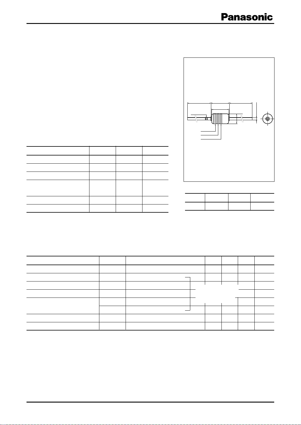
Colored band
indicatesVz
classification
Cathode
1st Band
2nd Band
3rd Band
•
Color indication of VZ rank classification
Rank L M H
Color Black Blue Red
2.7
2.5±0.1
±0.15
13 min.
φ1.55±0.2
Anode
DO-34-A2 Package
Unit: mm
φ 0.40±00.5
1
■ Common Electrical Characteristics Ta = 25°C
*
Parameter Symbol Conditions Min Typ Max Unit
Forward voltage V
2
Zener voltage
*
Zener knee operating resistance R
Zener operating resistance R
Reverse current I
3
Temperature coefficient of zener voltage
*
Terminal capacitance C
V
ZK
R1
I
R2
S
Z
I
F
Z
Z
t
= 10 mA 0.8 0.9 V
F
I
Z
I
Z
I
Z
V
V
I
Z
V
Specified value V
Specified value Ω
Specified value Ω
Specified value µA
R
Specified value µA
R
Specified value mV/°C
Specified value pF
R
Note) 1.Rated input/output frequency: 5 MHz
2.
1 : The V
*
2 : Guaranteed at 20 ms after power application.
*
3:T
*
value is for the temperature of 25°C. In other cases, carry out the temperature compensation.
Z
= 25°C to 150°C
j
Note) The part number in the parenthesis shows conventional part number.
Publication date: February 2002 SKE00004CED
Refer to the list of the
electrical characteristics
within part numbers
1
Page 2
MAZ4000 Series
■ Electrical characteristics within part numbers Ta = 25°C
•
V
= 2.0 V to 6.8 V (IZ = 5 mA)
Z
Temperature
coefficient of
zener voltage
I
= 5 mA
Z
Max Min Typ Max
Part number
Zener voltage Reverse current
VZ (V) I
I
= 5 mA V
Z
(µA) IR2 (µA) RZ (Ω)RZK (Ω)SZ (mV/°C)
R1
V
R
R
Zener operating
resistance
I
= 5 mA I
Z
Min Nom Max (V) Max (V) Max Typ Max
Z
(mA)
MAZ4020 1.88 2.24
MAZ40200L 1.88 2.12 0.5 120 100 1 2000 −3.5 −1.5 0 375 450 Red Black Black
MAZ40200H 2.01 2.24
MAZ4022 2.08 2.45
MAZ40220L 2.08 2.33 0.7 120 100 1 2000 −3.5 −1.5 0 375 450 Red Red Red
MAZ40220H 2.20 2.45
MAZ4024 2.28 2.4 2.7
MAZ40240L 2.28 2.56 1 120 100 1 2000 −3.5 −1.6 0 375 450 Red Yellow Yellow
MAZ40240H 2.4 2.7
MAZ4027 2.5 2.7 2.9
MAZ40270L 2.5 2.75 1 100 100 1 1000 −3.5 −2 0 350 450 Red Purple Purple
MAZ40270H 2.65 2.9
MAZ4030 2.8 3.0 3.2
MAZ40300L 2.83 2.9 2.97
MAZ40300M 2.93 3.0 3.08
15085 100 1 1000 −3.5 −2.1 0 350 450 Orange Black Black
MAZ40300H 3.02 3.1 3.18
MAZ4033 3.1 3.3 3.5
MAZ40330L 3.12 3.2 3.28
MAZ40330M 3.22 3.3 3.38
12083 100 1 1000 −3.5 −2.4 0 325 450 Orange Orange Orange
MAZ40330H 3.32 3.4 3.49
MAZ4036 3.4 3.6 3.8
MAZ40360L 3.41 3.5 3.59
MAZ40360M 3.51 3.6 3.69
11081 100 1 1000 −3.5 −2.4 0 300 450 Orange Blue Blue
MAZ40360H 3.61 3.7 3.79
MAZ4039 3.7 3.9 4.1
MAZ40390L 3.71 3.8 3.9
MAZ40390M 3.8 3.9 4.0
11079 100 1 1000 −3.5 −2.5 0 300 450 Orange White White
MAZ40390H 3.9 4.0 4.1
MAZ4043 4.0 4.3 4.6
MAZ40430L 4.03 4.1 4.26
MAZ40430M 4.17 4.3 4.4
11075 100 1 1000 −3.5 −2.5 0 275 450 Yellow Orange Orange
MAZ40430H 4.31 4.4 4.54
MAZ4047 4.4 4.7 5.0
MAZ40470L 4.45 4.6 4.69
MAZ40470M 4.59 4.7 4.83
1350 80 1 900 −3.5 −1.4 0.2 130 180 Yellow Purple Purple
MAZ40470H 4.74 4.9 4.99
MAZ4051 4.8 5.1 5.4
MAZ40510L 4.87 5.0 5.12
MAZ40510M 5.0 5.1 5.26
2240 60 1 800 −2.7 0.8 1.2 110 160 Green Brown Brown
MAZ40510H 5.14 5.3 5.4
MAZ4056 5.3 5.6 6.0
MAZ40560L 5.3 5.4 5.58
MAZ40560M 5.48 5.6 5.76
2115 40 1 500 −2 1.2 2.5 95 140 Green Blue Blue
MAZ40560H 5.66 5.8 5.95
MAZ4062 5.8 6.2 6.6 5.3
MAZ40620L 5.85 6.0 6.15
MAZ40620M 6.05 6.2 6.36 5.5
43
5.3
60 6 20 0.5 300 0.4 2.3 3.7 90 130 Blue Red Red
MAZ40620H 6.24 6.4 6.56 5.7
MAZ4068 6.4 6.8 7.2 5.9
MAZ40680L 6.44 6.6 6.77
MAZ40680M 6.64 6.8 6.98 6.1
42
5.9
60 6 15 0.5 140 1.2 3 4.5 85 110 Blue Gray Gray
MAZ40680H 6.85 7.0 7.2 6.3
Terminal
capaci-
tance
Ct (pF)
= 0 V)
(V
R
f = 1 MHz
Typ Max
Marking symbol
Color indication
Main body:
Yellowish green
1st. 2nd. 3rd.
2
SKE00004CED
Page 3
MAZ4000 Series
■ Electrical characteristics within part numbers (continued) Ta = 25°C
•
V
= 7.5 V to 20 V (IZ = 5 mA)
Z
Temperature
coefficient of
zener voltage
I
= 5 mA
Z
Max Min Typ Max
Part number
Zener voltage Reverse current
VZ (V) I
I
= 5 mA V
Z
(µA) IR2 (µA) RZ (Ω)RZK (Ω)SZ (mV/°C)
R1
V
R
R
Zener operating
resistance
I
= 5 mA
Z
Min Nom Max (V) Max (V) Max Typ Max
I
Z
(mA)
MAZ4075 7.0 7.5 7.9 6.5
MAZ40750L 7.07 7.3 7.43
MAZ40750M 7.29 7.5 7.67 6.7
51
6.5
60 6 15 0.5 120 2.5 4 5.3 80 100 Purple Green Green
MAZ40750H 7.51 7.7 7.89 7.0
MAZ4082 7.7 8.2 8.7 7.2
MAZ40820L 7.77 7.9 8.17
MAZ40820M 8.03 8.2 8.43 7.5
5 0.5
7.2
60 6 15 0.5 120 3.2 4.6 6.2 75 95 Gray Red Red
MAZ40820H 8.29 8.5 8.7 7.7
MAZ4091 8.5 9.1 9.6 8
MAZ40910L 8.58 8.8 9.02
MAZ40910M 8.87 9.1 9.33 8.3
6 0.2
8
60 6 15 0.5 130 3.8 5.5 7 70 90 White Brown Brown
MAZ40910H 9.14 9.4 9.6 8.6
MAZ4100 9.4 10 10.6 8.9
MAZ41000L 9.44 9.7 9.92
MAZ41000M 9.75 10 10.25 9.2
7 0.2
8.9
60 8 20 0.5 130 4.5 6.4 8 70 90 Brown Black
MAZ41000H 10.07 10.3 10.59 9.5
MAZ4110 10.4 11 11.6 9.9
MAZ41100L 10.4 10.7 10.94
MAZ41100M 10.73 11 11.28 10.2
7 0.1
9.9
60 10 20 0.5 170 5.4 7.4 9 65 85 Brown Brown
MAZ41100H 11.05 11.3 11.6 10.5
MAZ4120 11.4 12 12.7 10.9
MAZ41200L 11.4 11.7 11.96
MAZ41200M 11.73 12 12.33 11.2
8 0.1
10.9
60 10 25 0.5 170 6 8.4 10 65 85 Brown Red
MAZ41200H 12.06 12.3 12.68 11.5
MAZ4130 12.4 13 14.1 11.9
MAZ41300L 12.4 12.7 12.99
MAZ41300M 12.73 13 13.4 12.2
9 0.1
11.9
60 10 30 0.5 170 7 9.4 11 60 80 Brown Orange
MAZ41300H 13.25 13.7 14.08 12.7
MAZ41400M 13.65 14 14.35 9 0.1 13.1 60 10 30 0.5 170 7 10 13 60 80 Brown Yellow
MAZ4150 13.9 15 15.6 13.4
MAZ41500L 13.9 14.3 14.76
MAZ41500M 14.6 15 15.35 14.1
10 0.05
13.4
60 10 30 0.5 170 9.2 11.4 13 55 75 Brown Green
MAZ41500H 14.95 15.3 15.6 14.4
MAZ4160 15.3 16 17.1 14.8
MAZ41600L 15.3 15.7 16.09
MAZ41600M 15.7 16 16.5 15.2
11 0.05
14.8
60 10 40 0.5 170 10.4 12.4 14 52 75 Brown Blue
MAZ41600H 16.26 16.7 17.1 15.7
MAZ4180 16.9 18 19.1 16.4
MAZ41800L 16.9 17.3 17.76
MAZ41800M 17.55 18 18.45 17
13 0.05
16.4
60 10 45 0.5 170 12.4 14.4 16 47 70 Brown Gray
MAZ41800H 18.2 18.7 19.1 17.7
MAZ4200 18.8 20 21.2 18.3
MAZ42000L 18.85 19.3 19.81
MAZ42000M 19.50 20 20.5 19
14 0.05
18.3
60 15 55 0.5 180 14.4 16.4 18 36 60 Red Black
MAZ42000H 20.15 20.7 21.19 19.6
Terminal
capaci-
tance
Ct (pF)
= 0 V)
(V
R
f = 1 MHz
Typ Max
Marking symbol
Color indication
Main body:
Yellowish green
1st. 2nd. 3rd.
SKE00004CED
3
Page 4

MAZ4000 Series
■ Electrical characteristics within part numbers (continued) Ta = 25°C
•
V
= 22.0 V to 24.0 V (IZ = 5 mA)
Z
Zener operating
resistance
I
= 5 mA
Z
Part number
Zener voltage Reverse current
VZ (V) I
I
= 5 mA V
Z
(µA) IR2 (µA) RZ (Ω)RZK (Ω)SZ (mV/°C)
R1
V
R
R
Min Nom Max (V) Max (V) Max Typ Max
MAZ4220 20.8 22 23.3 20.3
MAZ4220-L 20.8 21.3 21.86
MAZ4220-M 21.45 22 22.55 20.9
15 0.05
20.3
60 20 5.5 0.5 180 16.4 18.4 20 34 60 Red Red
MAZ4220-H 22.1 22.7 23.24 21.6
MAZ4240 22.8 24 25.6 22.3
MAZ4240-L 22.8 23.3 23.97
MAZ4240-M 23.5 24 24.7 23
17 0.05
22.3
60 25 70 0.5 180 18.4 20.4 22 33 55 Red Yellow
MAZ4240-H 24.35 25 25.6 23.8
•
V
= 27.0 V to 39.0 V (IZ = 2 mA)
Z
Zener operating
resistance
I
= 2 mA
Z
Part number
Zener voltage Reverse current
VZ (V) I
I
= 2 mA V
Z
(µA) IR2 (µA) RZ (Ω)RZK (Ω)SZ (mV/°C)
R1
V
R
R
Min Nom Max (V) Max (V) Max Typ Max
MAZ4270 25.1 27 28.9 24.8
MAZ42700L 25.3 26 26.7
MAZ42700M 26.3 27 27.7 25.8
19 0.05
24.8
60 25 80 0.5 200 21.4 23.4 25.3 30 50 Red Purple
MAZ42700H 27.3 28 28.7 26.8
MAZ4300 28 30 32 27.8
MAZ43000L 28.3 29 29.7
MAZ43000M 29.3 30 30.8 28.8
21 0.05
27.8
60 30 80 0.5 200 24.4 26.6 29.4 27 50 Orange Black
MAZ43000H 30.2 31 31.8 29.7
MAZ4330 31 33 35 30.7
MAZ43300L 31.2 32 32.8
MAZ43300M 32.2 33 33.8 31.7
23 0.05
30.7
60 35 80 0.5 200 27.4 29.7 33.4 25 45 Orange Orange
MAZ43300H 33.2 34 34.9 32.7
MAZ4360 34 36 38 33.6
MAZ43600L 34.1 35 35.9
MAZ43600M 35.1 36 36.9 34.6
25 0.05
33.6
60 35 90 0.5 200 30.4 33 37.4 23 45 Orange Blue
MAZ43600H 36.1 37 37.9 35.6
MAZ4390 37 41 36
MAZ43900L 37.1 39
MAZ43900M 38 40 36
27 0.05
36
60 130 0.5 250 33.4 36.4 41.2 21 45 Orange White
MAZ43900H 39 41 36
Note) 1. The VZ value is the one after power application for 20 ms at T
2. The zener voltage temperature coefficient is the one for T
= 25°C to 150°C.
j
I
Z
(mA)
I
Z
(mA)
= 25°C.
a
Temperature
coefficient of
zener voltage
I
= 5 mA
Z
Max Min Typ Max
Temperature
coefficient of
zener voltage
I
= 2 mA
Z
Max Min Typ Max
Terminal
capaci-
tance
Ct (pF)
= 0 V)
(V
R
f = 1 MHz
Typ Max
Terminal
capaci-
tance
Ct (pF)
= 0 V)
(V
R
f = 1 MHz
Typ Max
Marking symbol
Color indication
Main body:
Yellowish green
1st. 2nd. 3rd.
Marking symbol
Color indication
Main body:
Yellowish green
1st. 2nd. 3rd.
4
SKE00004CED
Page 5

P
T
500
400
)
mW
(
tot
300
200
Power dissipation P
100
0
0 25020015010050
tot
Thickness of the printed-circuit board 1.6 mm
Copper foil 0.035 mm, Hole distance 5 mm
Anode side copper foil φ 3 mm
Cathode side copper foil φ 3 mm
Ambient temperature Ta (°C
I
V
160
120
)
mA
(
Z
80
Zener current I
40
Z
MAZ4024
MAZ4027
MAZ4030
MAZ4033
MAZ4036
MAZ4039
MAZ4043
a
Z
Ta = 25°C
Static
Characteristics
MAZ4000 Series
P
t
ZSM
I
Z
V
W
)
)
Z
Ta = 25°C
Static
Characteristics
)
500
)
W
300
(
200
ZSM
100
50
30
20
10
5
3
2
Non-repetitive reverse surge power dissipation P
1
0.1 0.3 3
)
120
100
Ta = 25°C (Prior to surge
150°C (Prior to surge
0.5 51100.2 2
Pulse width tW (ms
)
80
mA
(
Z
60
40
Zener current I
20
MAZ4047
MAZ4051
MAZ4056
MAZ4062
MAZ4068
MAZ4075
MAZ4082
MAZ4091
MAZ4100
320
280
)
240
mA
(
200
F
160
120
Forward current I
80
40
0
0 0.2 0.4 0.6 0.8 1.0 1.2
40
30
)
mA
(
Z
20
Zener current I
10
I
V
F
F
Ta = 25°C
Forward voltage VF (V
I
V
Z
Z
Ta = 25°C
Static
Characteristics
MAZ4110
MAZ4130
MAZ4160
MAZ4200
MAZ4240
)
MAZ4270
MAZ4300
MAZ4330
MAZ4360
0
0615234
Zener voltage VZ (V
I
V
Z
200
Tj = 25°C
Dynamic
Characteristics
160
)
mA
(
120
Z
80
Zener current I
40
0
MAZ4024
MAZ4027
MAZ4030
MAZ4033
MAZ4036
MAZ4039
MAZ4043
0123456
Z
Zener voltage VZ (V
0
)
)
024681012
Zener voltage VZ (V
I
V
Z
MAZ4062
MAZ4047
Z
MAZ4082
200
Tj = 25°C
180
Dynamic
Characteristics
160
)
140
mA
(
120
Z
100
80
60
Zener current I
40
20
0
024681012
MAZ4056
MAZ4051
Zener voltage VZ (V
)
MAZ4100
MAZ4091
)
MAZ4068 MAZ4075
SKE00004CED
0
010 3020 40
Zener voltage VZ (V
I
V
Z
100
80
Z
Tj = 25°C
Dynamic
Characteristics
)
mA
(
60
Z
MAZ4240
MAZ4200
MAZ4160
MAZ4130
MAZ4110
40
Zener current I
20
0
010 3020 40
Zener voltage VZ (V
)
MAZ4300
MAZ4270
)
MAZ4360
MAZ4330
5
Page 6

MAZ4000 Series
3
)
1
°C / mW
(
th
0.3
0.1
Thermal impedance Z
0.03
0.1 1003010310.3
Z
t
th
W
Pulse width tW (s
Heat sink
Thickness t = 1.6 mm
Copper foil t = 0.035 mm
Anode side φ 3 mm
Cathode side φ 3 mm
Lead distance 5 mm
)
R
I
4
10
)
Ω
(
3
Z
10
2
10
10
Z
Zener operating resistance R
1
−1
10
11010
Zener current IZ (mA
Z
MAZ4033
MAZ4024
MAZ4300
MAZ4047
MAZ4200
MAZ4120
MAZ4068
2
)
I
S
Z
1
)
mV / °C
(
Z
0
S
−1
−2
Temperature coefficient of zener voltage
−3
0 20 40 60 80 100 120
Zener current IZ (mA
Z
T
= 25°C to 150°C
j
MAZ4043
MAZ4024
MAZ4027
MAZ4039
MAZ4036
MAZ4033
MAZ4030
)
S
I
Z
MAZ4000
MAZ4091
MAZ4082
MAZ4075
MAZ4062
MAZ4056
MAZ4047
Z
T
= 25°C to 150°C
j
MAZ4068
MAZ4051
)
10
)
8
mV / °C
(
Z
6
S
4
2
0
−2
−4
Temperature coefficient of zener voltage
−6
04812162024
Zener current IZ (mA
6
SKE00004CED
Page 7

Request for your special attention and precautions in using the technical information
and semiconductors described in this material
(1) An export permit needs to be obtained from the competent authorities of the Japanese Govern-
ment if any of the products or technologies described in this material and controlled under the
"Foreign Exchange and Foreign Trade Law" is to be exported or taken out of Japan.
(2) The technical information described in this material is limited to showing representative character-
istics and applied circuit examples of the products. It does not constitute the warranting of industrial
property, the granting of relative rights, or the granting of any license.
(3) The products described in this material are intended to be used for standard applications or gen-
eral electronic equipment (such as office equipment, communications equipment, measuring instruments and household appliances).
Consult our sales staff in advance for information on the following applications:
• Special applications (such as for airplanes, aerospace, automobiles, traffic control equipment,
combustion equipment, life support systems and safety devices) in which exceptional quality and
reliability are required, or if the failure or malfunction of the products may directly jeopardize life or
harm the human body.
• Any applications other than the standard applications intended.
(4) The products and product specifications described in this material are subject to change without
notice for reasons of modification and/or improvement. At the final stage of your design, purchasing, or use of the products, therefore, ask for the most up-to-date Product Standards in advance to
make sure that the latest specifications satisfy your requirements.
(5) When designing your equipment, comply with the guaranteed values, in particular those of maxi-
mum rating, the range of operating power supply voltage and heat radiation characteristics. Otherwise, we will not be liable for any defect which may arise later in your equipment.
Even when the products are used within the guaranteed values, redundant design is recommended,
so that such equipment may not violate relevant laws or regulations because of the function of our
products.
(6) When using products for which dry packing is required, observe the conditions (including shelf life
and after-unpacking standby time) agreed upon when specification sheets are individually exchanged.
(7) No part of this material may be reprinted or reproduced by any means without written permission
from our company.
Please read the following notes before using the datasheets
A. These materials are intended as a reference to assist customers with the selection of Panasonic
semiconductor products best suited to their applications.
Due to modification or other reasons, any information contained in this material, such as available
product types, technical data, and so on, is subject to change without notice.
Customers are advised to contact our semiconductor sales office and obtain the latest information
before starting precise technical research and/or purchasing activities.
B. Panasonic is endeavoring to continually improve the quality and reliability of these materials but
there is always the possibility that further rectifications will be required in the future. Therefore,
Panasonic will not assume any liability for any damages arising from any errors etc. that may appear in this material.
C. These materials are solely intended for a customer's individual use.
Therefore, without the prior written approval of Panasonic, any other use such as reproducing,
selling, or distributing this material to a third party, via the Internet or in any other way, is prohibited.
2001 MAR
Page 8

WWW.ALLDATASHEET.COM
Copyright © Each Manufacturing Company.
All Datasheets cannot be modified without permission.
This datasheet has been download from :
www.AllDataSheet.com
100% Free DataSheet Search Site.
Free Download.
No Register.
Fast Search System.
www.AllDataSheet.com
 Loading...