

Page 1
19-1229; Rev 6; 8/12
For pricing, delivery, and ordering information, please contact Maxim Direct
at 1-888-629-4642, or visit Maxim’s website at www.maximintegrated.com.
MAX985/MAX986/MAX989/
MAX990/MAX993/MAX994
Micropower, Low-Voltage, UCSP/SC70,
Rail-to-Rail I/O Comparators
General Description
The MAX985/MAX986/MAX989/MAX990/MAX993/
MAX994 single/dual/quad micropower comparators
feature low-voltage operation and rail-to-rail inputs and
outputs. Their operating voltages range from 2.5V to
5.5V, making them ideal for both 3V and 5V systems.
These comparators also operate with ±1.25V to ±2.75V
dual supplies. They consume only 11µA of supply current while achieving a 300ns propagation delay.
Input bias current is typically 1.0pA, and input offset
voltage is typically 0.5mV. Internal hysteresis ensures
clean output switching, even with slow-moving input
signals.
The output stage’s unique design limits supply-current
surges while switching, virtually eliminating the supply
glitches typical of many other comparators. The
MAX985/MAX989/MAX993 have a push-pull output
stage that sinks as well as sources current. Large internal output drivers allow rail-to-rail output swing with
loads up to 8mA. The MAX986/MAX990/MAX994 have
an open-drain output stage that can be pulled beyond
VCCto 6V (max) above VEE. These open-drain versions
are ideal for level translators and bipolar to singleended converters.
The single MAX985 is available in a chip-scale package (UCSP™), significantly reducing the required PC
board area. The single MAX985/MAX986 are available
in 5-pin SC70 packages and the dual MAX989/MAX990
are available in 8-pin SOT23 packages.
____________________________Features
o 11µA Quiescent Supply Current
o 2.5V to 5.5V Single-Supply Operation
o Common-Mode Input Voltage Range Extends
250mV Beyond the Rails
o 300ns Propagation Delay
o Push-Pull Output Stage Sinks and Sources
8mA Current (MAX985/MAX989/MAX993)
o Open-Drain Output Voltage Extends Beyond V
CC
(MAX986/MAX990/MAX994)
o Unique Output Stage Reduces Output Switching
Current, Minimizing Overall Power Consumption
o 80µA Supply Current at 1MHz Switching
Frequency
o No Phase Reversal for Overdriven Inputs
o Available in Space-Saving Packages:
UCSP (MAX985)
SOT23 (MAX985/MAX986/MAX989/MAX990)
µMAX
®
(MAX989/MAX990)
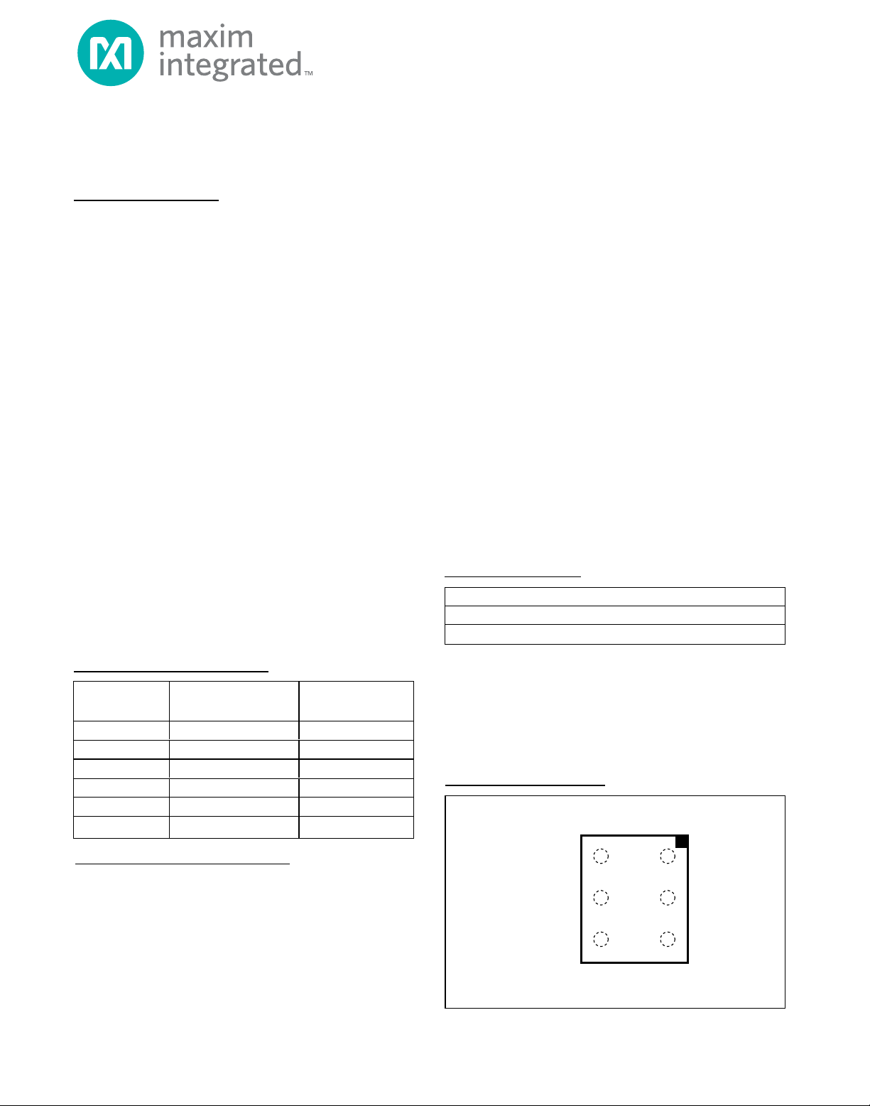
Pin Configurations
Ordering Information
Ordering Information continued at end of data sheet.
Typical Application Circuit appears at end of data sheet.
Pin Configurations continued at end of data sheet.
Portable/BatteryPowered Systems
Mobile Communications
Zero-Crossing Detectors
Window Comparators
Level Translators
Threshold Detectors/
Discriminators
Ground/Supply-Sensing
Applications
IR Receivers
Digital Line Receivers
Applications
Selector Guide
UCSP is a trademark and µMAX is a registered trademark of
Maxim Integrated Products, Inc.
Note: All devices are specified over the -40°C to +85°C operating
temperature range.
+
Denotes a lead(Pb)-free/RoHS-compliant package.
T = Tape and reel.
G45 = Protective die coating.
PART
MAX985 1 Push-Pull
MAX986 1 Open-Drain
MAX989 2 Push-Pull
MAX990 2 Open-Drain
MAX993 4 Push-Pull
MAX994 4 Open-Drain
COMPARATORS
PER PACKAGE
OUTPUT
STAGE
PART PIN-PACKAGE TOP MARK
MAX985EBT+TG45 6 UCSP
MAX985EXK+T 5 SC70
AAY
ABK
TOP VIEW
(BUMPS ON BOTTOM)
IN+
N.C.
B1
B2
B3
MAX985
UCSP
IN-
V
A1
EE
OUT
A2
V
A3
CC
Page 2
MAX985/MAX986/MAX989/
MAX990/MAX993/MAX994
Micropower, Low-Voltage, UCSP/SC70,
Rail-to-Rail I/O Comparators
2
Maxim Integrated
ABSOLUTE MAXIMUM RATINGS
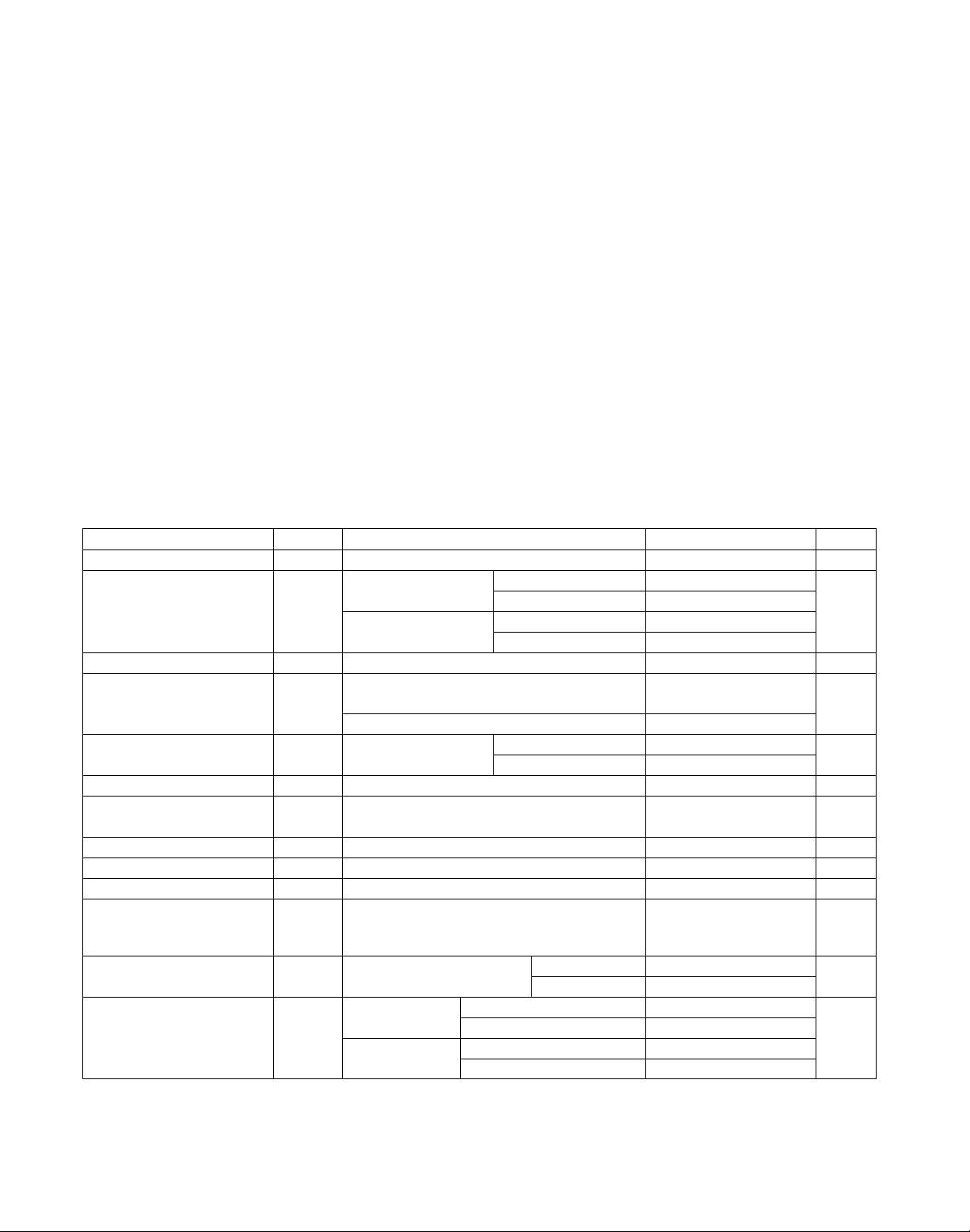
ELECTRICAL CHARACTERISTICS
(VCC= 2.7V to 5.5V, VEE= 0V, VCM= 0V, TA= -40°C to +85°C, unless otherwise noted. Typical values are at TA= +25°C.) (Note 1)
Stresses beyond those listed under “Absolute Maximum Ratings” may cause permanent damage to the device. These are stress ratings only, and functional
operation of the device at these or any other conditions beyond those indicated in the operational sections of the specifications is not implied. Exposure to
absolute maximum rating conditions for extended periods may affect device reliability.
Supply Voltage (VCCto VEE) ...................................................6V
Current into Input Pins ......................................................±20mA
IN_-, IN_+ to V
EE
.......................................-0.3V to (VCC+ 0.3V)
OUT_ to V
EE
MAX985/MAX989/MAX993 ....................-0.3V to (VCC+ 0.3V)
MAX986/MAX990/MAX994.....................................-0.3V to 6V
OUT_ Short-Circuit Duration to V
EE
or VCC...........................10s
Continuous Power Dissipation (Multilayer board, T
A
= +70°C)
5-Pin SC70 (derate 3.1mW/°C above +70°C)...............247mW
5-Pin SOT23 (derate 3.9mW/°C above +70°C)..........312.6mW
6-Bump UCSP (derate 3.9mW/°C above +70°C)..........308mW
8-Pin SOT23 (derate 5.1mW/°C above +70°C)..........408.2mW
8-Pin µMAX (derate 4.8mW/°C above +70°C) ...........387.8mW
8-Pin SO (derate 7.4mW/°C above +70°C)................588.2mW
14-Pin TSSOP (derate 10mW/°C above +70°C) ........796.8mW
14-Pin SO (derate 11.9mW/°C above +70°C)............952.4mW
Operating Temperature Range ...........................-40°C to +85°C
Junction Temperature......................................................+150°C
Storage Temperature Range .............................-65°C to +150°C
Lead Temperature (except UCSP, soldering, 10s)..........+300°C
Soldering Temperature (reflow) ......................................+260°C
Inferred from PSRR test
CONDITIONS
V2.5 5.5V
CC
Supply Voltage
UNITSMIN TYP MAXSYMBOLPARAMETER
12 20
2.5V ≤ VCC≤ 5.5V dB55 80PSRRPower-Supply Rejection Ratio
VCC= 5V
24
mV
±0.5 ±5
TA= +25°C
VEE-V
CC
+
0.25 0.25
±3V
HYST
Input Hysteresis
Full common-mode
range
nAI
B
Input Bias Current
(Note 4)
0.001 10
pF1.0C
IN
Input Capacitance
dB52 80CMRRCommon-Mode Rejection Ratio
pA0.5I
OS
Input Offset Current
±7
V
OS
Input Offset Voltage
(Note 3)
V
OUT
= high µA1.0I
LEAK
Output Leakage Current
(MAX986/MAX990/
MAX994 only)
35
95
TA= +25°C
TA= -40°C to +85°C
11 20
VCC= 2.7V
µA
24
I
CC
Supply Current per
Comparator
TA= +25°C
TA= -40°C to +85°C
Sourcing or sinking,
V
OUT
= V
EE
or V
CC
I
SC
Output Short-Circuit Current
TA= +25°C
TA= -40°C to +85°C
TA= -40°C to +85°C V
EE
V
CC
VV
CMR
Common-Mode Voltage
Range (Note 2)
mV
VCC= 5V
VCC= 2.7V
mA
VCC= 5V,
I
SINK
= 8mA
0.55
0.2 0.4
V
OL
OUT Output Voltage Low
VCC= 2.7V,
I
SINK
= 3.5mA
V
0.4
0.15 0.3
TA= +25°C
TA= -40°C to +85°C
TA= +25°C
TA= -40°C to +85°C
Page 3
3
Maxim Integrated
MAX985/MAX986/MAX989/
MAX990/MAX993/MAX994
Micropower, Low-Voltage, UCSP/SC70,
Rail-to-Rail I/O Comparators
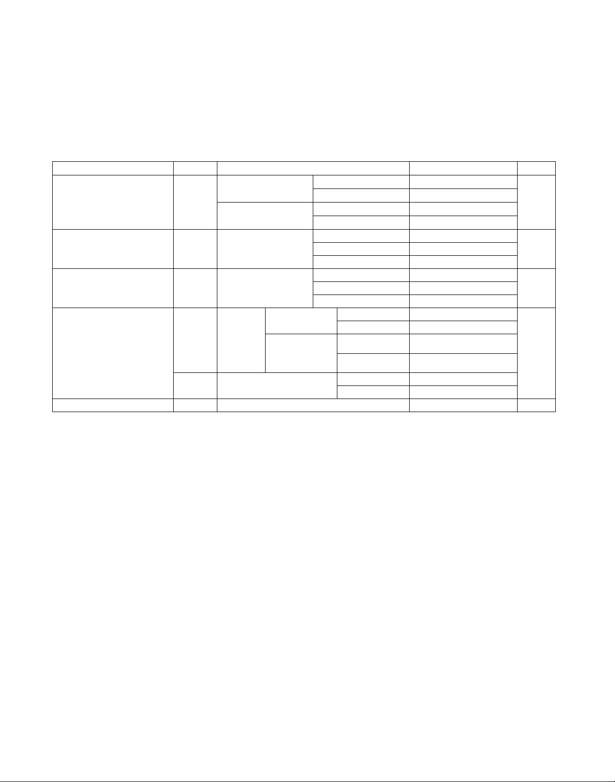
ELECTRICAL CHARACTERISTICS (continued)
(VCC= 2.7V to 5.5V, VEE= 0V, VCM= 0V, TA= -40°C to +85°C, unless otherwise noted. Typical values are at TA= +25°C.) (Note 1)
CONDITIONS UNITSMIN TYP MAXSYMBOLPARAMETER
µs20t
PU
Power-Up Time
nsVCC= 5.0V
80
t
FALL
OUT Fall Time 50
40
300
450
100mV overdrive
100mV overdrive
CL= 15pF
300
t
PD+
Propagation Delay
450
ns
450
t
PD-
300
MAX985/MAX989/
MAX993 only
10mV overdrive
100mV overdrive
MAX985/MAX989/
MAX993 only, CL= 15pF
10mV overdrive
10mV overdrive
CL= 15pF
CL= 50pF
CL= 200pF
MAX986/MAX990/
MAX994 only,
R
PULLUP
= 5.1kΩ
Note 1: All device specifications are 100% production tested at TA= +25°C. Limits over the extended temperature range are guar-
anteed by design.
Note 2: Inferred from the V
OS
test. Both or either inputs can be driven 0.3V beyond either supply rail without output phase reversal.
Note 3: V
OS
is defined as the center of the hysteresis band at the input.
Note 4: I
B
is defined as the average of the two input bias currents (IB-, IB+).
CL= 15pF
CL= 50pF
CL= 200pF
VCC= 5.0V ns
80
t
RISE
OUT Rise Time
(MAX985/MAX989/
MAX993 only)
50
40
VCC= 5V,
I
SOURCE
= 8mA
V
4.6 4.85
V
OH
OUT Output Voltage High
(MAX985/MAX989/
MAX993 only)
TA= +25°C
4.45TA= -40°C to +85°C
VCC= 2.7V,
I
SOURCE
= 3.5mA
2.4 2.55TA= +25°C
2.3TA= -40°C to +85°C
Page 4
MAX985/MAX986/MAX989/
MAX990/MAX993/MAX994
Micropower, Low-Voltage, UCSP/SC70,
Rail-to-Rail I/O Comparators
4
Maxim Integrated
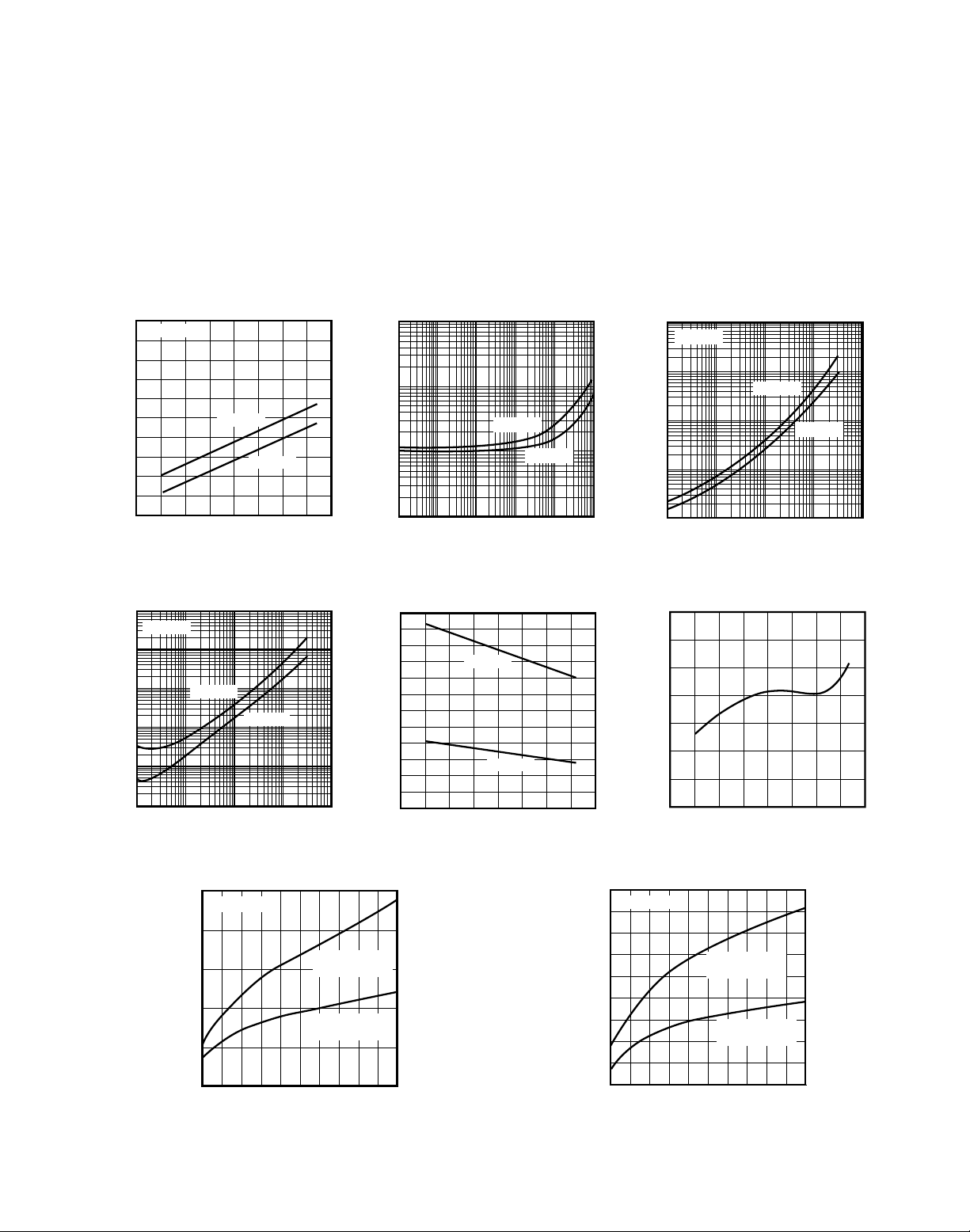
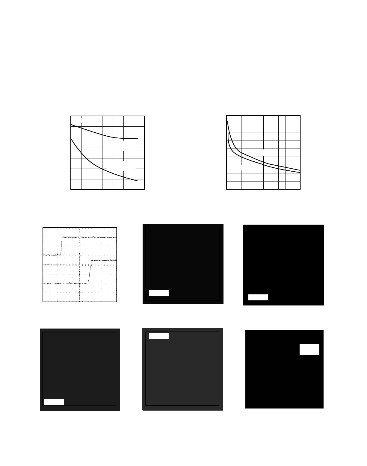
__________________________________________Typical Operating Characteristics
(VCC= 5V, VCM= 0V, TA= +25°C, unless otherwise noted.)
SUPPLY CURRENT
vs. TEMPERATURE
18
V
> V
IN+
17
16
15
14
13
12
11
SUPPLY CURRENT (µA)
10
9
8
-60 100
IN-
VCC = 5.0V
VCC = 2.7V
-40 -20 0 20 40 60 80
TEMPERATURE (°C)
OUTPUT HIGH VOLTAGE
vs. OUTPUT SOURCE CURRENT
10,000
V
> V
IN+
)
OH
1000
- V
CC
100
(mV)
10
1
OUTPUT HIGH VOLTAGE (V
0.1
0.01
IN-
VCC = 2.7V
VCC = 5.0V
0.1
OUTPUT SOURCE CURRENT (mA)
1 10 100
PROPAGATION DELAY
vs. CAPACITIVE LOAD (V
600
VOD = 50mV
550
500
(ns)
PD
t
450
400
350
0
200 1000
TO V
FINAL VALUE
TO V
FINAL VALUE
400
CAPACITIVE LOAD (pF)
1000
MAX985-01
100
10
SUPPLY CURRENT (µA)
1
0.01 0.1 1 10 100 1000
120
110
MAX985-08
100
90
80
70
60
50
40
30
OUTPUT SINK CURRENT (mA)
20
10
0
-60
= 3V)
CC
MAX985-05a
= 50% OF
OUT
= 10% OF
OUT
800600
SUPPLY CURRENT vs.
OUTPUT TRANSITION FREQUENCY
VCC = 5.0V
VCC = 2.7V
OUTPUT TRANSITION FREQUENCY (kHz)
OUTPUT SHORT-CIRCUIT
CURRENT vs. TEMPERATURE
VCC = 5.0V
VCC = 2.7V
-40 -20 0 20 40 60 80
TEMPERATURE (°C)
OUTPUT LOW VOLTAGE
vs. OUTPUT SINK CURRENT
10,000
)
MAX985-02
OL
OUTPUT LOW VOLTAGE (mV) (V
V
< V
IN+
IN-
1000
100
10
1
0.01 0.1 1 10 100
OUTPUT SINK CURRENT (mA)
INPUT OFFSET VOLTAGE
vs. TEMPERATURE
1.1
MAX985-06
0.9
0.7
0.5
0.3
OFFSET VOLTAGE (mV)
0.1
-0.1
-0.3
-60 100
100
-40 -20 0 20 40 60 80
PROPAGATION DELAY
vs. CAPACITIVE LOAD (V
530
VOD = 50mV
510
490
470
450
(ns)
PD
t
430
410
390
370
350
0 200 1000
TO V
FINAL VALUE
TO V
FINAL VALUE
400
CAPACITIVE LOAD (pF)
VCC = 2.7V
TEMPERATURE (°C)
= 5V)
CC
= 50% OF
OUT
= 10% OF
OUT
800600
V
CC
MAX985-04
= 5.0V
MAX985-07
MAX985-05b
Page 5
5
Maxim Integrated
MAX985/MAX986/MAX989/
MAX990/MAX993/MAX994
Micropower, Low-Voltage, UCSP/SC70,
Rail-to-Rail I/O Comparators
/
PROPAGATION DELAY (t
PD-
)
IN+
OUT
MAX985-12
100ns/div
50mV/
div
2V/div
VOD = 50mV
____________________________Typical Operating Characteristics (continued)
(VCC= 5V, VCM= 0V, TA= +25°C, unless otherwise noted.)
OUT
(ns)
PD
t
MAX985/MAX989/MAX993
PROPAGATION DELAY (t
IN+
PROPAGATION DELAY
vs. TEMPERATURE
450
VOD = 50mV
440
430
TO V
= 50% POINT
420
410
400
390
380
-40 100
-20 0 20 40 60 80
TEMPERATURE (°C)
OF FINAL VALUE
TO V
OF FINAL VALUE
)
PD+
MAX985-11
OUT
= 10% POINT
OUT
50mV
div
2V/div
MAX985-09
PROPAGATION DELAY
vs. INPUT OVERDRIVE
900
800
700
600
500
(ns)
PD
t
400
300
200
100
0
0 80 120 160 200
VCC = 2.7V
VCC = 5.0V
40
INPUT OVERDRIVE (mV)
MAX985/MAX989/MAX993
SWITCHING CURRENT, OUT RISING
IN+
OUT
MAX985-10
MAX985-13
50mV/
div
2V/div
VOD = 50mV
SWITCHING CURRENT, OUT FALLING
IN+
OUT
I
CC
VOD = 50mV
100ns/div
100ns/div
MAX985-16
= 50mV
= 0V
1mA/div
I
CC
VOD = 50mV
100ns/div
MAX985-14
IN+
50mV/
div
2V/div
OUT
1mA/div
1MHz RESPONSE
VOD = 50mV
200ns/div
MAX985-15
50mV/
div
2V/div
V
OUT
CC
POWER-UP DELAY
5µs/div
V
IN-
V
IN+
Page 6
MAX985/MAX986/MAX989/
MAX990/MAX993/MAX994
Micropower, Low-Voltage, UCSP/SC70,
Rail-to-Rail I/O Comparators
6
Maxim Integrated
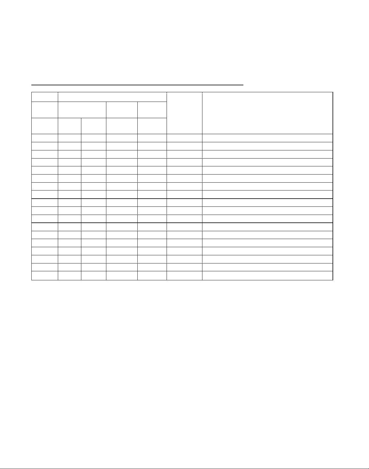
Pin/Bump Description
*
MAX985 only
BUMP PIN
MAX985
UCSP* SO
A2 6 1 — — OUT Comparator Output
A3 7 2 8 4 V
B1 3 3 — — IN+ Comparator Noninverting Input
B2 2 4 — — IN- Comparator Inverting Input
A1 4 5 4 11 V
— — — 1 1 OUTA Comparator A Output
— — — 2 2 INA- Comparator A Inverting Input
— — — 3 3 INA+ Comparator A Noninverting Input
— — — 5 5 INB+ Comparator B Noninverting Input
— — — 6 6 INB- Comparator B Inverting Input
— — — 7 7 OUTB Comparator B Output
— — — — 8 OUTC Comparator C Output
— — — — 9 INC- Comparator C Inverting Input
B3 1, 5, 8 — — — N.C. No Connection. Not internally connected.
MAX985/
MAX986
SOT23/
SC70
MAX989/
MAX990
SO/µMAX/
SOT23
MAX993/
MAX994
SO/
TSSOP
10 INC+ Comparator C Noninverting Input
12 IND+ Comparator D Noninverting Input
13 IND- Comparator D Inverting Input
14 OUTD Comparator D Output
NAME FUNCTION
CC
EE
Positive Supply Voltage
Negative Supply Voltage
Page 7
7
Maxim Integrated
MAX985/MAX986/MAX989/
MAX990/MAX993/MAX994
Micropower, Low-Voltage, UCSP/SC70,
Rail-to-Rail I/O Comparators
_______________Detailed Description
The MAX985/MAX986/MAX989/MAX990/MAX993/
MAX994 are single/dual/quad low-power, low-voltage
comparators. They have an operating supply voltage
range between 2.5V and 5.5V and consume only 11µA.
Their common-mode input voltage range extends 0.25V
beyond each rail. Internal hysteresis ensures clean output switching, even with slow-moving input signals.
Large internal output drivers allow rail-to-rail output
swing with up to 8mA loads.
The output stage employs a unique design that minimizes supply-current surges while switching, virtually
eliminating the supply glitches typical of many other
comparators. The MAX985/MAX989/MAX993 have a
push-pull output structure that sinks as well as sources
current. The MAX986/MAX990/MAX994 have an opendrain output stage that can be pulled beyond VCCto an
absolute maximum of 6V above VEE.
Input Stage Circuitry
The devices’ input common-mode range extends from
-0.25V to (VCC+ 0.25V). These comparators may operate at any differential input voltage within these limits.
Input bias current is typically 1.0pA if the input voltage
is between the supply rails. Comparator inputs are protected from overvoltage by internal body diodes connected to the supply rails. As the input voltage exceeds
the supply rails, these body diodes become forward
biased and begin to conduct. Consequently, bias currents increase exponentially as the input voltage
exceeds the supply rails.
Output Stage Circuitry
These comparators contain a unique output stage
capable of rail-to-rail operation with up to 8mA loads.
Many comparators consume orders of magnitude more
current during switching than during steady-state operation. However, with this family of comparators, the
supply-current change during an output transition is
extremely small. The
Typical Operating Characteristics
graph Supply Current vs. Output Transition Frequency
shows the minimal supply-current increase as the output switching frequency approaches 1MHz. This characteristic eliminates the need for power-supply filter
capacitors to reduce glitches created by comparator
switching currents. Another advantage realized in highspeed, battery-powered applications is a substantial
increase in battery life.
__________Applications Information
Additional Hysteresis
MAX985/MAX989/MAX993
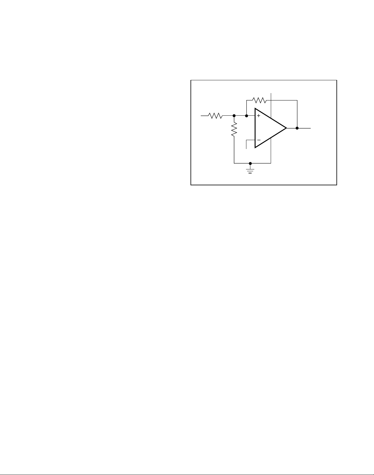
The MAX985/MAX989/MAX993 have ±3mV internal
hysteresis. Additional hysteresis can be generated with
three resistors using positive feedback (Figure 1).
Unfortunately, this method also slows hysteresis
response time. Use the following procedure to calculate resistor values for the MAX985/MAX989/MAX993.
1) Select R3. Leakage current at IN is under 10nA, so
the current through R3 should be at least 1µA to
minimize errors caused by leakage current. The current through R3 at the trip point is (V
REF
- V
OUT
) /
R3. Considering the two possible output states in
solving for R3 yields two formulas: R3 = V
REF
/ 1µA
or R3 = (V
REF
- VCC) / 1µA. Use the smaller of the
two resulting resistor values. For example, if V
REF
=
1.2V and VCC= 5V, then the two R3 resistor values
are 1.2MΩ and 3.8MΩ. Choose a 1.2MΩ standard
value for R3.
2) Choose the hysteresis band required (VHB). For this
example, choose 50mV.
3) Calculate R1 according to the following equation:
R1 = R3 x (V
HB
/ VCC)
For this example, insert the values R1 = 1.2MΩ x
(50mV / 5V) = 12kΩ.
4) Choose the trip point for VINrising (V
THR
; V
THF
is
the trip point for V
IN
falling). This is the threshold
voltage at which the comparator switches its output
from low to high as V
IN
rises above the trip point. For
this example, choose 3V.
Figure 1. Additional Hysteresis (MAX985/MAX989/MAX993)
V
CC
R3
V
R1
IN
R2
V
REF
V
CC
OUT
V
EE
MAX985
MAX989
MAX993
Page 8
MAX985/MAX986/MAX989/
MAX990/MAX993/MAX994
Micropower, Low-Voltage, UCSP/SC70,
Rail-to-Rail I/O Comparators
8
Maxim Integrated
5) Calculate R2 as follows. For this example, choose an
8.2kΩ standard value:
6) Verify trip voltages and hysteresis as follows:
MAX986/MAX990/MAX994
The MAX986/MAX990/MAX994 have ±3mV internal
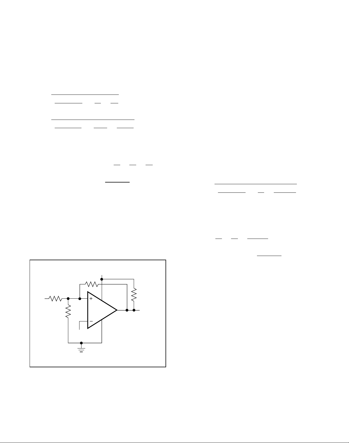
hysteresis. They have open-drain outputs and require
an external pullup resistor (Figure 2). Additional hysteresis can be generated using positive feedback, but
the formulas differ slightly from those of the
MAX985/MAX989/MAX993.
Use the following procedure to calculate resistor
values:
1) Select R3 according to the formulas R3 = V
REF
/
500µA or R3 = (V
REF
- VCC) / 500µA - R4. Use the
smaller of the two resulting resistor values.
2) Choose the hysteresis band required (VHB). For this
example, choose 50mV.
3) Calculate R1 according to the following equation:
R1 = (R3 + R4) x (VHB/ VCC)
4) Choose the trip point for VINrising (V
THR
; V
THF
is
the trip point for VINfalling). This is the threshold
voltage at which the comparator switches its output
from low to high as VINrises above the trip point.
5) Calculate R2 as follows:
6) Verify trip voltages and hysteresis as follows:
Board Layout and Bypassing
Power-supply bypass capacitors are not typically needed, but use 100nF bypass capacitors when supply
impedance is high, when supply leads are long,
or when excessive noise is expected on the supply
lines. Minimize signal trace lengths to reduce stray
capacitance.
Figure 2. Additional Hysteresis (MAX986/MAX990/MAX994)
R2 =
R2 =
⎛
V
THR
⎜
V
⎝
REF
⎛
3.0V
⎜
1.2 x 12k
⎝
1
⎞
1
−−
⎟
1
xR R R
⎠
1
1
3
1
⎞
⎟
ΩΩ Ω
⎠
1
−−
12
kM
22
.
1
803
.
=
k
Ω
V rising: V = V x R1 x
IN THR REF
V falling
IN
Hysteresis V V
⎛
:
=−
VV
THF THR
=−
THR THF
RxV
⎜
⎝
⎛
⎜
⎝
1
1
R1
R
3
1
++
2
RR
⎞
CC
⎟
⎠
⎞
1
⎟
3
⎠
V
CC
R3
R2 =
⎛
V
THR
⎜
V
⎝
REF
1
⎞
1
−−
⎟
1
⎠
1
xR R R R1
34
+
V rising: V = V x R1 x
IN THR REF
V falling
IN
Hysteresis V V
⎛
⎜
R1
⎝
:
VV
=−
1
1
++
2
RRR
=−
THF THR
THR THF
34
⎞
1
⎟
+
⎠
⎛
1
RxV
⎜
⎝
CC
+
34
RR
⎞
⎟
⎠
R1
V
IN
R2
V
REF
V
V
CC
EE
OUT
MAX986
MAX990
MAX994
R4
Page 9
9
Maxim Integrated
MAX985/MAX986/MAX989/
MAX990/MAX993/MAX994
Micropower, Low-Voltage, UCSP/SC70,
Rail-to-Rail I/O Comparators
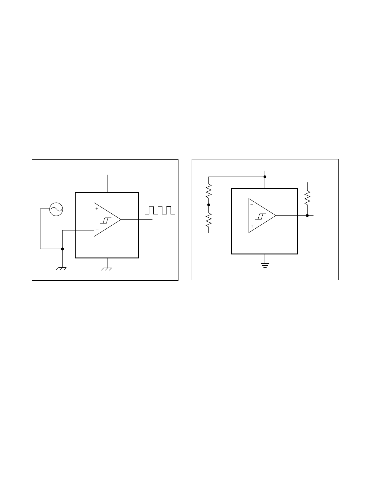
Zero-Crossing Detector
Figure 3 shows a zero-crossing detector application.
The MAX985’s inverting input is connected to ground,
and its noninverting input is connected to a 100mV
P-P
signal source. As the signal at the noninverting input
crosses 0V, the comparator’s output changes state.
Logic-Level Translator
Figure 4 shows an application that converts 5V logic levels to 3V logic levels. The MAX986 is powered by the 5V
supply voltage, and the pullup resistor for the MAX986’s
open-drain output is connected to the 3V supply voltage.
This configuration allows the full 5V logic swing without
creating overvoltage on the 3V logic inputs. For 3V to 5V
logic-level translation, simply connect the 3V supply to
VCCand the 5V supply to the pullup resistor.
Figure 3. Zero-Crossing Detector Figure 4. Logic-Level Translator
V
CC
2
V
100mV
3
IN+
4
IN-
CC
V
EE
MAX985
5
OUT
1
5V (3V)
3V (5V)
100kΩ
4
100kΩ
3
5V (3V) LOGIC IN
IN-
IN+
V
CC
V
EE
2
MAX986
5
OUT
R
PULLUP
3V (5V)
1
LOGIC OUT
Page 10
MAX985/MAX986/MAX989/
MAX990/MAX993/MAX994
Micropower, Low-Voltage, UCSP/SC70,
Rail-to-Rail I/O Comparators
10
Maxim Integrated
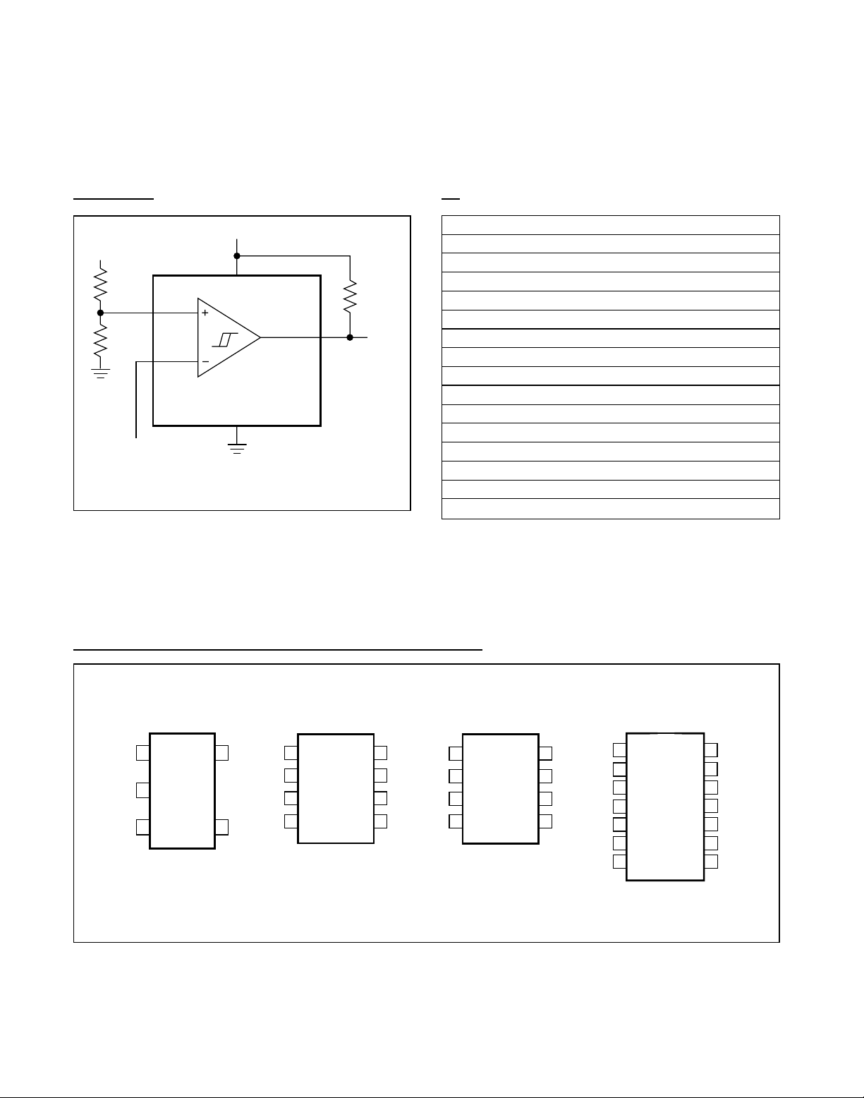
Ordering Information (continued)Typical Application Circuit
Pin Configurations (continued)
Note: All devices are specified over the -40°C to +85°C operating
temperature range.
+
Denotes a lead(Pb)-free/RoHS-compliant package.
T = Tape and reel.
V
CC
V
IN
V
CC
IN+
OUT
IN-
*R
PULLUP
MAX98_
MAX99_
V
EE
V
REF
*MAX986/MAX990/MAX994 ONLY.
THRESHOLD DETECTOR
PART PIN-PACKAGE TOP MARK
MAX985EUK+T 5 SOT23
MAX985ESA+ 8 SO
MAX986EXK+T 5 SC70
MAX986EUK+T 5 SOT23
MAX986ESA+ 8 SO
MAX989EKA+T 8 SOT23
MAX989EUA+T 8 µMAX
MAX989ESA+ 8 SO
MAX990EKA+T 8 SOT23
MAX990EUA+T 8 µMAX
MAX990ESA+ 8 SO
MAX993EUD+ 14 TSSOP
MAX993ESD+ 14 SO
MAX994EUD+ 14 TSSOP
MAX994ESD+ 14 SO
ABYZ
—
ABL
ABZA
—
AADZ
—
—
AAEA
—
—
—
—
—
—
TOP VIEW
OUT
V
CC
IN+
+
1
MAX985
2
MAX986
3
SOT23/SC70
INA-
V
INB-
CC
+
1
2
3
4
5
6
7
MAX993
MAX994
SO/TSSOP
14
OUTD
13
IND-
12
IND+
11
V
EE
INC+
10
9
INC-
OUTCOUTB
8
5
V
EE
IN-
4
N.C.
V
+
1
2
IN-
IN+
EE
MAX985
MAX986
3
4
87N.C.
V
6
OUT
5
N.C.
OUTA
CC
SO
+
1
2
INA-
3
INA+
V
4
EE
SO/µMAX/SOT23
MAX989
MAX990
87V
6
5
CC
OUTB
INB-
INB+
OUTA
INA+
INB+
Page 11
11
Maxim Integrated
MAX985/MAX986/MAX989/
MAX990/MAX993/MAX994
Micropower, Low-Voltage, UCSP/SC70,
Rail-to-Rail I/O Comparators
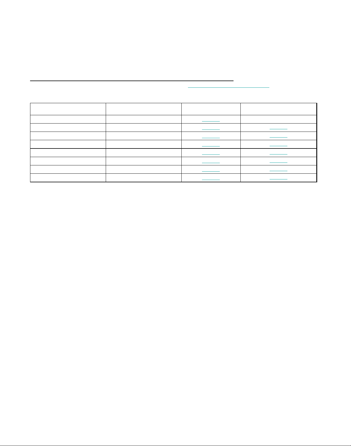
PACKAGE TYPE PACKAGE CODE OUTLINE NO.
LAND
PATTERN NO.
6 UCSP B6+3
21-0097
—
5 SOT23 U5+1
21-0057
90-0174
5 SC70 X5+1
21-0076
90-0188
8 SO S8+2
21-0041
90-0096
8 SOT23 K8+5
21-0078
90-0176
8 µMAX U8+1
21-0036
90-0092
14 SO S14+1
21-0041
90-0112
14 TSSOP U14+1
21-0066
90-0113
Package Information
For the latest package outline information and land patterns (footprints), go to www.maximintegrated.com/packages. Note that a “+”, “#”, or
“-” in the package code indicates RoHS status only. Package drawings may show a different suffix character, but the drawing pertains to the
package regardless of RoHS status.
Page 12
Maxim Integrated cannot assume responsibility for use of any circuitry other than circuitry entirely embodied in a Maxim Integrated product. No circuit patent
licenses are implied. Maxim Integrated reserves the right to change the circuitry and specifications without notice at any time. The parametric values (min and
max limits) shown in the Electrical Characteristics table are guaranteed. Other parametric values quoted in this data sheet are provided for guidance.
12
________________________________Maxim Integrated 160 Rio Robles, San Jose, CA 95134 USA 1-408-601-1000
© 2012 Maxim Integrated Products, Inc. Maxim Integrated and the Maxim Integrated logo are trademarks of Maxim Integrated Products, Inc.
MAX985/MAX986/MAX989/
MAX990/MAX993/MAX994
Micropower, Low-Voltage, UCSP/SC70,
Rail-to-Rail I/O Comparators
Revision History
REVISION
NUMBER
5 4/12
6 8/12 Updated Ordering Information and Figure 3 1, 9
REVISION
DATE
DESCRIPTION
Replaced Figure 3, added lead-free compliant packaging info, updated package
information, updated Absolute Maximum Ratings, rearranged Pin Description table
PAGES
CHANGED
1, 2, 6, 9, 10
 Loading...