

Page 1
19-5519; Rev 0; 9/10
EVALUATION KIT
AVAILABLE
Mono 3.2W Class D Amplifier
General Description
The MAX98304 mono 3.2W Class D amplifier provides
Class AB audio performance with Class D efficiency.
This device offers five selectable gain settings (0dB,
3dB, 6dB, 9dB, and 12dB) set by a single gain-select
input (GAIN).
Active emissions-limiting, edge-rate, and overshoot control circuitry greatly reduces EMI. A filterless spreadspectrum modulation scheme eliminates the need for
output filtering found in traditional Class D devices. These
features reduce application component count.
The IC's 0.95mA at 3.7V (1.2mA at 5V) quiescent current
extends battery life in portable applications.
The IC is available in a 9-bump (1.0mm x 1.0mm) WLP
with 0.3mm pitch that is specified over the extended
-40NC to +85NC temperature range.
Features
S Low Quiescent Current: 0.95mA at 3.7V
S Spread Spectrum and Active Emissions Limiting
S Five Pin-Selectable Gains
S 19µV
S 90dB PSRR
S Click-and-Pop Suppression
S Thermal and Overcurrent Protection
S Low-Current Shutdown Mode
S 1.0mm x 1.0mm, 9-Bump WLP (0.3mm Pitch)
Space-Saving Package
Ultra-Low Noise
RMS
MAX98304
Applications
Notebook and Netbook Computers
Cellular Phones
Tablets
MP3 Players
Portable Audio Players
VoIP Phones
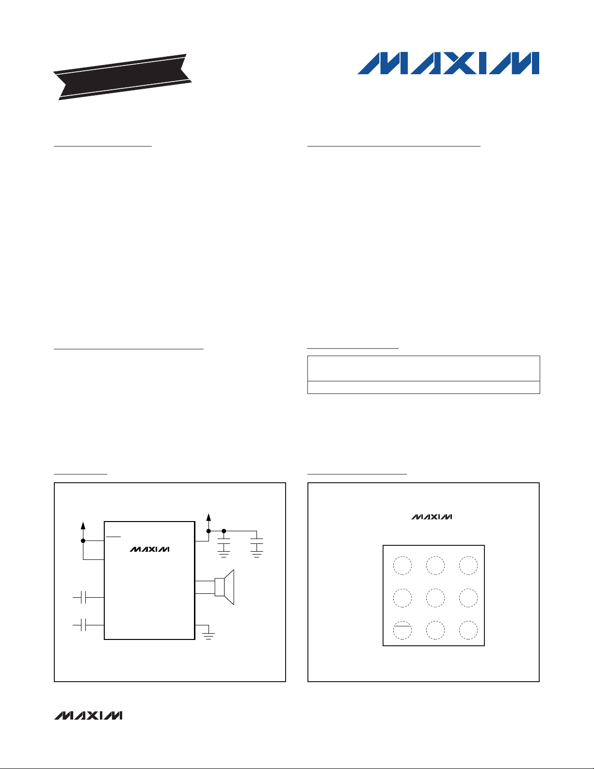
Typical Application Circuit
+2.5V TO +5.5V
0.47µF
0.47µF
SHDN
GAIN
IN+
IN-
MAX98304
+2.5V TO +5.5V
PVDD
OUT+
OUT-
PGND
0.1µF
10µF*
Ordering Information
PART TEMP RANGE
MAX98304EWL+
+Denotes a lead(Pb)-free/RoHS-compliant package.
-40NC to +85NC
PINPACKAGE
9 WLP AIR
TOP
MARK
Bump Configuration
TOP VIEW
BUMP SIDE DOWN
MAX98304
1 2 3
+
OUT-
A
PGND
B
C
SHDN
N.C.
IN- IN+
PVDDOUT+
GAIN
*SYSTEM BULK CAPACITANCE
(1mm x 1mm x 0.64mm
_______________________________________________________________ Maxim Integrated Products 1
WLP
0.3mm PITCH)
For pricing, delivery, and ordering information, please contact Maxim Direct at 1-888-629-4642,
or visit Maxim’s website at www.maxim-ic.com.
Page 2
Mono 3.2W Class D Amplifier
ABSOLUTE MAXIMUM RATINGS
PVDD, IN+, IN-, SHDN, GAIN to PGND ..................-0.3V to +6V
All Other Pins to PGND .........................-0.3V to (V
Continuous Current Into/Out of PVDD, PGND, OUT_ ... Q750mA
Continuous Input Current (all other pins) ........................ Q20mA
Duration of Short Circuit Between
OUT_ and PVDD, PGND .......................................Continuous
OUT+ and OUT- ....................................................Continuous
Stresses beyond those listed under “Absolute Maximum Ratings” may cause permanent damage to the device. These are stress ratings only, and functional
MAX98304
operation of the device at these or any other conditions beyond those indicated in the operational sections of the specifications is not implied. Exposure to absolute
maximum rating conditions for extended periods may affect device reliability.
PVDD
+ 0.3V)
ELECTRICAL CHARACTERISTICS
(V
bandwidth 20Hz to 22kHz, TA = T
= V
PVDD
Supply Voltage Range PVDD Inferred from PSRR test 2.5 5.5 V
Undervoltage Lockout UVLO PVDD falling 1.5 1.8 2.2 V
Quiescent Supply Current I
Shutdown Supply Current I
Turn-On Time t
Bias Voltage V
Input Resistance R
Voltage Gain A
Output Offset Voltage V
Click and Pop K
Common-Mode Rejection Ratio CMRR fIN = 1kHz, input referred 80 dB
= 5.0V, V
SHDN
PARAMETER SYMBOL CONDITIONS MIN TYP MAX UNITS
= 0V, AV = 12dB (GAIN = PGND), RL = J, RL connected between OUT+ to OUT-, AC measurement
PGND
MIN
to T
, unless otherwise noted. Typical values are at TA = +25NC.) (Notes 1, 2)
MAX
TA = +25NC
DD
V
= 3.7V 0.95
PVDD
V
SHDN
ON
BIAS
IN
V
OS
CP
= 0V, TA = +25NC
SHDN
TA = +25°C,
single-ended
Connect GAIN to PGND 11.5 12 12.5
Connect GAIN to PGND
through 100kI ±5%
Connect GAIN to PVDD 5.5 6 6.5
Connect GAIN to PVDD
through 100kI ±5%
GAIN unconnected -0.5 0 +0.5
TA = +25°C (Note 3)
Peak voltage,
A-weighted, 32
samples per second,
RL = 8I (Notes 3, 4)
Continuous Power Dissipation (TA = +70NC) for Multilayer Board
9-Bump WLP (derate 10.6mW/NC) ..............................848mW
Junction Temperature .....................................................+150NC
Operating Temperature Range .......................... -40NC to +85NC
Storage Temperature Range ............................ -65NC to +150NC
Soldering Temperature (reflow) ......................................+260NC
1.2 1.8
< 0.1 10
3.4 10 ms
V
PVDD
/2
AV = 12dB 45 70
AV = 9dB 64 100
AV = 6dB 90 140
AV = 3dB 128 200
AV = 0dB 180 280
8.5 9 9.5
2.5 3 3.5
Q1 Q4.5
Into shutdown -74
Out of shutdown -60
mA
FA
V
kI
dB
mV
dBV
2 ______________________________________________________________________________________
Page 3
Mono 3.2W Class D Amplifier
ELECTRICAL CHARACTERISTICS (continued)
(V
bandwidth 20Hz to 22kHz, TA = T
Note 1: This device is 100% production tested at +25NC. All temperature limits are guaranteed by design.
Note 2: Testing performed with a resistive load in series with an inductor to simulate an actual speaker load. For RL = 4I,
Note 3: Amplifier inputs AC-coupled to ground.
Note 4: Mode transitions controlled by SHDN.
PVDD
= V
SHDN
= 5.0V, V
= 0V, AV = 12dB (GAIN = PGND), RL = J, RL connected between OUT+ to OUT-, AC measurement
PGND
MIN
to T
, unless otherwise noted. Typical values are at TA = +25NC.) (Notes 1, 2)
MAX
PARAMETER SYMBOL CONDITIONS MIN TYP MAX UNITS
72 90
Power-Supply Rejection Ratio
(Note 3)
PSRR
V
= 2.5V to 5.5V, TA = +25NC
PVDD
V
= 200mV
RIPPLE
P-P
f = 217Hz 80
f = 1kHz 84
f = 20kHz 84
V
= 5.0V 3.2
PVDD
V
= 4.2V 2.2
PVDD
V
= 3.7V 1.7
PVDD
V
= 5.0V 2.6
PVDD
V
= 4.2V 1.8
PVDD
V
= 3.7V 1.4
PVDD
V
= 5.0V 1.8
PVDD
V
= 4.2V 1.2
PVDD
V
= 3.7V 0.96
PVDD
V
= 5.0V 1.4
PVDD
V
= 4.2V 1
PVDD
V
= 3.7V 0.8
PVDD
RL = 4I
P
= 1W
OUT
RL = 8I
P
= 0.7W
OUT
0.03 0.1
0.03
300 kHz
±12.5
93 %
Output Power P
Total Harmonic Distortion
Plus Noise
THD+N fIN = 1kHz
Oscillator Frequency f
Spread-Spectrum Bandwidth
Efficiency
OUT
OSC
E P
THD+N = 10%,
f = 1kHz,
RL = 4I + 33FH
THD+N = 1%,
f = 1kHz,
RL = 4I + 33FH
THD+N = 10%,
f = 1kHz,
RL = 8I + 68FH
THD+N = 1%,
f = 1kHz,
RL = 8I + 68FH
= 1.75W, RL = 8I
OUT
AV = 12dB 31
AV = 9dB 26
Noise V
A-weighted (Note 3)
N
AV = 6dB 23
AV = 3dB 21
AV = 0dB 19
Output Current Limit I
LIM
2.8 A
Thermal Shutdown Level 155
Thermal Shutdown Hysteresis 15
DIGITAL INPUT (SHDN)
Input-Voltage High V
Input-Voltage Low V
Input Leakage Current
V
INH
INL
= 2.5V to 5.5V 1.4 V
PVDD
V
= 2.5V to 5.5V 0.4 V
PVDD
TA = +25NC Q1 FA
L = 33FH. For RL = 8I, L = 68FH.
FV
MAX98304
dB
W
%
kHz
RMS
NC
NC
_______________________________________________________________________________________ 3
Page 4
Mono 3.2W Class D Amplifier
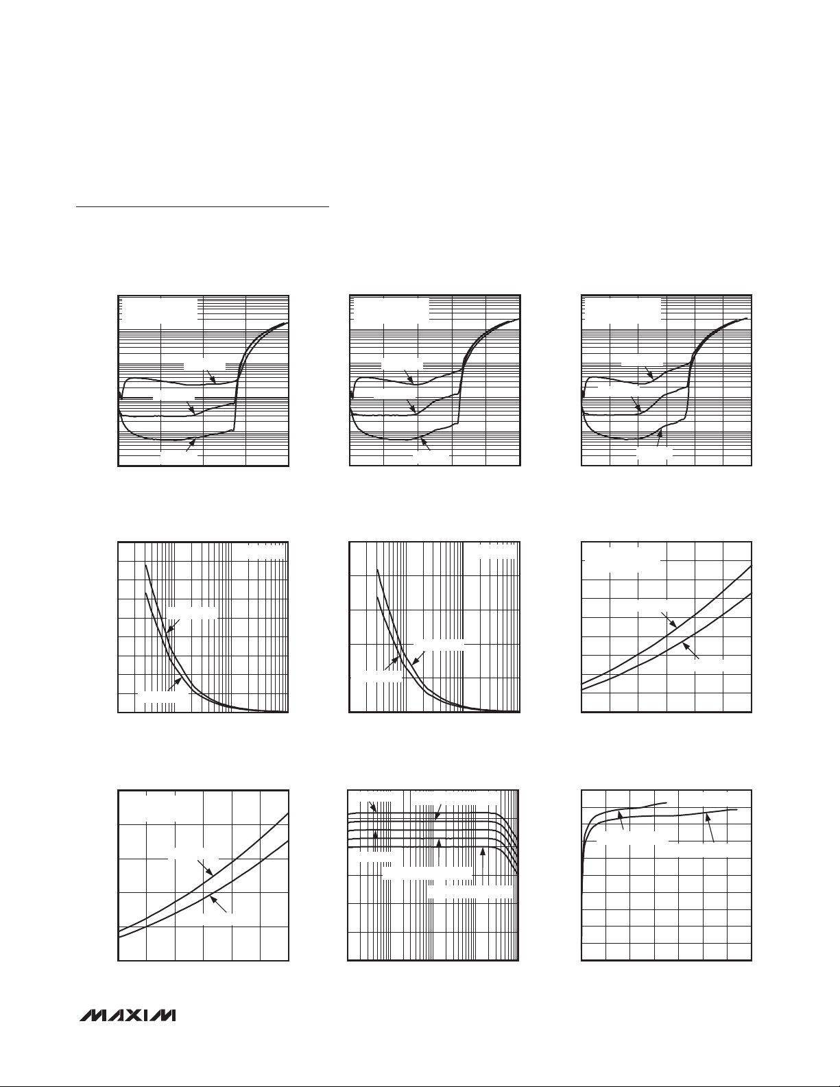
Typical Operating Characteristics
(V
= V
PVDD
to 22kHz, TA = +25NC, unless otherwise noted.)
SHDN
= 5.0V, V
= 0V, AV = 6dB, RL = J, RL connected between OUT+ to OUT-, AC measurement bandwidth 20Hz
PGND
TOTAL HARMONIC DISTORTION PLUS
NOISE vs. FREQUENCY
10
V
= 5V
PVDD
Z
= 4I + 33µH
LOAD
MAX98304
1
P
= 2W
OUT
0.1
THD+N (%)
0.01
0.001
P
= 1.5W
OUT
10 100k
FREQUENCY (Hz)
TOTAL HARMONIC DISTORTION PLUS
NOISE vs. FREQUENCY
10
V
= 5V
PVDD
Z
= 8I + 68µH
LOAD
1
0.1
THD+N (%)
0.01
P
= 1.2W
OUT
P
OUT
= 0.2W
TOTAL HARMONIC DISTORTION PLUS
NOISE vs. FREQUENCY
10
V
= 4.2V
PVDD
Z
= 4I + 33µH
MAX98304 toc01
THD+N (%)
10k1k100
LOAD
1
0.1
0.01
P
OUT
0.001
10 100k
FREQUENCY (Hz)
P
= 0.5W
10k1k100
OUT
= 1W
MAX98304 toc02
TOTAL HARMONIC DISTORTION PLUS
NOISE vs. FREQUENCY
10
V
= 4.2V
PVDD
Z
= 8I + 68µH
0.01
LOAD
1
0.1
P
= 0.6W
OUT
MAX98304 toc05
MAX98304 toc04
THD+N (%)
TOTAL HARMONIC DISTORTION PLUS
NOISE vs. FREQUENCY
10
V
= 3.7V
PVDD
Z
= 4I + 33µH
LOAD
1
0.1
THD+N (%)
0.01
0.001
P
= 0.8W
OUT
P
= 0.2W
OUT
10 100k
FREQUENCY (Hz)
TOTAL HARMONIC DISTORTION PLUS
NOISE vs. FREQUENCY
10
V
= 3.7V
PVDD
Z
= 8I + 68µH
LOAD
1
P
= 0.2W
OUT
0.1
THD+N (%)
0.01
MAX98304 toc03
10k1k100
= 0.4W
MAX98304 toc06
P
OUT
P
= 0.3W
0.001
10 100k
FREQUENCY (Hz)
TOTAL HARMONIC DISTORTION PLUS
NOISE vs. OUTPUT POWER
100
V
= 5V
PVDD
Z
= 4I + 33µH
LOAD
10
1
THD+N (%)
0.1
0.01
0.001
0 4.0
f = 6000Hz
f = 1000Hz
f = 100Hz
OUTPUT POWER (W)
10k1k100
0.001
10 100k
TOTAL HARMONIC DISTORTION PLUS
100
V
PVDD
Z
MAX98304 toc07
THD+N (%)
3.53.02.52.01.51.00.5
LOAD
10
1
0.1
0.01
0.001
0 2.5
OUT
10k1k100
FREQUENCY (Hz)
NOISE vs. OUTPUT POWER
= 4.2V
= 4I + 33µH
f = 6000Hz
f = 1000Hz
f = 100Hz
OUTPUT POWER (W)
0.001
10 100k
FREQUENCY (Hz)
TOTAL HARMONIC DISTORTION PLUS
TOTAL HARMONIC DISTORTION PLUS
NOISE vs. OUTPUT POWER
100
MAX98304 toc08
10
THD+N (%)
0.1
0.01
2.01.51.00.5
0.001
NOISE vs. OUTPUT POWER
V
= 3.7V
PVDD
Z
= 4I + 33µH
LOAD
1
f = 6000Hz
f = 1000Hz
OUTPUT POWER (W)
f = 100Hz
4 ______________________________________________________________________________________
10k1k100
MAX98304 toc09
1.51.00.50
2.0
Page 5
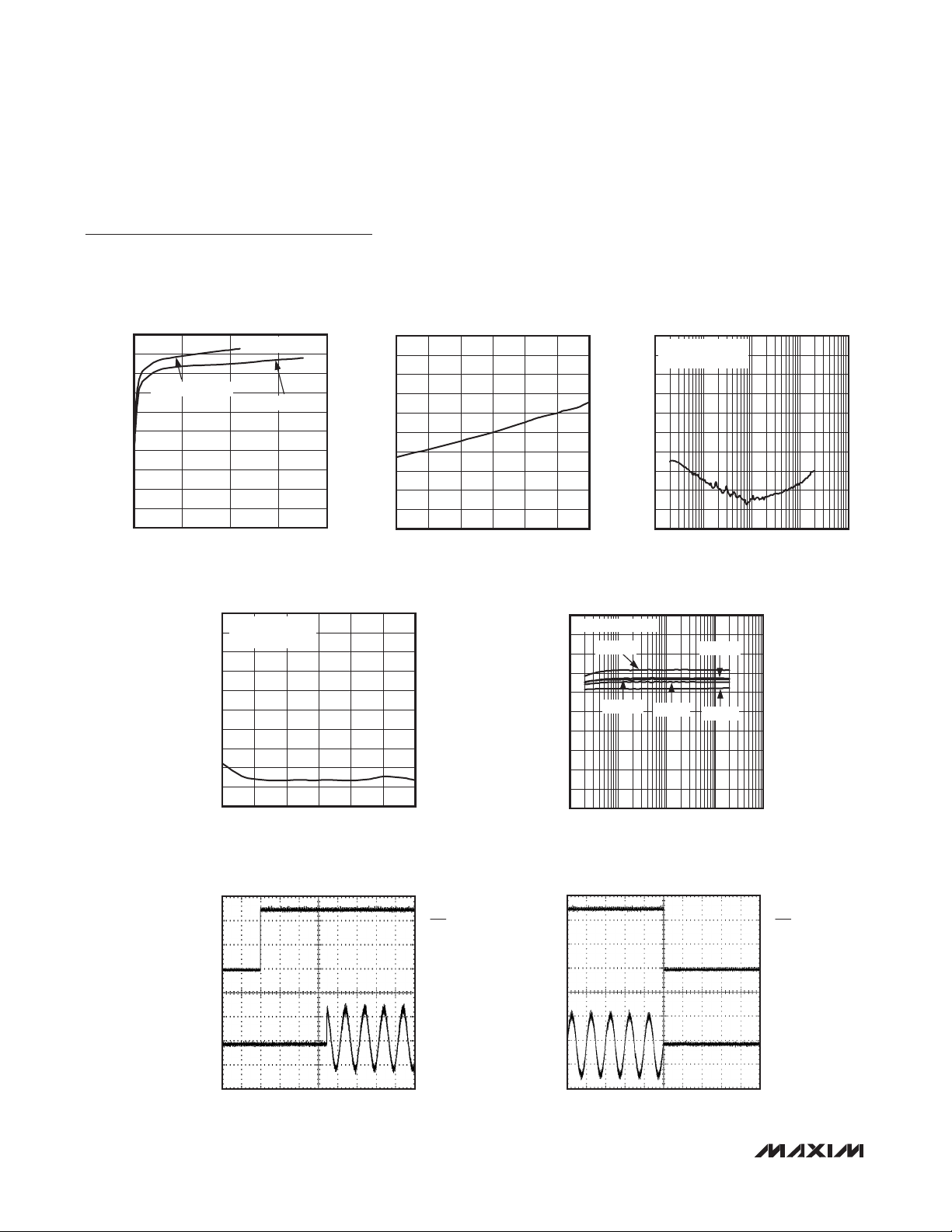
Mono 3.2W Class D Amplifier
AMPLITUDE (dB)
Typical Operating Characteristics (continued)
(V
= V
PVDD
to 22kHz, TA = +25NC, unless otherwise noted.)
SHDN
= 5.0V, V
= 0V, AV = 6dB, RL = J, RL connected between OUT+ to OUT-, AC measurement bandwidth 20Hz
PGND
MAX98304
TOTAL HARMONIC DISTORTION PLUS
TOTAL HARMONIC DISTORTION PLUS
NOISE vs. OUTPUT POWER
100
10
THD+N (%)
0.1
0.01
0.001
NOISE vs. OUTPUT POWER
V
= 5V
PVDD
Z
= 8I + 68µH
LOAD
1
f = 1000Hz
f = 100Hz
OUTPUT POWER (W)
f = 6000Hz
OUTPUT POWER vs. LOAD RESISTANCE
4.5
4.0
3.5
3.0
2.5
2.0
1.5
OUTPUT POWER (W)
1.0
0.5
0
1 1000
THD+N = 10%
THD+N = 1%
R
LOAD
10010
(I)
V
1.51.00.50
PVDD
= 5.0V
MAX98304 toc10
2.0
MAX98304 toc13
TOTAL HARMONIC DISTORTION PLUS
NOISE vs. OUTPUT POWER
100
V
= 4.2V
PVDD
Z
= 8I + 68µH
LOAD
10
1
THD+N (%)
0.1
0.01
0.001
f = 6000Hz
f = 1000Hz
f = 100Hz
0 1.5
OUTPUT POWER (W)
OUTPUT POWER vs. LOAD RESISTANCE
2.5
2.0
1.5
1.0
OUTPUT POWER (W)
THD+N = 1%
0.5
0
1 1000
THD+N = 10%
R
(I)
LOAD
10010
V
PVDD
1.20.90.60.3
= 3.7V
100
MAX98304 toc11
THD+N (%)
0.01
0.001
MAX98304 toc14
OUTPUT POWER (W)
TOTAL HARMONIC DISTORTION PLUS
NOISE vs. OUTPUT POWER
V
= 3.7V
PVDD
Z
= 8I + 68µH
LOAD
10
1
0.1
0 1.2
f = 6000Hz
f = 1000Hz
f = 100Hz
1.00.80.60.40.2
OUTPUT POWER (W)
OUTPUT POWER vs. SUPPLY VOLTAGE
4.5
f = 1kHz
4.0
Z
= 4I + 33µH
LOAD
3.5
3.0
2.5
2.0
1.5
1.0
0.5
0
2.5 5.5
THD+N = 10%
THD+N = 1%
5.04.54.03.53.0
SUPPLY VOLTAGE (V)
MAX98304 toc12
MAX98304 toc15
OUTPUT POWER vs. SUPPLY VOLTAGE
2.5
f = 1kHz
Z
= 8I + 68µH
LOAD
2.0
1.5
1.0
OUTPUT POWER (W)
0.5
0
2.5 5.5
THD+N = 10%
THD+N = 1%
SUPPLY VOLTAGE (V)
_______________________________________________________________________________________ 5
GAIN vs. FREQUENCY
20
GAIN = PGND
10
MAX98304 toc16
0
GAIN = PVDD
-10
-20
-30
5.04.54.03.53.0
-40
GAIN = 100kI TO PGND
GAIN = 100kI TO PVDD
GAIN = UNCONNECTED
1k
FREQUENCY (Hz)
MAX98304 toc17
EFFICIENCY (%)
100k
10k10010
EFFICIENCY vs. OUTPUT POWER
100
90
80
Z
= 8I + 68µH
LOAD
70
60
50
40
30
20
10
0
0 3.5
OUTPUT POWER (W)
Z
LOAD
V
PVDD
= 4I + 33µH
= 5.0V
MAX98304 toc18
3.02.51.5 2.01.00.5
Page 6
Mono 3.2W Class D Amplifier
FREQUENCY (Hz)
Typical Operating Characteristics (continued)
(V
= V
PVDD
to 22kHz, TA = +25NC, unless otherwise noted.)
SHDN
= 5.0V, V
= 0V, AV = 6dB, RL = J, RL connected between OUT+ to OUT-, AC measurement bandwidth 20Hz
PGND
EFFICIENCY vs. OUTPUT POWER
100
90
MAX98304
80
Z
= 8I + 68µH
LOAD
70
60
50
40
EFFICIENCY (%)
30
20
10
0
0 2.0
OUTPUT POWER (W)
0
-10
-20
-30
-40
-50
PSRR (dB)
-60
-70
-80
-90
-100
2.5 5.5
V
= 3.7V
PVDD
MAX98304 toc19
Z
= 4I + 33µH
LOAD
1.51.00.5
POWER-SUPPLY REJECTION
RATIO vs. SUPPLY VOLTAGE
f = 1kHz
V
= 200mV
RIPPLE
P-P
SUPPLY VOLTAGE (V)
SUPPLY CURRENT
vs. SUPPLY VOLTAGE
2.0
1.8
1.6
1.4
1.2
1.0
0.8
0.6
SUPPLY CURRENT (mA)
0.4
0.2
0
2.5 5.5
SUPPLY VOLTAGE (V)
MAX98304 toc22
5.04.54.03.53.0
0
-10
-20
MAX98304 toc20
-30
-40
-50
PSRR (dB)
-60
-70
-80
-90
5.04.54.03.53.0
-100
10 100k
COMMON-MODE REJECTION RATIO
vs. FREQUENCY
100
Z
= 8I + 68µH
LOAD
90
80
70
60
50
CMRR (dB)
40
30
20
10
AV = 9dB
AV = 12dB
0
POWER-SUPPLY REJECTION
RATIO vs. FREQUENCY
V
= 200mV
RIPPLE
Z
LOAD
AV = 3dB
= 8I + 68µH
FREQUENCY (Hz)
AV = 6dB
AV = 0dB
10k1k10010 100k
P-P
MAX98304 toc21
10k1k100
MAX98304 toc23
STARTUP RESPONSE
1ms/div
MAX98304 toc24
V
SHDN
2V/div
I
SPEAKER
100mA/div
SHUTDOWN RESPONSE
1ms/div
MAX98304 toc25
6 ______________________________________________________________________________________
V
SHDN
2V/div
I
SPEAKER
100mA/div
Page 7
Mono 3.2W Class D Amplifier
WLP
(1mm x 1mm x 0.64mm
0.3mm PITCH)
TOP VIEW
BUMP SIDE DOWN
MAX98304
+
OUT-
PGND
SHDN
IN- IN+
N.C.
GAIN
PVDDOUT+
1 2 3
B
C
A
Typical Operating Characteristics (continued)
(V
= V
PVDD
to 22kHz, TA = +25NC, unless otherwise noted.)
SHDN
= 5.0V, V
= 0V, AV = 6dB, RL = J, RL connected between OUT+ to OUT-, AC measurement bandwidth 20Hz
PGND
MAX98304
20
WIDEBAND vs. FREQUENCY
0
-20
-40
-60
OUTPUT MAGNITUDE (dBV)
-80
-100
FREQUENCY (MHz)
RBW = 100Hz
1010.1 100
MAX98304 toc26
0
-20
-40
-60
-80
-100
OUTPUT MAGNITUDE (dBV)
-120
-140
IN-BAND vs. FREQUENCY
f = 1kHz
V
= -60dBV
OUT
10 100k
FREQUENCY (Hz)
10k1k100
MAX98304 toc27
Bump Configuration
TOP VIEW
BUMP SIDE DOWN
A
B
+
MAX98304
1 2 3
OUT-
PGND
N.C.
PVDDOUT+
GAIN
C
SHDN
(1mm x 1mm x 0.64mm
IN- IN+
WLP
0.3mm PITCH)
Bump Description
BUMP NAME FUNCTION
A1 OUT- Negative Speaker Output
A2 OUT+ Positive Speaker Output
A3 PVDD
B1 PGND Ground
B2 N.C. No Connection. Can be left unconnected, or connected to PGND.
B3 GAIN Gain Select. See Table 1 for GAIN settings.
C1
SHDN Active-Low Shutdown Input. Drive SHDN low to place the device in shutdown.
C2 IN- Inverting Audio Input
C3 IN+ Noninverting Audio Input
_______________________________________________________________________________________ 7
Power Supply. Bypass PVDD to PGND with 0.1FF || 10FF.
Page 8

Mono 3.2W Class D Amplifier
Detailed Description
The MAX98304 features low quiescent current, a lowpower shutdown mode, comprehensive click-and-pop
suppression, and excellent RF immunity.
The device offers Class AB audio performance with
Class D efficiency in a minimal board-space solution.
The Class D amplifier features spread-spectrum modulation, edge-rate, and overshoot control circuitry that offers
MAX98304
significant improvements to switch-mode amplifier radiated emissions.
The amplifier features click-and-pop suppression that
reduces audible transients on startup and shutdown.
The amplifier includes thermal overload and short-circuit
protection.
Class D Speaker Amplifier
The filterless Class D amplifier offers much higher efficiency than Class AB amplifiers. The high efficiency of
a Class D amplifier is due to the switching operation of
the output stage transistors. Any power loss associated
with the Class D output stage is mostly due to the I2R
loss of the MOSFET on-resistance and quiescent current
overhead.
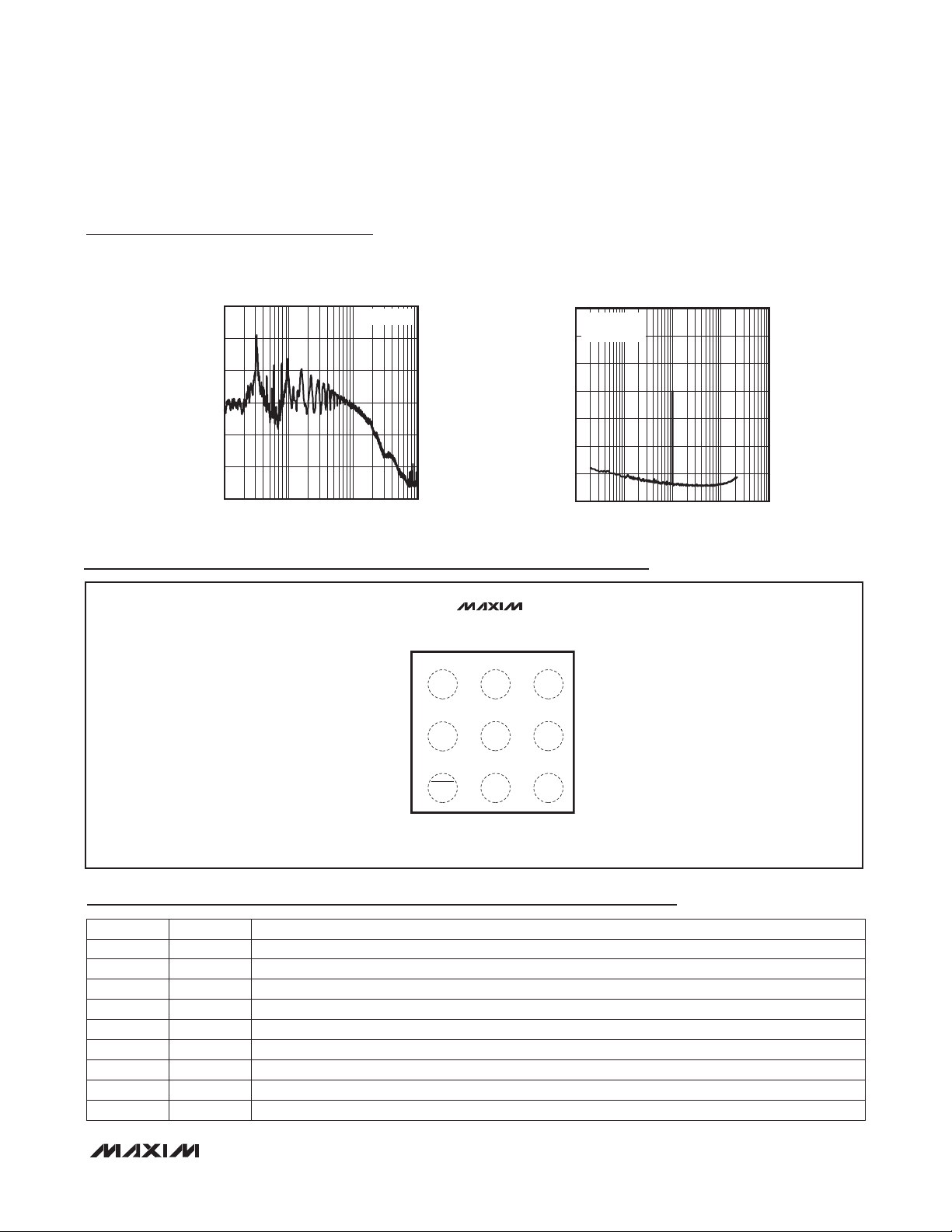
Ultra-Low EMI Filterless Output Stage
Traditional Class D amplifiers require the use of external
LC filters, or shielding, to meet EN55022B electromagnetic-interference (EMI) regulation standards. Maxim’s
patented active emissions-limiting edge-rate control
circuitry and spread-spectrum modulation reduces EMI
emissions, while maintaining up to 93% efficiency.
Maxim’s patented spread-spectrum modulation mode
flattens wideband spectral components, while proprietary techniques ensure that the cycle-to-cycle variation of the switching period does not degrade audio
reproduction or efficiency. The IC’s spread-spectrum
modulator randomly varies the switching frequency by
Q12.5kHz around the center frequency (300kHz). Above
10MHz, the wideband spectrum looks like noise for EMI
purposes (Figure 1).
Speaker Current Limit
If the output current of the speaker amplifier exceeds the
current limit (2.8A typ), the IC disables the outputs for
approximately 100Fs. At the end of 100Fs, the outputs
are reenabled. If the fault condition still exists, the IC
continues to disable and reenable the outputs until the
fault condition is removed.
Selectable Gain
The IC offers five programmable gain selections through
a single gain input (GAIN).
Table 1. Gain Control Configuration
GAIN PIN MAXIMUM GAIN (dB)
Connect to PGND 12
Connect to PGND through
100kW ±5% resistor
Connect to PVDD 6
Connect to PVDD through
100kW ±5% resistor
Unconnected 0
9
3
90
70
50
EN55022B LIMIT
30
EMISSIONS LEVEL (dBµV/m)
10
-10
Figure 1. EMI with 60cm of Speaker Cable and No Output Filtering
8 ______________________________________________________________________________________
HORIZONTAL
VERTICAL
0 100 200 300 400 500 600 700 800 900 1000
FREQUENCY (MHz)
Page 9
Mono 3.2W Class D Amplifier
Shutdown
The IC features a low-power shutdown mode, drawing
less than 0.1FA (typ) of supply current. Drive SHDN low
to put the IC into shutdown.
Click-and-Pop Suppression
The IC speaker amplifier features Maxim’s comprehensive click-and-pop suppression. During startup, the
click-and-pop suppression circuitry reduces any audible
transient sources internal to the device. When entering
shutdown, the differential speaker outputs ramp down to
PGND quickly and simultaneously.
Applications Information
Filterless Class D Operation
Traditional Class D amplifiers require an output filter.
The filter adds cost, size, and decreases efficiency
and THD+N performance. The IC’s filterless modulation
scheme does not require an output filter.
Because the switching frequency of the IC is well
beyond the bandwidth of most speakers, voice coil
movement due to the switching frequency is very small.
Use a speaker with a series inductance > 10FH. Typical
8I speakers exhibit series inductances in the 20FH to
100FH range.
Component Selection
Power-Supply Input (PVDD)
PVDD powers the speaker amplifier. PVDD ranges
from 2.5V to 5.5V. Bypass PVDD with a 0.1FF and 10FF
capacitor to PGND. Apply additional bulk capacitance
at the device if long input traces between PVDD and the
power source are used.
Input Filtering
The input-coupling capacitor (CIN), in conjunction with the
amplifier’s internal input resistance (RIN), forms a highpass filter that removes the DC bias from the incoming
signal. These capacitors allow the amplifier to bias the
signal to an optimum DC level.
Assuming zero source impedance CIN is:
Layout and Grounding
MAX98304
Proper layout and grounding are essential for optimum
performance. Good grounding improves audio performance and prevents switching noise from coupling into
the audio signal.
Use wide, low-resistance output traces. As the load
impedance decreases, the current drawn from the
device increases. At higher current, the resistance of the
output traces decreases the power delivered to the load.
For example, if 2W is delivered from the device output
to a 4I load through 100mI of total speaker trace,
1.904W is being delivered to the speaker. If power is
delivered through 10mI of total speaker trace, 1.99W
is being delivered to the speaker. Wide output, supply,
and ground traces also improve the power dissipation of
the device.
The IC is inherently designed for excellent RF immunity.
For best performance, add ground fills around all signal
traces on top or bottom PCB planes.
WLP Applications Information
For the latest application details on WLP construction,
dimensions, tape carrier information, PCB techniques,
bump-pad layout, and recommended reflow temperature profile, as well as the latest information on reliability
testing results, refer to Application Note 1891: Wafer-
level packaging (WLP) and its applications. Figure 2
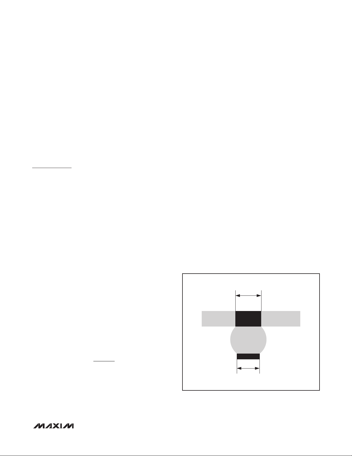
shows the dimensions of the WLP balls used on the IC.
0.18mm
2 R
π ×
C [ F]
= F
IN
where f
input resistance shown in the Electrical Characteristics
table. Use capacitors with adequately low voltage-coefficient for best low-frequency THD performance.
is the -3dB corner frequency and RIN is the
-3dB
_______________________________________________________________________________________ 9
f
−
3dB
IN
0.18mm
Figure 2. MAX98304 WLP Ball Dimensions
Page 10

Mono 3.2W Class D Amplifier
Functional Diagram
2.5V TO 5.5V
MAX98304
0.47µF
0.47µF
SHDN
C1
B3GAIN
C3IN+
C2IN-
MAX98304
0.1µF
UVLO/POWER
MANAGEMENT
PVDD
A3
10µF*
CLICK-AND-POP
CLASS D
MODULATOR
B1
PGND
SUPPRESSION
LOW-EMI
DRIVER
LOW-EMI
DRIVER
PVDD
A1A2OUT-
PGND
PVDD
OUT+
PGND
*SYSTEM BULK CAPACITANCE
Chip Information
PROCESS: CMOS
10 _____________________________________________________________________________________
Page 11
Mono 3.2W Class D Amplifier
Package Information
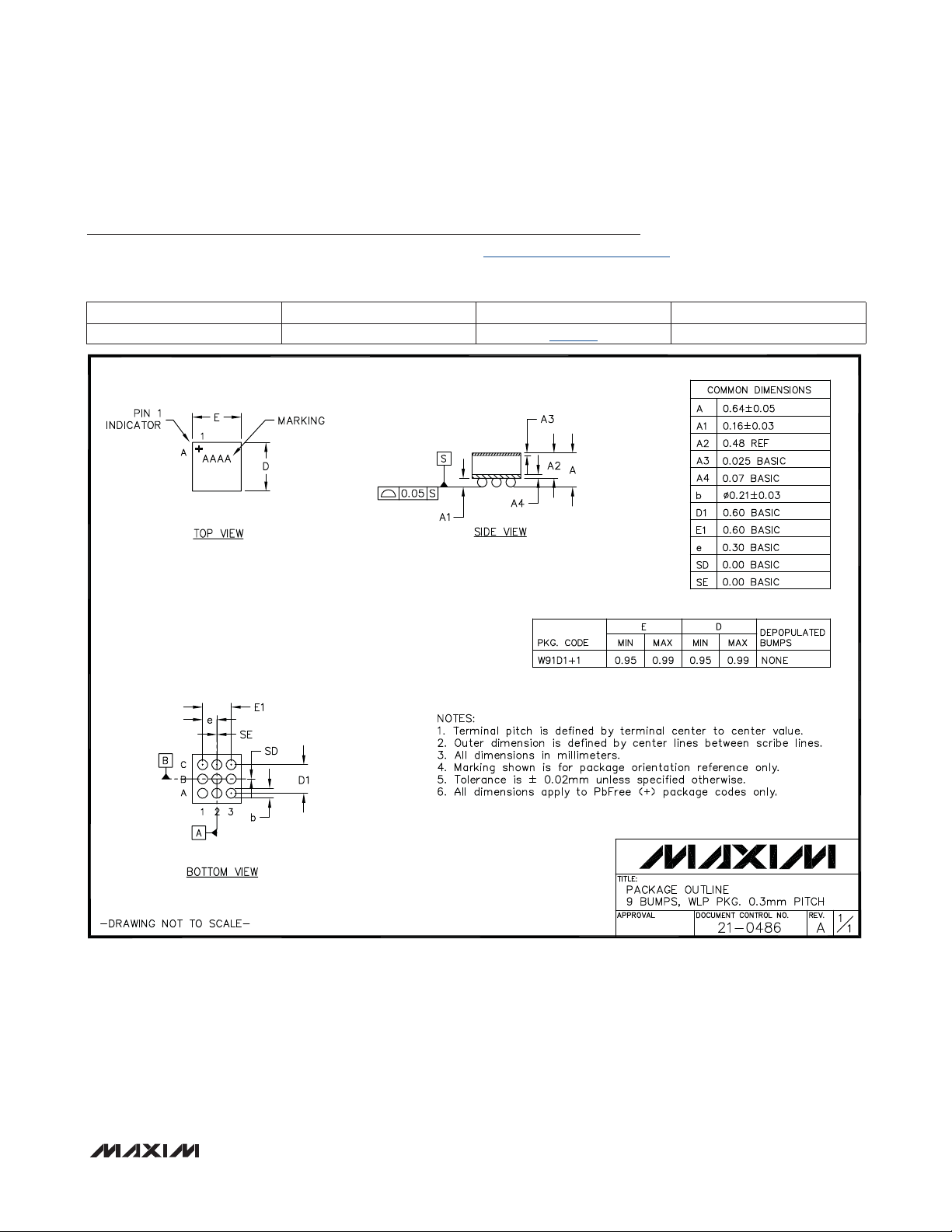
For the latest package outline information and land patterns, go to www.maxim-ic.com/packages. Note that a “+”, “#”, or “-” in the
package code indicates RoHS status only. Package drawings may show a different suffix character, but the drawing pertains to the
package regardless of RoHS status.
PACKAGE TYPE PACKAGE CODE OUTLINE NO. LAND PATTERN NO.
9 WLP W91D1+1
21-0486
—
MAX98304
______________________________________________________________________________________ 11
Page 12
Mono 3.2W Class D Amplifier
Revision History
REVISION
NUMBER
0 9/10 Initial release —
REVISION
DATE
MAX98304
DESCRIPTION
PAGES
CHANGED
Maxim cannot assume responsibility for use of any circuitry other than circuitry entirely embodied in a Maxim product. No circuit patent licenses are implied.
Maxim reserves the right to change the circuitry and specifications without notice at any time.
12 Maxim Integrated Products, 120 San Gabriel Drive, Sunnyvale, CA 94086 408-737-7600
©
2010 Maxim Integrated Products Maxim is a registered trademark of Maxim Integrated Products, Inc.
 Loading...