

Page 1
_______________General Description
The MAX9690 is an ultra-fast ECL comparator manufactured with a high-frequency bipolar process (fT= 6GHz)
capable of very short propagation delays. This design
maintains the excellent DC matching characteristics normally found only in slower comparators. The MAX9690 is
similar in function to the MAX9685, except the latchenable input is eliminated.
The MAX9690 is pin-compatible with the CMP-08 but
exceeds the AC characteristics of that device.
The MAX9690 has differential inputs and complementary outputs that are fully compatible with ECL-logic levels. Output current levels are capable of driving 50Ω
terminated transmission lines. The ultra-fast operation
makes signal processing possible at frequencies in
excess of 600MHz.
________________________Applications
High-Speed A/D Converters
High-Speed Line Receivers
Peak Detectors
Threshold Detectors
____________________________Features
♦ 1.3ns Propagation Delay
♦ +5V, -5.2V Power Supplies
♦ Pin-Compatible with CMP-08
♦ Available in Commercial, Extended-Industrial,
and Military Temperature Ranges
♦ Available in Small-Outline Package
MAX9690
Ultra-Fast ECL-Output Comparator
________________________________________________________________
Maxim Integrated Products
1
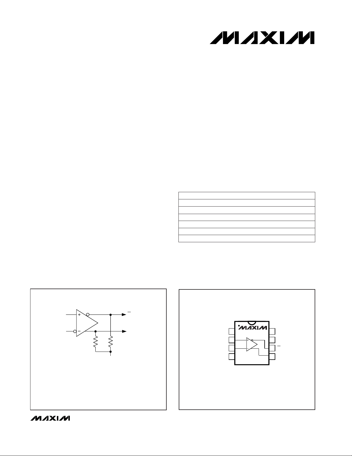
TOP VIEW
MAX9690
DIP/SO
1
2
3
4
8
7
6
5
GND1
GND2
Q OUT
Q OUT
V+
IN+
IN-
V-
__________________Pin Configuration
______________Ordering Information
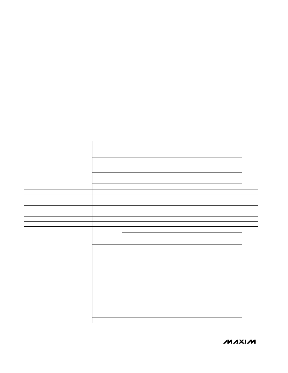
IN+
R
L
R
L
IN-
V
T
Q OUT
Q OUT
THE OUTPUTS ARE OPEN EMITTERS, REQUIRING
EXTERNAL PULL-DOWN RESISTORS. THESE RESISTORS
MAY BE WITHIN 50Ω–200Ω CONNECTED TO -2.0V, OR
240Ω–2kΩ CONNECTED TO -5.2V.
________________Functional Diagram
19-2401; Rev 3; 3/97
PART TEMP. RANGE PIN-PACKAGE
MAX9690CPA-4 0°C to +70°C 8 Plastic DIP
MAX9690CSA 0°C to +70°C 8 SO
MAX9690CJA 0°C to +70°C 8 CERDIP
MAX9690EPA -40°C to +85°C 8 Plastic DIP
MAX9690ESA -40°C to +85°C 8 SO
MAX9690MJA-4 -55°C to +125°C 8 CERDIP
For free samples & the latest literature: http://www.maxim-ic.com, or phone 1-800-998-8800.
For small orders, phone 408-737-7600 ext. 3468.
Page 2
MAX9690
Ultra-Fast ECL-Output Comparator
2 _______________________________________________________________________________________
ABSOLUTE MAXIMUM RATINGS
ELECTRICAL CHARACTERISTICS
(V+ = +5V, V- = -5.2V, RL= 50Ω, VT= -2V, TA= +25°C, unless otherwise noted.)
Stresses beyond those listed under “Absolute Maximum Ratings” may cause permanent damage to the device. These are stress ratings only, and functional
operation of the device at these or any other conditions beyond those indicated in the operational sections of the specifications is not implied. Exposure to
absolute maximum rating conditions for extended periods may affect device reliability.
Common-Mode
Rejection Ratio
CMRR dB
Input Voltage Range V
CM
V
Input Bias Current I
B
µA
Input Offset Current I
OS
µA
Power-Supply
Rejection Ratio
PSRR dB
Input Resistance R
IN
kΩ
Input Capacitance C
IN
pF
V
OH
V
Input Offset Voltage V
OS
mV
Temperature Coefficient ∆VOS/∆T µV/°C
(Note 1)
(Note 1)
TA= +25°C
TA= +25°C
(Note 1)
TA= +25°C
TA= T
MIN
to T
MAX
(Note 1)
80
-2.5 +2.5
10 20
5
60
60
3
-1.05 -0.87
-5 5
-7 7
10
PARAMETER SYMBOL UNITS
MAX9690C/E
MIN TYP MAX
CONDITIONS
80
-2.5 +2.5
10 20
5
60
60
3
-1.16 -0.89
-5 5
-8 8
15
MAX9690M
MIN TYP MAX
-0.88 -0.69-0.89 -0.70
-0.96 -0.81-0.96 -0.81
MAX9690C,
MAX9690M
Positive Supply
Current
16 22
mA
16 22TA= +25°C
2524TA= T
MIN
to T
MAX
Logic Output
High Voltage
-0.88 -0.70
-0.96 -0.81
MAX9690E
-1.14 -0.88
Negative Supply
Current
20 32
mA
20 32TA= +25°C
3736TA= T
MIN
to T
MAX
Logic Output
Low Voltage
-1.83 -1.57
-1.85 -1.65
MAX9690E
-1.90 -1.65
V
OL
-1.82 -1.55
V
-1.90 -1.65-1.89 -1.65
-1.85 -1.65-1.85 -1.65
MAX9690C,
MAX9690M
-1.83 -1.57
Supply Voltages.....................................................................±6V
Input Voltages........................................................................±5V
Differential Input Voltages...................................................±3.5V
Output Current....................................................................30mA
Continuous Power Dissipation (T
A
= +70°C)
Plastic DIP (derate 9.09mW/°C above +70°C)...........727mW
SO (derate 5.88mW/°C above +70°C).......................471mW
CERDIP (derate 8.00mW/°C above +70°C)...............640mW
Operating Temperature Ranges
MAX9690C_ A...................................................0°C to +70°C
MAX9690E_ A................................................-40°C to +85°C
MAX9690MJA ..............................................-55°C to +125°C
Storage Temperature Range.............................-55°C to +150°C
Lead Temperature (soldering, 10sec).............................+300°C
TA= T
MIN
to T
MAX
TA= T
MIN
to T
MAX
8
30
12
40
TA= T
MIN
TA= T
MAX
TA= +25°C
TA= T
MIN
TA= T
MAX
TA= +25°C
TA= T
MIN
TA= T
MAX
TA= T
MIN
TA= T
MAX
TA= +25°C
TA= +25°C
Page 3

MAX9690
Ultra-Fast ECL-Output Comparator
_______________________________________________________________________________________ 3
__________Applications Information
Layout
Because of the MAX9690’s large gain-bandwidth characteristic, special precautions need to be taken if its highspeed capabilities are to be used. A PC board with a
ground plane is mandatory. Mount all decoupling capacitors as close to the power-supply pins as possible, and
process the ECL outputs in microstrip fashion, consistent
with the load termination of 50Ω to 120Ω. For low-impedance applications, microstrip layout at the input may also
be helpful. Pay close attention to the bandwidth of the
decoupling and terminating components. Chip components can be used to minimize lead inductance.
Input Slew-Rate Requirements
As with all high-speed comparators, the high gain-bandwidth product of these devices creates oscillation problems when the input traverses through the linear region.
For clean switching without oscillation or steps in the output waveform, the input must meet certain minimum slewrate requirements. The tendency of the part to oscillate is
a function of the layout and source impedance of the circuit employed. Both poor layout and larger source impedance increase the minimum slew-rate requirement.
____________________Timing Diagram
The timing diagram illustrates the series of events that
completes the compare function, under worst-case
conditions. The leading edge of the input signal (illustrated as a large-amplitude, small-overdrive pulse)
switches the comparator. Outputs –Q–and Q are similar
in timing.
Definition of Terms
V
OS
Input Offset Voltage—The voltage required
between the input terminals to obtain 0V differential at the output.
V
IN
Input Voltage Pulse Amplitude
V
OD
Input Voltage Overdrive
t
pd+
Input to Output High Delay—The propagation
delay measured from the time the input signal
crosses the input offset voltage to the 50% point
of an output low-to-high transition.
t
pd-
Input to Output Low Delay—The propagation
delay measured from the time the input signal
crosses the input offset voltage to the 50% point
of an output high-to-low transition.
SWITCHING CHARACTERISTICS
(V+ = +5V, V- = -5.2V, RL= 50Ω, VT= -2V, TA= +25°C, unless otherwise noted.)
Note 1: Not tested, guaranteed by design.
Note 2: V
IN
= 100mV, VOD= 10mV.
PARAMETER
SYMBOL
MAX9690C/E
MIN TYP MAX
MAX9690M
MIN TYP MAX
UNITS
1.3 1.8 1.3 1.8
1.5 2.0
Input to Output High
(Notes 1, 2)
t
pd+
1.7 2.4
ns
1.3 1.8 1.3 1.8
1.5 2.0
CONDITIONS
TA= +25°C
TA= 0°C to +70°C
TA= -55°C to +125°C
TA= +25°C
TA= 0°C to +70°C
Input to Output Low
(Notes 1, 2)
t
pd-
1.7 2.4
ns
TA= -55°C to +125°C
Page 4

MAX9690
Ultra-Fast ECL-Output Comparator
DIFFERENTIAL
INPUT
VOLTAGE
Q
Q
V
OD
V
IN
V
OS
50%
50%
t
pd
Figure 1. Timing Diagram
Maxim cannot assume responsibility for use of any circuitry other than circuitry entirely embodied in a Maxim product. No circuit patent licenses are
implied. Maxim reserves the right to change the circuitry and specifications without notice at any time.
4
_____________________Maxim Integrated Products, 120 San Gabriel Drive, Sunnyvale, CA 94086 408-737-7600
© 1997 Maxim Integrated Products Printed USA is a registered trademark of Maxim Integrated Products.
 Loading...