

Page 1
For free samples & the latest literature: http://www.maxim-ic.com, or phone 1-800-998-8800.
For small orders, phone 408-737-7600 ext. 3468.
__________________General Description
The MAX8877/MAX8878 low-noise, low-dropout linear
regulators operate from a 2.5V to 6.5V input and deliver
up to 150mA. These devices are pin-compatible with
the industry-standard ‘2982 and offer an improved
dropout voltage. Typical output noise is 30µV
RMS
, and
typical dropout is only 165mV at 150mA. The output
voltage is preset to voltages in the range of 2.5V to
5.0V, in 100mV increments.
Designed with an internal P-channel MOSFET pass
transistor, the MAX8877/MAX8878 maintain a low
100µA supply current, independent of the load current
and dropout voltage. Other features include a 10nA
logic-controlled shutdown mode, short-circuit and thermal-shutdown protection, and reverse battery protection. The MAX8878 also includes an auto-discharge
function, which actively discharges the output voltage
to ground when the device is placed in shutdown. Both
devices come in a miniature 5-pin SOT23 package.
________________________Applications
Cellular Telephones
Cordless Telephones
PCS Telephones
PCMCIA Cards
Modems
Hand-Held Instruments
Palmtop Computers
Electronic Planners
____________________________Features
♦ Pin-Compatible with the Industry-Standard ‘2982
♦ Low Output Noise: 30µV
RMS
♦ Low 55mV Dropout at 50mA Output
(165mV at 150mA output)
♦ Low 85µA No-Load Supply Current
♦ Low 100µA Operating Supply Current
(even in dropout)
♦ Thermal-Overload and Short-Circuit Protection
♦ Reverse Battery Protection
♦ Output Current Limit
♦ Preset Output Voltages (±1.4% Accuracy)
♦ 10nA Logic-Controlled Shutdown
MAX8877/MAX8878
Low-Noise, Low-Dropout, 150mA Linear
Regulators with ‘2982 Pinout
________________________________________________________________
Maxim Integrated Products
1
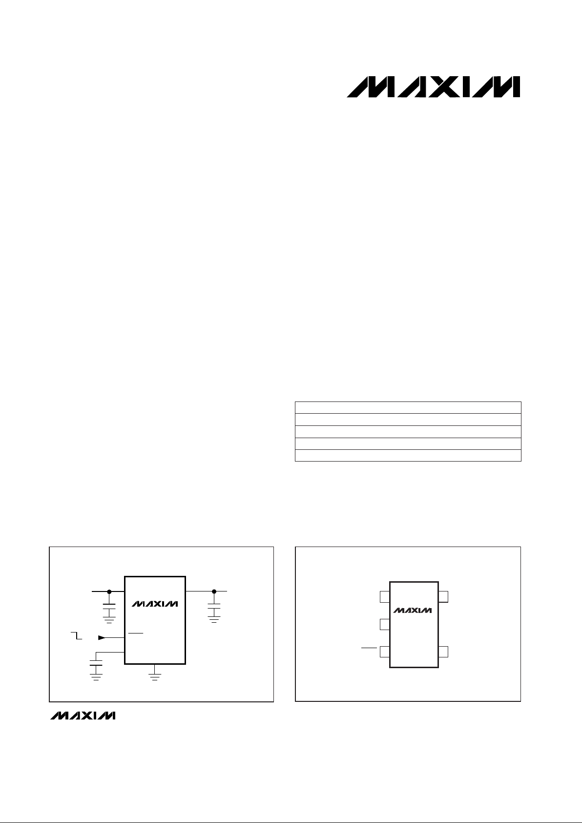
GND
BP
SHDN
1
5
OUT
IN
MAX8877
MAX8878
SOT23-5
TOP VIEW
2
3
4
_____________________Pin Configuration
MAX8877
MAX8878
INPUT
2.5V TO 6.5V
IN OUT
SHDN
BP
GND
OUTPUT
PRESET
2.5V TO 5.0V
150mA
C
BP
0.01µF
C
OUT
1µF
C
IN
1µF
OFF
ON
____________Typical Operating Circuit
19-1301; Rev 1; 3/98
PART**
MAX8877C/Dxy
MAX8877EUKxy-T
MAX8878C/Dxy
0°C to +70°C
-40°C to +85°C
0°C to +70°C
TEMP. RANGE PIN-PACKAGE
Dice*
5 SOT23-5
Dice*
_________________Ordering Information
*
Dice are tested at TA= +25°C only.
**
xy is the output voltage code (see Expanded Ordering
Information table at end of data sheet).
MAX8878EUKxy-T -40°C to +85°C 5 SOT23-5
Page 2
MAX8877/MAX8878
Low-Noise, Low-Dropout, 150mA Linear
Regulators with ‘2982 Pinout
2 _______________________________________________________________________________________
ABSOLUTE MAXIMUM RATINGS
ELECTRICAL CHARACTERISTICS
(VIN= V
OUT(NOMINAL)
+ 0.5V, TA= -40°C to +85°C, unless otherwise noted. Typical values are at TA= +25°C.) (Note 1)
Stresses beyond those listed under “Absolute Maximum Ratings” may cause permanent damage to the device. These are stress ratings only, and functional
operation of the device at these or any other conditions beyond those indicated in the operational sections of the specifications is not implied. Exposure to
absolute maximum rating conditions for extended periods may affect device reliability.
Note 1: Limits are 100% production tested at TA= +25°C. Limits over the operating temperature range are guaranteed through
correlation using Statistical Quality Control (SQC) Methods.
Note 2: The dropout voltage is defined as V
IN
- V
OUT
, when V
OUT
is 100mV below the value of V
OUT
for VIN= V
OUT
+ 0.5V.
Note 3: Time needed for V
OUT
to reach 95% of final value.
IN to GND....................................................................-7V to +7V
Output Short-Circuit Duration ............................................Infinite
SHDN to GND..............................................................-7V to +7V
SHDN to IN...............................................................-7V to +0.3V
OUT, BP to GND..........................................-0.3V to (V
IN
+ 0.3V)
Continuous Power Dissipation (TA= +70°C)
SOT23-5 (derate 7.1mW/°C above +70°C)..................571mW
Operating Temperature Range ...........................-40°C to +85°C
Junction Temperature......................................................+150°C
θ
JB
..................................................................................140°C/W
Storage Temperature.........................................-65°C to +160°C
Lead Temperature (soldering, 10sec).............................+300°C
MAX8878 only
CBP= 0.1µF
C
OUT
= 1µF, no load
I
OUT
= 0mA, TA= +25°C
V
OUT
= 0V
V
SHDN
= V
IN
VIN= 2.5V to 5.5V
I
OUT
= 0mA to 120mA, C
OUT
= 1µF
VIN= 2.5V to 5.5V
I
OUT
= 150mA
I
OUT
= 50mA
No load
I
OUT
= 150mA
I
OUT
= 1mA
f = 10Hz to 100kHz,
CBP= 0.01µF
CONDITIONS
Ω300Resistance Shutdown Discharge
300
µs
30 150
Shutdown Exit Delay
(Note 3)
0.2
µA
0.01 1
I
Q(SHDN)
Shutdown Supply Current
0.5
nA
0.01 100
I
SHDN
SHDN Input Bias Current
0.4V
IL
V
2.0V
IH
SHDN Input Threshold
20
µV
RMS
30
e
n
Output Voltage Noise
mA150Maximum Output Current
-1.4 1.4
V2.5 6.5V
IN
Input Voltage
%/mA0.01 0.04∆V
LDR
Load Regulation
165
55 120
mA160 390I
LIM
Current Limit
µA
85 180
I
Q
Ground Pin Current
100
mV
1.1
Dropout Voltage (Note 2)
UNITSMIN TYP MAXSYMBOLPARAMETER
TA= -40°C to +85°C
TA= +25°C
TA= +85°C
TA= +25°C
TA= +85°C
TA= +25°C
C
OUT
= 100µF
C
OUT
= 10µF
°C155T
SHDN
Thermal Shutdown Temperature
°C15∆T
SHDN
Thermal Shutdown Hysteresis
I
OUT
= 0mA to 120mA, TA= -40°C to +85°C
%
-3 2
Output Voltage Accuracy
VIN= (V
OUT
+ 0.1V) to 6.5V, I
OUT
= 1mA %/V-0.15 0 0.15∆V
LNR
Line Regulation
SHUTDOWN
THERMAL PROTECTION
Page 3
MAX8877/MAX8878
Low-Noise, Low-Dropout, 150mA Linear
Regulators with ‘2982 Pinout
_______________________________________________________________________________________
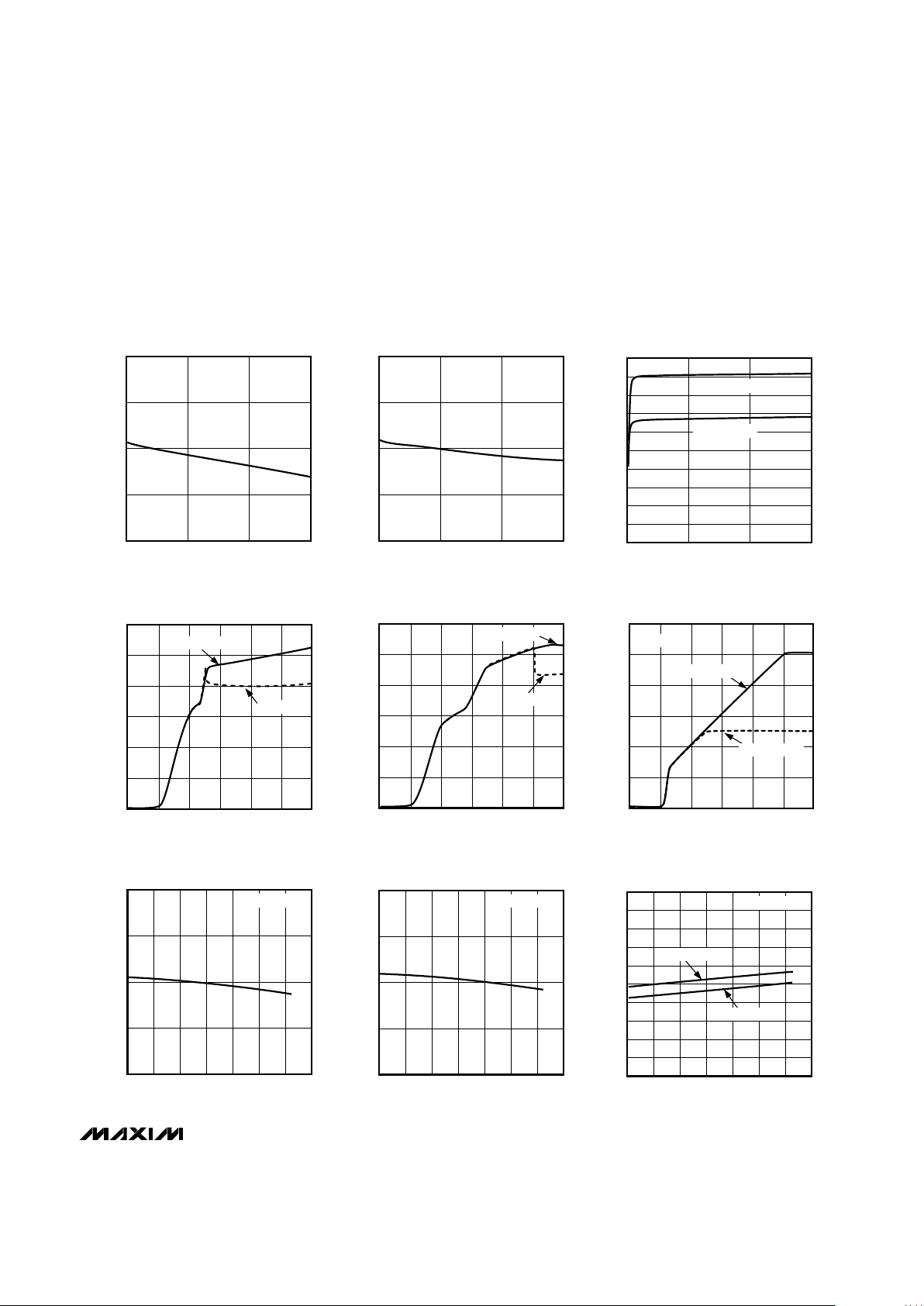
3
2.40
2.45
2.50
2.55
2.60
0 50 100 150
OUTPUT VOLTAGE vs. LOAD CURRENT
(MAX887_EUK25)
MAX8877-01
LOAD CURRENT (mA)
OUTPUT VOLTAGE (V)
4.8
4.9
5.0
5.1
5.2
0 50 100 150
OUTPUT VOLTAGE vs. LOAD CURRENT
(MAX887_EUK50)
MAX8877-02
LOAD CURRENT (mA)
OUTPUT VOLTAGE (V)
60
65
70
75
80
85
90
95
100
105
110
0 50 100 150
GROUND PIN CURRENT
vs. LOAD CURRENT
MAX8877-03
LOAD CURRENT (mA)
GROUND PIN CURRENT (µA)
MAX887_EUK50
MAX887_EUK25
0
40
20
80
60
100
120
0 2 31 4 5 6
GROUND PIN CURRENT vs. INPUT VOLTAGE
(MAX887_EUK25)
MAX8877-04
INPUT VOLTAGE (V)
GROUND PIN CURRENT (µA)
NO LOAD
I
LOAD
= 50mA
2.40
2.45
2.50
2.55
2.60
-40 40200-20 60 80 100
OUTPUT VOLTAGE vs. TEMPERATURE
(MAX887_EUK25)
MAX8877-07
TEMPERATURE (°C)
OUTPUT VOLTAGE (V)
I
LOAD
= 50mA
0
40
20
80
60
100
120
0 2 31 4 5 6
GROUND PIN CURRENT vs. INPUT VOLTAGE
(MAX887_EUK50)
MAX8877-05
INPUT VOLTAGE (V)
GROUND PIN CURRENT (µA)
NO LOAD
I
LOAD
= 50mA
0
2
1
4
3
5
6
0 2 31 4 5 6
OUTPUT VOLTAGE vs. INPUT VOLTAGE
MAX8877-06
INPUT VOLTAGE (V)
OUTPUT VOLTAGE (V)
MAX887_EUK25
NO LOAD
MAX887_EUK50
4.8
4.9
5.0
5.1
5.2
-40 40200-20 60 80 100
OUTPUT VOLTAGE vs. TEMPERATURE
(MAX887_EUK50)
MAX8877-08
TEMPERATURE (°C)
OUTPUT VOLTAGE (V)
I
LOAD
= 50mA
0
60
40
20
100
80
180
160
140
120
200
-40 -20 0 20 40 60 80 100
GROUND PIN CURRENT
vs. TEMPERATURE
MAX8877-09
TEMPERATURE (°C)
GROUND PIN CURRENT (µA)
MAX887_EUK50
MAX887_EUK25
I
LOAD
= 50mA
__________________________________________Typical Operating Characteristics
(VIN= V
OUT(NOMINAL)
+ 0.5V, CIN= 1µF, C
OUT
= 1µF, CBP= 0.01µF, TA= +25°C, unless otherwise noted.)
Page 4

MAX8877/MAX8878
Low-Noise, Low-Dropout, 150mA Linear
Regulators with ‘2982 Pinout
4 _______________________________________________________________________________________
____________________________Typical Operating Characteristics (continued)
(VIN= V
OUT(NOMINAL)
+ 0.5V, CIN= 1µF, C
OUT
= 1µF, CBP= 0.01µF, TA= +25°C, unless otherwise noted.)
0
50
150
100
200
250
0 40 6020 80 100 120 140 160
DROPOUT VOLTAGE vs. LOAD CURRENT
(MAX887_EUK25)
MAX8877-10
LOAD CURRENT (mA)
DROPOUT VOLTAGE (mV)
TA = +85°C
TA = +25°C
TA = -40°C
0
50
100
150
200
0 40 6020 80 100 120 140 160
DROPOUT VOLTAGE vs. LOAD CURRENT
(MAX887_EUK50)
MAX8877-11
LOAD CURRENT (mA)
DROPOUT VOLTAGE (mV)
TA = +85°C
TA = +25°C
TA = -40°C
70
0
10
20
30
40
50
60
0.01 0.1 1 10 100 1000
POWER-SUPPLY REJECTION RATIO
vs. FREQUENCY
MAX8877-12
FREQUENCY (kHz)
PSRR (dB)
I
LOAD
= 50mA
C
BP
= 0.1µF
C
OUT
= 10µF
C
OUT
= 1µF
10
0.01
0 101 1000
OUTPUT NOISE SPECTRAL DENSITY
vs. FREQUENCY
0.1
1
MAX8877-13
FREQUENCY (kHz)
OUTPUT NOISE SPECTRAL DENSITY (µV/√Hz)
100
CBP = 0.01µF
I
LOAD
= 10mA
C
OUT
= 10µF
C
OUT
= 1µF
1ms/div
MAX887_EUK25, C
OUT
= 10µF, I
LOAD
= 10mA, CBP = 0.1µF
OUTPUT NOISE 10Hz TO 100kHz
V
OUT
50µV/div
MAX8877-16
80
0
10
20
30
40
50
60
70
0.001 0.01 0.1
OUTPUT NOISE vs. BP CAPACITANCE
MAX8877-14
BP CAPACITANCE (µF)
OUTPUT NOISE (µV
RMS
)
MAX887_EUK50
C
OUT
= 10µF
I
LOAD
= 10mA
f = 10Hz to 100kHz
MAX887_EUK30
MAX887_EUK25
0
20
10
40
30
50
60
1 10 100 1000
OUTPUT NOISE vs. LOAD CURRENT
MAX8877-15
LOAD CURRENT (mA)
OUTPUT NOISE (µV
RMS
)
MAX887_EUK50
C
OUT
= 10µF
C
BP
= 0.01µF
f = 10Hz to 100kHz
MAX887_EUK30
MAX887_EUK25
100
0.01
0 100 150
REGION OF STABLE C
OUT
ESR
vs. LOAD CURRENT
0.1
MAX8877-17
LOAD CURRENT (mA)
C
OUT
ESR (Ω)
1
10
C
OUT
= 10µF
C
OUT
= 1µF
STABLE REGION
Page 5

MAX8877/MAX8878
Low-Noise, Low-Dropout, 150mA Linear
Regulators with ‘2982 Pinout
_______________________________________________________________________________________
5
3.00V
2.99V
3.01V
V
OUT
I
LOAD
50mA
10µs/div
LOAD-TRANSIENT RESPONSE
MAX8877-19
MAX887_EUK30, VIN = V
OUT
+ 0.5V,
C
IN
= 10µF, I
LOAD
= 0mA TO 50mA
3.00V
2.99V
3.01V
V
OUT
I
LOAD
50mA
10µs/div
LOAD-TRANSIENT RESPONSE
NEAR DROPOUT
MAX8877-20
MAX887_EUK30, VIN = V
OUT
+ 0.1V,
C
IN
= 10µF, I
LOAD
= 0mA TO 50mA
1V
0V
0V
2V
2V
5µs/div
MAX887_EUK25
SHUTDOWN EXIT DELAY
MAX8877-21
MAX887_EUK25, I
LOAD
= 50mA
V
SHDN
V
OUT
CBP = 0.01µF
CBP = 0.1µF
0V
0V
4V
2V
2V
5µs/div
MAX887_EUK50
SHUTDOWN EXIT DELAY
MAX8877-22
MAX887_EUK50, I
LOAD
= 50mA
V
SHDN
V
OUT
CBP = 0.01µF
CBP = 0.1µF
0V
0V
5V
2V
V
SHDN
V
OUT
500µs/div
ENTERING SHUTDOWN
MAX8877-23
MAX8878, NO LOAD
____________________________Typical Operating Characteristics (continued)
(VIN= V
OUT(NOMINAL)
+ 0.5V, CIN= 1µF, C
OUT
= 1µF, CBP= 0.01µF, TA= +25°C, unless otherwise noted.)
3.000V
2.999V
3.001V
3V
4V
V
IN
V
OUT
100µs/div
LINE-TRANSIENT RESPONSE
MAX8877-18
MAX887_EUK30, I
LOAD
= 50mA
______________________________________________________________Pin Description
NAME FUNCTION
1 IN
Regulator Input. Supply voltage can range from 2.5V to 6.5V. Bypass with a 1µF capacitor to GND (see
Capacitor Selection and Regulator Stability
section).
2 GND
Ground. This pin also functions as a heatsink. Solder to a large pad or the circuit-board ground plane to
maximize power dissipation.
PIN
3
SHDN
Active-Low Shutdown Input. A logic low reduces the supply current to 10nA. On the MAX8878, a logic low
also causes the output voltage to discharge to GND. Connect to IN for normal operation.
4 BP
Reference-Noise Bypass. Bypass with a low-leakage, 0.01µF ceramic capacitor for reduced noise at the
output.
5 OUT Regulator Output. Sources up to 150mA. Bypass with a 1µF (<0.2Ω typical ESR) capacitor to GND.
Page 6

MAX8877/MAX8878
_______________Detailed Description
The MAX8877/MAX8878 are low-noise, low-dropout,
low-quiescent-current linear regulators designed primarily for battery-powered applications. The parts are
available with preset output voltages ranging from 2.5V
to 5V, in 100mV increments. These devices can supply
loads up to 150mA. As illustrated in Figure 1, the
MAX8877/MAX8878 consist of a 1.25V reference, error
amplifier, P-channel pass transistor, and internal feedback voltage divider.
The 1.25V bandgap reference is connected to the error
amplifier’s inverting input. The error amplifier compares
this reference with the feedback voltage and amplifies
the difference. If the feedback voltage is lower than the
reference voltage, the pass-transistor gate is pulled
lower, which allows more current to pass to the output
and increases the output voltage. If the feedback voltage is too high, the pass-transistor gate is pulled up,
allowing less current to pass to the output. The output
voltage is fed back through an internal resistor voltage
divider connected to the OUT pin.
An external bypass capacitor connected to the BP pin
reduces noise at the output. Additional blocks include a
current limiter, reverse battery protection, thermal sensor, and shutdown logic. The MAX8878 also includes
an auto-discharge function, which actively discharges
the output voltage to ground when the device is placed
in shutdown mode.
Output Voltage
The MAX8877/MAX8878 are supplied with factory-set
output voltages from 2.5V to 5.0V, in 100mV increments.
Except for the MAX887_EUK29 and the MAX887_EUK32
(which have an output voltage preset at 2.84V and
3.15V, respectively), the two-digit suffix allows the customer to choose the output voltage in 100mV increments.
For example, the MAX8877EUK33 has a preset output
voltage of 3.3V (see
Expanded Ordering Information
).
Internal P-Channel Pass Transistor
The MAX8877/MAX8878 feature a 1.1Ω typical
P-channel MOSFET pass transistor. This provides several advantages over similar designs using PNP pass transistors, including longer battery life. The P-channel
MOSFET requires no base drive, which reduces quiescent current considerably. PNP-based regulators waste
considerable current in dropout when the pass transistor
saturates. They also use high base-drive currents under
large loads. The MAX8877/MAX8878 do not suffer from
these problems and consume only 100µA of quiescent
current whether in dropout, light-load, or heavy-load
applications (see the
Typical Operating Characteristics
).
Current Limit
The MAX8877/MAX8878 include a current limiter, which
monitors and controls the pass transistor’s gate voltage,
limiting the output current to 390mA. For design purposes,
consider the current limit to be 160mA minimum to 500mA
maximum. The output can be shorted to ground for an
indefinite amount of time without damaging the part.
Low-Noise, Low-Dropout, 150mA Linear
Regulators with ‘2982 Pinout
6 _______________________________________________________________________________________
SHUTDOWN
AND
POWER-ON
CONTROL
ERROR
AMP
1.25V
REF
P
N
*
OUT
BP
* AUTO-DISCHARGE, MAX8878 ONLY
GND
IN
SHDN
MAX8877
MAX8878
MOS DRIVER
WITH I
LIMIT
THERMAL
SENSOR
REVERSE
BATTERY
PROTECTION
Figure 1. Functional Diagram
Page 7

Thermal-Overload Protection
Thermal-overload protection limits total power dissipation in the MAX8877/MAX8878. When the junction temperature exceeds TJ= +155°C, the thermal sensor
signals the shutdown logic, turning off the pass transistor and allowing the IC to cool. The thermal sensor will
turn the pass transistor on again after the IC’s junction
temperature cools by 15°C, resulting in a pulsed output
during continuous thermal-overload conditions.
Thermal-overload protection is designed to protect the
MAX8877/MAX8878 in the event of fault conditions. For
continual operation, do not exceed the absolute maximum junction-temperature rating of TJ= +150°C.
Operating Region and Power Dissipation
The MAX8877/MAX8878’s maximum power dissipation
depends on the thermal resistance of the case and circuit
board, the temperature difference between the die junction and ambient air, and the rate of air flow. The power
dissipation across the device is P = I
OUT(VIN
- V
OUT
).
The maximum power dissipation is:
P
MAX
= (TJ- TA) / (θJB+ θBA)
where TJ- TAis the temperature difference between
the MAX8877/MAX8878 die junction and the surrounding air, θJB(or θJC) is the thermal resistance of the
package, and θBAis the thermal resistance through the
printed circuit board, copper traces, and other materials to the surrounding air.
The GND pin of the MAX8877/MAX8878 performs the
dual function of providing an electrical connection to
ground and channeling heat away. Connect the GND
pin to ground using a large pad or ground plane.
Reverse Battery Protection
The MAX8877/MAX8878 have a unique protection
scheme that limits the reverse supply current to 1mA
when either VINor V
SHDN
falls below ground. Their circuitry monitors the polarity of these two pins and disconnects the internal circuitry and parasitic diodes when the
battery is reversed. This feature prevents device damage.
Noise Reduction
An external 0.01µF bypass capacitor at BP, in conjunction with an internal 200kΩ resistor, creates a 80Hz lowpass filter for noise reduction. The MAX8877/MAX8878
exhibit 30µV
RMS
of output voltage noise with CBP=
0.01µF and C
OUT
= 10µF. This is negligible in most
applications. Start-up time is minimized by a power-on
circuit that pre-charges the bypass capacitor. The
Typical Operating Characteristics
section shows
graphs of Noise vs. BP Capacitance, Noise vs. Load
Current, and Output Noise Spectral Density.
____________Applications Information
Capacitor Selection and
Regulator Stability
Normally, use a 1µF capacitor on the MAX8877/
MAX8878’s input and a 1µF to 10µF capacitor on the output. Larger input capacitor values and lower ESRs provide better supply-noise rejection and line-transient
response. Reduce noise and improve load-transient
response, stability, and power-supply rejection by using
large output capacitors. For stable operation over the full
temperature range and with load currents up to 150mA, a
minimum of 1µF is recommended.
Note that some ceramic dielectrics exhibit large capacitance and ESR variation with temperature. With
dielectrics such as Z5U and Y5V, it may be necessary to
use 2.2µF or more to ensure stability at temperatures
below -10°C. With X7R or X5R dielectrics, 1µF should be
sufficient at all operating temperatures. Also, for high-ESR
tantalum capacitors, 2.2µF or more may be needed to
maintain ESR in the stable region. A graph of the Region
of Stable C
OUT
ESR vs. Load Current is shown in the
Typical Operating Characteristics
.
Use a 0.01µF bypass capacitor at BP for low output voltage noise. Increasing the capacitance will slightly
decrease the output noise, but increase the start-up time.
Values above 0.1µF provide no performance advantage
and are not recommended (see Shutdown Exit Delay
graphs in the
Typical Operating Characteristics
).
PSRR and Operation from
Sources Other than Batteries
The MAX8877/MAX8878 are designed to deliver low
dropout voltages and low quiescent currents in batterypowered systems. Power-supply rejection is 63dB at
low frequencies and rolls off above 10kHz. See the
Power-Supply Rejection Ratio Frequency graph in the
Typical Operating Characteristics
.
When operating from sources other than batteries,
improved supply-noise rejection and transient response
can be achieved by increasing the values of the input
and output bypass capacitors, and through passive filtering techniques. The
Typical Operating Charac-
teristics
show the MAX8877/MAX8878’s line- and load-
transient responses.
Load-Transient Considerations
The MAX8877/MAX8878 load-transient response
graphs (see
Typical Operating Characteristics
) show
two components of the output response: a DC shift
from the output impedance due to the load current
change, and the transient response. Typical transient
MAX8877/MAX8878
Low-Noise, Low-Dropout, 150mA Linear
Regulators with ‘2982 Pinout
_______________________________________________________________________________________ 7
Page 8

MAX8877/MAX8878
Low-Noise, Low-Dropout, 150mA Linear
Regulators with ‘2982 Pinout
Maxim cannot assume responsibility for use of any circuitry other than circuitry entirely embodied in a Maxim product. No circuit patent licenses are
implied. Maxim reserves the right to change the circuitry and specifications without notice at any time.
8
_____________________Maxim Integrated Products, 120 San Gabriel Drive, Sunnyvale, CA 94086 408-737-7600
© 1998 Maxim Integrated Products Printed USA is a registered trademark of Maxim Integrated Products.
for a step change in the load current from 0mA to 50mA
is 12mV. Increasing the output capacitor’s value and
decreasing the ESR attenuates the overshoot.
Input-Output (Dropout) Voltage
A regulator’s minimum input-output voltage differential
(or dropout voltage) determines the lowest usable sup-
ply voltage. In battery-powered systems, this will determine the useful end-of-life battery voltage. Because the
MAX8877/MAX8878 use a P-channel MOSFET pass
transistor, their dropout voltage is a function of drain-tosource on-resistance (R
DS(ON)
) multiplied by the load
current (see
Typical Operating Characteristics
).
____________________________________________Expanded Ordering Information
___________________Chip Information
OUTPUT VOLTAGE (xy)
CODE
PRESET OUTPUT
VOLTAGE (V)
SOT TOP MARK
MAX8877 MAX8878
MAX887_EUK25-T 2.50 ACBM ACBT
MAX887_EUK28-T 2.80 ACBN ACBU
MAX887_EUK29-T 2.84 ACBO ACBV
MAX887_EUK30-T 3.00 ACBP ACBW
MAX887_EUK32-T 3.15 ACBQ ACBX
MAX887_EUK33-T 3.30 ACBR ACBY
MAX887_EUK50-T 5.00 ACBS ACBZ
Other xy*** x.y0 — —
***
Other xy between 2.5V and 5.0V are available in 100mV increments. Contact factory for other versions. Minimum order quantity is 25,000 units.
________________________________________________________Package Information
SOT5L.EPS
MAX887_EUK36-T 3.60 ACDB ACDC
TRANSISTOR COUNT: 247
SUBSTRATE CONNECTED TO GND
 Loading...