

Datasheet MAX8875EUK25-T, MAX8875EUK27-T, MAX8875EUK30-T, MAX8875EUK50-T, MAX8875EUK33-T Datasheet (Maxim)
Page 1
For free samples & the latest literature: http://www.maxim-ic.com, or phone 1-800-998-8800.
For small orders, phone 1-800-835-8769.
General Description
The MAX8875 low-dropout linear regulator operates from
a +2.5V to +6.5V input range and delivers up to 150mA.
A P-channel MOSFET pass transistor allows its 85µA supply current to remain independent of the load, making this
device ideal for battery-operated portable equipment
such as PCS phones, cellular phones, cordless phones,
and modems.
The MAX8875 features a power-OK output that indicates
when the output is out of regulation. The device is available in several preset output voltage versions: 5.0V, 3.3V,
3.0V, 2.7V, or 2.5V. Other features include 1µA (max) shutdown current, short-circuit protection, thermal shutdown
protection, and reverse-battery protection. The device
comes in a miniature 5-pin SOT23 package.
The MAX8875 is optimized for use with a 1µF ceramic output capacitor. For a pin-compatible, functionally equivalent
device for use with a higher ESR output capacitor, see the
MAX8885 data sheet.
Applications
PCS Telephones Hand-Held Instruments
Cellular Telephones Palmtop Computers
Cordless Telephones Electronic Planners
PCMCIA Cards Modems
Features
♦ Power-OK Output
♦ Small Output Capacitor (1µF ceramic)
♦ Preset Output Voltages (±1% accuracy)
♦ Guaranteed 150mA Output Current
♦ 85µA No-Load Supply Current
♦ Low 110mV Dropout at 100mA Load (165mV at
150mA load)
♦ Thermal-Overload and Short-Circuit Protection
♦ Reverse-Battery Protection
♦ 60dB PSRR at 100Hz
♦ 1µA max Shutdown Current
MAX8875
150mA, Low-Dropout Linear Regulator
with Power-OK Output
________________________________________________________________ Maxim Integrated Products 1
Typical Operating Circuit
19-1556; Rev 0; 10/99
PART
MAX8875EUK25-T
MAX8875EUK27-T
MAX8875EUK30-T -40°C to +85°C
-40°C to +85°C
-40°C to +85°C
TEMP. RANGE PIN-PACKAGE
5 SOT23-5
5 SOT23-5
5 SOT23-5
Note: See Output Voltage Selector Guide for more information.
Note: Other output voltages between 2.5V and 5.0V are avail-
able in 100mV increments—contact the factory for information.
Minimum order quantity is 25,000 units.
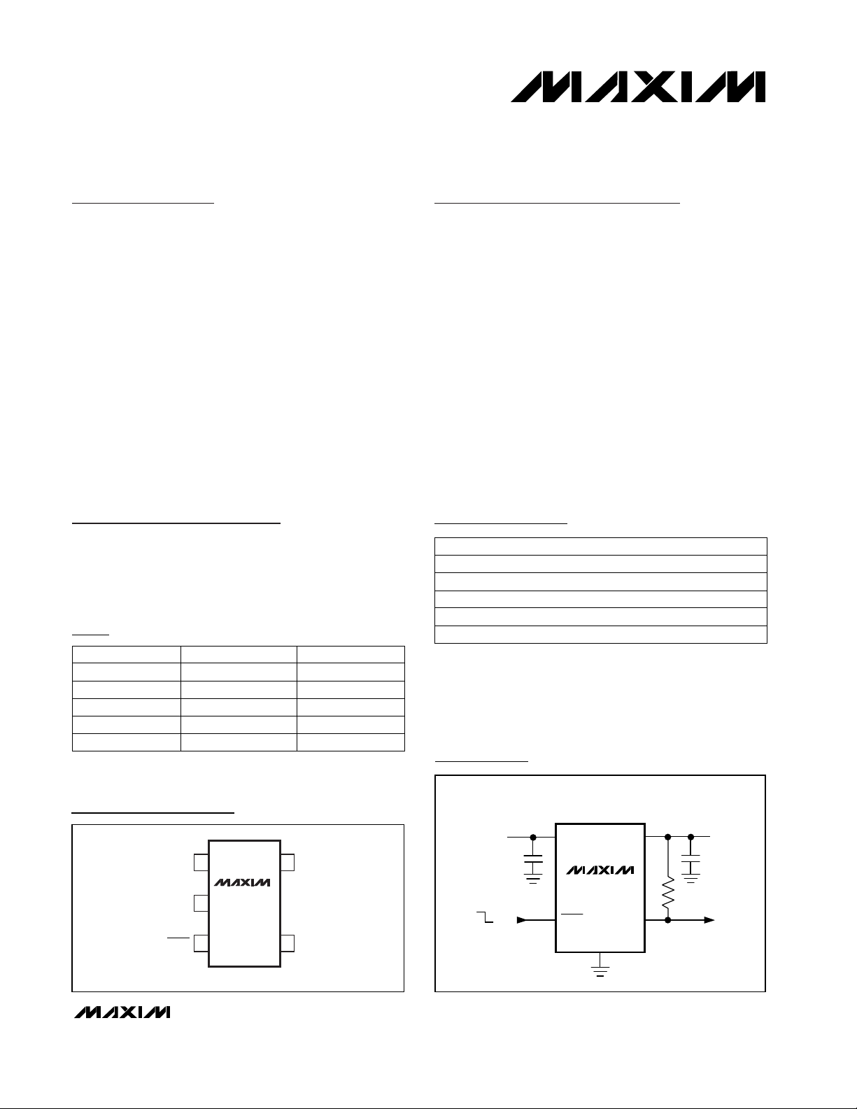
Pin Configuration
Ordering Information
Output Voltage Selector Guide
MAX8875EUK33-T
MAX8875EUK50-T -40°C to +85°C
-40°C to +85°C 5 SOT23-5
5 SOT23-5
MAX8875EUK50
MAX8875EUK33
MAX8875EUK30
MAX8875EUK27
MAX8875EUK25
PART V
OUT
(V)
2.5
2.7
3.0
3.3
5.0 ADLD
ADLC
ADLB
ADLA
ADKZ
TOP MARK
TOP VIEW
1
IN
2
GND
3
SHDN
5
OUT
MAX8875
POK
4
OUTPUT
100k
PRESET
2.5V TO 5.0V
150mA
C
OUT
1µF
TO µC
INPUT
+2.5V TO +6.5V
ON
OFF
C
1µF
IN OUT
IN
MAX8875
SHDN
POK
GND
SOT23-5
Page 2
MAX8875
150mA, Low-Dropout Linear Regulator
with Power-OK Output
2 _______________________________________________________________________________________
ABSOLUTE MAXIMUM RATINGS
ELECTRICAL CHARACTERISTICS
(V
IN
=
V
OUT(NOMINAL)
+ 1V, SHDN = IN, TA= -40°C to +85°C, unless otherwise noted. Typical values are at TA= +25°C.) (Note 1)
Stresses beyond those listed under “Absolute Maximum Ratings” may cause permanent damage to the device. These are stress ratings only, and functional
operation of the device at these or any other conditions beyond those indicated in the operational sections of the specifications is not implied. Exposure to
absolute maximum rating conditions for extended periods may affect device reliability.
IN, SHDN, POK to GND...............................................-7V to +7V
SHDN to IN ...............................................................-7V to +0.3V
OUT to GND ................................................-0.3V to (V
IN
+ 0.3V)
Output Short-Circuit Duration ........................................Indefinite
Continuous Power Dissipation (TA= +70°C)
5-Pin SOT23 (derate 7.1mW/°C above +70°C)..........571mW
Operating Temperature Range ...........................-40°C to +85°C
Junction Temperature......................................................+150°C
θ
JA
...............................................................................+140°C/W
Storage Temperature Range .............................-65°C to +150°C
Lead Temperature (soldering, 10s) .................................+300°C
TA= -40°C to +85°C
-3 2
SHDN Input Threshold
(1 - V
OUT/VOUT(NOMINAL)
100, I
OUT
= 0,
V
OUT
falling
SHDN = IN or GND
TA= +25°C, I
OUT
= 100µA
VIN= 2.5V to 5.5V
TA= +25°C
SHDN = GND
I
OUT
= 150mA
I
OUT
= 100mA
f = 100Hz
C
OUT
= 10µF, f = 10Hz to 100kHz
I
OUT
= 50mA
I
OUT
= 100µA
I
OUT
= 100µA
I
OUT
= 100µA to 120mA, C
OUT
= 1µF
I
OUT
= 150mA
VIN= (V
OUT
+ 0.1V) to 6.5V, I
OUT
= 1mA
CONDITIONS
%
-3 -5 -8
V
POK
Power-OK Voltage Threshold
0.05
nA
0100
I
SHDN
SHDN Input Bias Current
0.4
V
IL
V
2.0
V
IH
0.02
TA= +85°C
µA
0.005 1
I
OFF
Shutdown Supply Current
dB
60
PSRR
Output Voltage AC PowerSupply Rejection Ratio
µV
RMS
170
Output Voltage Noise
%/mA
0.01
∆V
LDR
Load Regulation
%/V
-0.15 0 0.15
∆V
LNR
Line Regulation
-2 2
TA= +25°C
TA= +85°C
%
-1.0 1.0
V
2.5 6.5
V
IN
Input Voltage
Output Voltage Accuracy
165
110 220
mV
50
0.1
V
IN -VOUT
Dropout Voltage (Note 2)
mA
150
I
OUT
Maximum Output Current
mA
160 390
I
LIM
Current Limit
µA
85 180
I
Q
Ground Pin Current
100
UNITSMIN TYP MAXSYMBOLPARAMETER
Hysteresis, I
OUT
= 0
In dropout, V
OUT
falling
1
-5.3
I
OUT
= 100µA to
120mA
I
OUT
= 100µA
SHUTDOWN
POWER-OK OUTPUT
Page 3
MAX8875
150mA, Low-Dropout Linear Regulator
with Power-OK Output
_______________________________________________________________________________________ 3
5
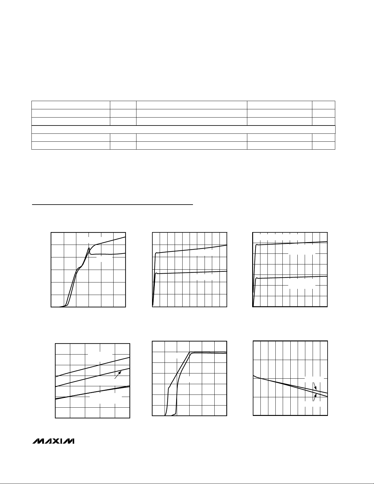
Typical Operating Characteristics
(MAX8875EUK30, VIN= +3.6V, CIN= C
OUT
= 1µF, SHDN = IN, TA= +25°C, unless otherwise noted.)
ELECTRICAL CHARACTERISTICS (continued)
(VIN= V
OUT(NOMINAL)
+ 1V, SHDN = IN, TA= -40°C to +85°C, unless otherwise noted. Typical values are at TA= +25°C.) (Note 1)
Note 1: Limits are 100% production tested at T
A
= +25°C. Limits over the operating temperature range are guaranteed through
correlation using Statistical Quality Control (SQC) methods.
Note 2: Dropout voltage is defined as V
IN
- V
OUT
, when V
OUT
is 100mV below the value of V
OUT
for VIN= V
OUT
+ 0.5V.
POK Output Voltage Low V
OL
0.4
V
Thermal Shutdown Temperature T
SHDN
170
°C
Thermal Shutdown Hysteresis ∆T
SHDN
20
°C
I
SINK
= 1mA
PARAMETER SYMBOL MIN TYP MAX UNITSCONDITIONS
POK Output Leakage Current
1
µA0 ≤ V
POK
≤ 6.5V, V
OUT
in regulation
THERMAL PROTECTION
GROUND PIN CURRENT vs.
INPUT VOLTAGE
120
I
= 150mA
100
80
60
40
GROUND PIN CURRENT (µA)
20
OUT
MAX8875toc01
I
= 0
OUT
GROUND PIN CURRENT vs.
OUTPUT LOAD
115
110
105
100
95
GROUND PIN CURRENT (µA)
90
GROUND PIN CURRENT vs.
OUTPUT LOAD
OUT(NOMINAL)
+ 0.5V
V
= 5.0V
OUT
MAX8875EUK50
V
= 3.0V
OUT
MAX8875EUK30
VIN = 5.0V
VIN = 3.5V
MAX8875toc02
120
VIN = V
115
110
105
100
95
GROUND PIN CURRENT (µA)
90
MAX8875toc03
0
0231 456
INPUT VOLTAGE (V)
GROUND PIN CURRENT vs.
TEMPERATURE
130
120
110
100
90
80
GROUND PIN CURRENT (µA)
70
60
-40 10-15 35 60 8
VIN = 5.0V
= 150mA
I
OUT
VIN = 3.6V
I
OUT
VIN = 3.6V OR 5.0V
= 0
I
OUT
TEMPERATURE (°C)
= 150mA
85
0604515 30 75 90 105 120 135 150
OUTPUT LOAD (mA)
OUTPUT VOLTAGE vs.
INPUT VOLTAGE
3.5
3.0
2.5
2.0
1.5
OUTPUT VOLTAGE (V)
1.0
0.5
0
I
= 0
OUT
I
= 150mA
OUT
0231 456
INPUT VOLTAGE (V)
85
3.10
MAX8875toc05
3.05
3.00
OUTPUT VOLTAGE (V)
2.95
2.90
0604515 30 75 90 105 120 135 150
OUTPUT LOAD (mA)
OUTPUT VOLTAGE vs. OUTPUT LOAD
MAX8875toc06
VIN = 3.6V
VIN = 5.0V
04530 105907515 60 120 135 150
OUTPUT LOAD (mA)
Page 4

MAX8875
150mA, Low-Dropout Linear Regulator
with Power-OK Output
4 _______________________________________________________________________________________
Typical Operating Characteristics (continued)
(MAX8875EUK30, VIN= +3.6V, CIN= C
OUT
= 1µF, SHDN = IN, TA= +25°C, unless otherwise noted.)
2.90
2.95
3.00
3.05
3.10
-40 10-15 35 60 85
OUTPUT VOLTAGE vs. TEMPERATURE
MAX8875toc07
TEMPERATURE (°C)
OUTPUT VOLTAGE (V)
VIN = 3.6V OR 5.0V
I
OUT
= 0
VIN = 3.6V
I
OUT
= 150mA
VIN = 5.0V
I
OUT
= 150mA
0
150
100
50
200
250
0453015 105907560 150135120
DROPOUT VOLTAGE vs.
OUTPUT LOAD
MAX8875toc08
OUTPUT LOAD (mA)
DROPOUT VOLTAGE (mV)
TA = +25°C
TA = +85°C
TA = -40°C
0
0.01 0.1 1 10 100 1000
POWER-SUPPLY REJECTION RATIO
vs. FREQUENCY
10
20
30
40
50
60
70
MAX8875toc09
FREQUENCY (kHz)
PSRR (dB)
C
OUT
= 10µF
C
OUT
= 1µF
10
0.01
0.1 10 100
OUTPUT NOISE SPECTRAL DENSITY
vs. FREQUENCY
0.1
1
MAX8875toc10
FREQUENCY (kHz)
OUTPUT NOISE SPECTRAL DENSITY (µV/√
Hz
)
1
C
OUT
= 10µF
I
OUT
= 50mA
10ms/div
OUTPUT NOISE
V
OUT
500µV/div
MAX8875toc11
f = 10Hz TO 100kHz
C
OUT
= 10µF
I
OUT
= 50mA
16030 12090 150
REGION OF STABLE C
OUT
ESR vs.
LOAD CURRENT
MAX8875toc12
LOAD CURRENT (mA)
C
OUT
ESR (Ω)
100
0.01
0.1
1
10
STABLE REGION
C
OUT
= 10µF
C
OUT
= 1µF
10µs/div
LINE-TRANSIENT RESPONSE
I
OUT
= 50mA
5V
4V
3.00V
2.98V
3.02V
V
IN
V
OUT
MAX8875toc13
10µs/div
LOAD-TRANSIENT RESPONSE
VIN = V
OUT +
0.5V, I
OUT
= 0 TO 50mA
3.01V
3.00V
2.99V
0
50mA
V
OUT
I
LOAD
MAX8875toc14
10µs/div
LOAD-TRANSIENT RESPONSE
NEAR DROPOUT
VIN = V
OUT +
0.1V, I
OUT
= 0 TO 50mA
3.01V
3.00V
2.99V
0
50mA
V
OUT
I
LOAD
MAX8875toc15
Page 5

MAX8875
150mA, Low-Dropout Linear Regulator
with Power-OK Output
_______________________________________________________________________________________ 5
Typical Operating Characteristics (continued)
(MAX8875EUK30, VIN= +3.6V, CIN= C
OUT
= 1µF, SHDN = IN, TA= +25°C, unless otherwise noted.)
Pin Description
NAME FUNCTION
1 IN
Regulator Input. Supply voltage can range from 2.5V to 6.5V. Bypass with 1µF to GND (see the Capacitor
Selection and Regulator Stability section).
2 GND
Ground. This pin also functions as a heatsink. Solder to a large pad or the circuit-board ground plane to
maximize power dissipation.
PIN
3
SHDN
Active-Low Shutdown Input. A logic low reduces the supply current to below 1µA. Connect to IN for normal
operation.
4 POK
Power-OK Output. Active-low, open-drain output indicates an out-of-regulation condition. Connect a 100k
pull-up resistor to OUT for logic levels. If not used, leave this pin unconnected.
5 OUT
Regulator Output. Fixed 5.0V, 3.3V, 3.0V, 2.7V, or 2.5V output. Sources up to 150mA. Bypass with 1µF
(<0.2Ω typical ESR) ceramic capacitor to GND.
SHUTDOWN DELAY
3V
0
2V
0
MAX8875EUK30, R
POK STARTUP RESPONSE
5.0V
0
2.5V
0
5.0V
0
= 100kΩ
R
POK
100µs/div
= 60Ω
OUT
10ms/div
MAX8875toc16
V
OUT
1V/div
V
SHDN
1V/div
V
IN
2.5V/div
MAX8875toc18
V
OUT
2.5V/div
V
POK
2.5V/div
0
0
4V
3V
2V
R
= 100kΩ
POK
POK AND SHUTDOWN RESPONSE
2V
0
2V
0
4V
0
R
= 100kΩ
POK
POK OUTPUT
200
µs/div
10µs/div
R
LOAD
MAX8875toc17
= 60Ω
V
OUT
2V/div
V
POK
2V/div
V
IN
1V/div
V
SHDN
2V/div
MAX8875toc19
V
OUT
2V/div
V
POK
2V/div
Page 6
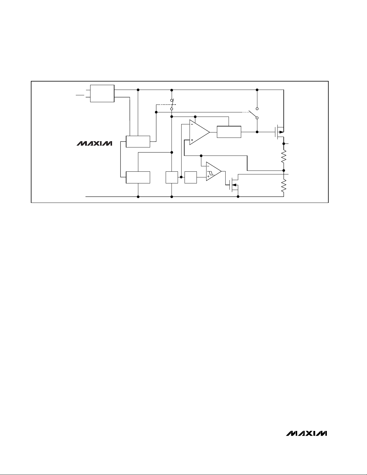
_______________Detailed Description
The MAX8875 is a low-dropout, low-quiescent-current
linear regulator designed primarily for battery-powered
applications. The device supplies loads up to 150mA
and is available with preset output voltages of 2.5V,
2.7V, 3.0V, 3.3V, or 5.0V. As illustrated in Figure 1, the
MAX8875 consists of a 1.25V reference, error amplifier,
P-channel pass transistor, power-OK comparator, and
internal feedback voltage divider.
The 1.25V bandgap reference is connected to the error
amplifier’s inverting input. The error amplifier compares
this reference with the feedback voltage and amplifies
the difference. If the feedback voltage is lower than the
reference voltage, the pass-transistor gate is pulled
lower, which allows more current to pass to the output
and increases the output voltage. If the feedback voltage is too high, the pass-transistor gate is pulled up,
allowing less current to pass to the output. The output
voltage feeds back through an internal resistor voltage
divider connected to the OUT pin.
Additional blocks include a current limiter, reversebattery protection, thermal sensor, and shutdown logic.
Output Voltage
The MAX8875 is supplied with factory-set output voltages of 2.5V, 2.7V, 3.0V, 3.3V, or 5.0V. The part number’s
two-digit suffix identifies the nominal output voltage. For
example, the MAX8875EUK33 has a preset output voltage of 3.3V (see Output Voltage Selector Guide).
Internal P-Channel Pass Transistor
The MAX8875 features a 1.1Ω (typ) P-channel MOSFET
pass transistor. This provides several advantages over
similar designs using PNP pass transistors, including
longer battery life. The P-channel MOSFET requires no
base drive, which reduces quiescent current significantly. PNP-based regulators waste considerable
current in dropout when the pass transistor saturates.
They also use high base-drive currents under large
loads. The MAX8875 does not suffer from these problems and consumes only 100µA of quiescent current
whether in dropout, light-load, or heavy-load applications (see Typical Operating Characteristics).
Power-OK Output
When the output voltage goes out of regulation—as during dropout, current limit, or thermal shutdown—POK
goes low. POK is an open-drain N-channel MOSFET. To
obtain a logic-level output, connect a pull-up resistor
from POK to OUT. To minimize current consumption,
make this resistor as large as practical. A 100kΩ resistor
works well for most applications. A capacitor to GND
may be added to generate a power-on-reset (POR)
delay. The POK function is not active during shutdown.
POK also provides a power-on-reset function that can
operate down to VIN≤ 1V. See POK Startup Response
in the Typical Operating Characteristics.
MAX8875
150mA, Low-Dropout Linear Regulator
with Power-OK Output
6 _______________________________________________________________________________________
Figure 1. Functional Diagram
REVERSE-
IN
SHDN
BATTERY
PROTECTION
SHUTDOWN
MAX8875
GND
LOGIC
THERMAL
SENSOR
1.25V
REF
P
OUT
POK
95%
REF
ERROR
AMP
POK
MOS DRIVER
WITH I
LIMIT
Page 7

Current Limit
The MAX8875 includes a current limiter that monitors
and controls the pass transistor’s gate voltage, limiting
the output current to 390mA (typ). For design purposes, consider the current limit to be 160mA min to
600mA max. The output can be shorted to ground for
an indefinite period of time without damaging the part.
Thermal-Overload Protection
When the junction temperature exceeds TJ= +170°C,
the thermal sensor signals the shutdown logic, turning
off the pass transistor and allowing the IC to cool. The
thermal sensor will turn the pass transistor on again after
the IC’s junction temperature cools by 20°C, resulting in
a pulsed output during continuous thermal-overload
conditions.Thermal-overload protection is designed to
protect the MAX8875 in the event of fault conditions. For
continuous operation, do not exceed the absolute maximum junction-temperature rating of TJ= +150°C.
Operating Region and Power Dissipation
The MAX8875’s maximum power dissipation depends
on the thermal resistance of the case and circuit board,
the temperature difference between the die junction
and ambient air, and the rate of air flow. The power dissipation across the device is P = I
OUT(VIN
- V
OUT
). The
maximum power dissipation is:
P
MAX
= (TJ- TA) / (θJB+ θBA)
where T
J
- TAis the temperature difference between
the MAX8875 die junction and the surrounding air, θ
JB
(or θJC) is the thermal resistance of the package, and
θ
BA
is the thermal resistance through the printed circuit
board, copper traces, and other materials to the surrounding air.
The MAX8875’s ground pin (GND) performs the dual
function of providing an electrical connection to system
ground and channeling heat away. Connect GND to the
system ground using a large pad or ground plane.
Reverse-Battery Protection
The MAX8875 has a unique protection scheme that limits the reverse supply current to 1mA when either VINor
V
SHDN
falls below ground. The circuitry monitors the
polarity of these two pins and disconnects the internal
circuitry and parasitic diodes when the battery is
reversed. This feature prevents device damage.
__________Applications Information
Capacitor Selection and
Regulator Stability
For stable operation over the full temperature range
and with load currents up to 150mA, use a 1µF (min)
ceramic output capacitor with an ESR <0.2Ω. To
reduce noise and improve load-transient response, stability, and power-supply rejection, use large output
capacitor values, such as 10µF.
Note that some ceramic dielectrics exhibit large capacitance and ESR variation with temperature. With
dielectrics such as Z5U and Y5V, it may be necessary
to use 2.2µF or more to ensure stability at temperatures
below TA= -10°C. With X7R or X5R dielectrics, 1µF
should be sufficient at all operating temperatures. Also,
for high-ESR tantalum capacitors, 2.2µF or more and a
larger case size may be needed to maintain ESR in the
stable region. For a pin-compatible, functionally equivalent device for use with a higher ESR output capacitor,
see the MAX8885. A graph of the Region of Stable
C
OUT
ESR vs. Load Current is shown in the Typical
Operating Characteristics.
PSRR and Operation from
Sources Other than Batteries
The MAX8875 is designed to deliver low dropout voltages
and low quiescent currents in battery-powered systems.
Power-supply rejection is 60dB at low frequencies. See
the Power-Supply Rejection Ratio vs. Frequency graph in
the Typical Operating Characteristics.
Improve supply-noise rejection and transient response
by increasing the values of the input and output bypass
capacitors. The Typical Operating Characteristics show
the MAX8875’s line- and load-transient responses.
Dropout Voltage
A regulator’s minimum input-output voltage differential
(or dropout voltage) determines the lowest usable supply
voltage. In battery-powered systems, this will determine
the useful end-of-life battery voltage. Because the
MAX8875 uses a P-channel MOSFET pass transistor,
its dropout voltage is a function of drain-to-source
on-resistance (R
DS(ON)
) multiplied by the load current
(see Typical Operating Characteristics):
V
DROPOUT
= VIN- V
OUT
= R
DS(ON)
· I
OUT
MAX8875
150mA, Low-Dropout Linear Regulator
with Power-OK Output
_______________________________________________________________________________________ 7
Chip Information
TRANSISTOR COUNT: 266
Page 8

MAX8875
150mA, Low-Dropout Linear Regulator
with Power-OK Output
Maxim cannot assume responsibility for use of any circuitry other than circuitry entirely embodied in a Maxim product. No circuit patent licenses are
implied. Maxim reserves the right to change the circuitry and specifications without notice at any time.
8 _____________________Maxim Integrated Products, 120 San Gabriel Drive, Sunnyvale, CA 94086 408-737-7600
© 1999 Maxim Integrated Products Printed USA is a registered trademark of Maxim Integrated Products.
Package Information
SOT5L.EPS
 Loading...