

Datasheet MAX8866TEUA, MAX8865REUA, MAX8865SEUA, MAX8865TEUA, MAX8866REUA Datasheet (Maxim)
...Page 1
19-0485; Rev 0; 4/96
Dual, Low-Dropout, 100mA Linear Regulators
_______________General Description
The MAX8865 and MAX8866 dual, low-dropout linear
regulators operate from a +2.5V to +5.5V input range
and deliver up to 100mA. At 200mA total load, the
PMOS pass transistors keep the supply current at
145µA, making these devices ideal for battery-operated
portable equipment such as cellular phones, cordless
phones, and modems.
The devices feature Dual Mode™ operation: their output voltages are preset (at 3.15V for the “T” versions,
2.84V for the “S” versions, or 2.80V for the “R” versions)
or can be adjusted with external resistor dividers. Other
features include independent low-power shutdown,
short-circuit protection, thermal shutdown protection,
and reverse battery protection. The MAX8866 also
includes an auto-discharge function, which actively discharges the selected output voltage to ground when
the device is placed in shutdown mode. Both devices
come in a miniature 8-pin µMAX package.
________________________Applications
Cordless Telephones Modems
PCS Telephones Hand-Held Instruments
Cellular Telephones Palmtop Computers
PCMCIA Cards Electronic Planners
____________________________Features
♦ Low Cost
♦ Low, 55mV Dropout Voltage @ 50mA I
OUT
♦ Low, 105µA No-Load Supply Current
♦ Low, 145µA Operating Supply Current (even in
dropout)
♦ Low, 350µV
Output Noise
RMS
♦ Independent, Low-Current Shutdown Control
♦ Thermal Overload Protection
♦ Output Current Limit
♦ Reverse Battery Protection
♦ Dual Mode Operation: Fixed or Adjustable (1.25V
to 5.5V) Outputs
______________Ordering Information
PART
MAX8865TEUA
MAX8865SEUA
MAX8865REUA -40°C to +85°C 8 µMAX 2.80
MAX8866TEUA
MAX8866SEUA -40°C to +85°C 8 µMAX 2.84
MAX8866REUA -40°C to +85°C 8 µMAX 2.80
TEMP. RANGE
-40°C to +85°C
-40°C to +85°C
-40°C to +85°C
PIN-
PACKAGE
8 µMAX
8 µMAX
8 µMAX
PRESET
V
(V)
OUT
3.15
2.84
3.15
MAX8865T/S/R, MAX8866T/S/R
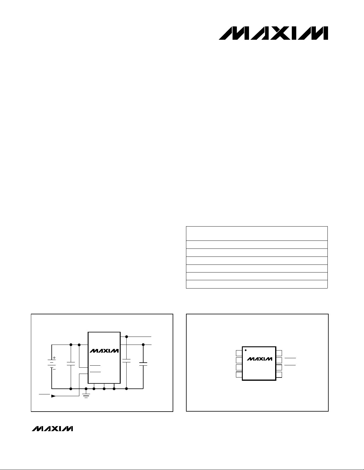
__________Typical Operating Circuit
OUTPUT
VOLTAGE 1
OUTPUT
VOLTAGE 2
C
OUT2
1µF
OUT1
MAX8865
MAX8866
OUT2
C
1µF
OUT1
IN
C
IN
BATTERY
SHDN2
Dual Mode is a trademark of Maxim Integrated Products.
2µF
SHDN1
SHDN2
GND SET2SET1
________________________________________________________________
__________________Pin Configuration
TOP VIEW
OUT1
GND
OUT2
1
2
IN
MAX8865
3
MAX8866
4
µMAX
Maxim Integrated Products
8
SET1
SHDN1
7
SHDN2
6
5
SET2
1
For free samples & the latest literature: http://www.maxim-ic.com, or phone 1-800-998-8800
Page 2
Dual, Low-Dropout, 100mA Linear Regulators
ABSOLUTE MAXIMUM RATINGS
VINto GND ..................................................................-6V to +6V
Output Short-Circuit Duration ............................................Infinite
SET_ to GND ............................................................-0.3V to +6V
SHDN_ _ to GND............................................................-6V to +6V
SHDN_ _ to IN .............................................................-6V to +0.3V
OUT_ to GND...............................................-0.3V to (V
Continuous Power Dissipation (T
= +70°C)
A
+ 0.3V)
IN
µMAX (derate 4.1mW/°C above +70°C)......................330mW
Stresses beyond those listed under “Absolute Maximum Ratings” may cause permanent damage to the device. These are stress ratings only, and functional
operation of the device at these or any other conditions beyond those indicated in the operational sections of the specifications is not implied. Exposure to
absolute maximum rating conditions for extended periods may affect device reliability.
ELECTRICAL CHARACTERISTICS
(VIN= +3.6V, GND = 0V, TA= 0°C to +85°C, unless otherwise noted. Typical values are at TA= +25°C.)
Operating Temperature Range ...........................-40°C to +85°C
Junction Temperature......................................................+150°C
Thermal Resistance (θ
)...............................................244°C/W
JA
Storage Temperature Range.............................-65°C to +160°C
Lead Temperature (soldering, 10sec).............................+300°C
CONDITIONS
Input Voltage (Note 1)
Output Voltage
Adjustable Output Voltage
Range (Note 2)
Current Limit (Note 3)
Ground Pin Current
Dropout Voltage (Note 4)
MAX8865T/S/R, MAX8866T/S/R
Line Regulation
Load Regulation
Output Voltage Noise
V
∆V
IN
OUT_
OUT_
LIM
Q
LNR
LDR
0mA ≤ I
OUT
SET_ = GND
SET_ = GND µAI
I
= 1mA
OUT
I
= 50mA
OUT
≤ 50mA,
MAX886_T
MAX886_S 2.77 2.84 2.91
MAX886_R
I
= 0mA
OUT_
I
= 50mA
OUT_
3.08 3.15 3.24
2.73 2.80 2.87
SET_
105 270
145
1.1
55 120
VIN= 2.5V to 5.5V, SET_ tied to OUT_,
I
= 1mA
OUT_
I
= 0mA to 50mA %/mA
OUT_
10Hz to 1MHz
SET_ = GND
SET_ tied to OUT_
C
= 1µF
OUT
C
= 100µF
OUT
0.012 0.03
0.006
350
220
SHUTDOWN
SHDN Input Threshold
SHDN Input Bias Current
Shutdown Supply Current V
IH
IL
SHDN_ _
Q SHDN
Shutdown to Output
Discharge Delay (MAX8866)
V
SHDN_ _
OUT_
C
= 1µF, no load
OUT
= V
= 0V
IN
2.0V
0 1000I
0.16 3000 nAI
SET INPUT
1.222 1.25 1.276V
0.015 50I
SET Input Leakage Current
(Note 2)
SET_
SET_
VIN= 2.5V to 5.5V, I
V
= 1.3V
SET_
= 1mASET Reference Voltage (Note 2) V
OUT_
THERMAL PROTECTION
Thermal Shutdown Temperature °C
Thermal Shutdown Hysteresis °C
SHDN
SHDN
170T
20∆T
UNITSMIN TYP MAXSYMBOLPARAMETER
V2.5 5.5V
V
5.5V
VV
mA100Maximum Output Current
mA220I
mV
%/V-0.10 0 0.10∆V
µV
RMS
0.4V
V
nA
ms1
nA
2 _______________________________________________________________________________________
Page 3
Dual, Low-Dropout, 100mA Linear Regulators
ELECTRICAL CHARACTERISTICS
(VIN= +3.6V, GND = 0V, TA= -40°C to +85°C, unless otherwise noted. Typical values are at TA= +25°C.) (Note 5)
CONDITIONS
Input Voltage (Note 1)
Output Voltage
Adjustable Output Voltage
Range (Note 2)
Current Limit (Note 3)
Ground Pin Current
Dropout Voltage (Note 4)
Line Regulation
Load Regulation
Output Voltage Noise
SHUTDOWN
SHDN Input Threshold
SHDN Input Bias Current
Shutdown Supply Current
Shutdown to Output
Discharge Delay (MAX8866)
SET INPUT
SET Input Leakage Current
(Note 2)
THERMAL PROTECTION
Thermal Shutdown Temperature °C
Thermal Shutdown Hysteresis °C
Note 1: Guaranteed by line regulation test.
Note 2: Adjustable mode only.
Note 3: Not tested. For design purposes, the current limit should be considered 120mA minimum to 320mA maximum.
Note 4: The dropout voltage is defined as (V
Note 5: Specifications to -40°C are guaranteed by design and not production tested.
IN
V
OUT_
OUT_
I
LIM
Q
LNR
∆V
LDR
IH
IL
I
SHDN_ _
Q SHDN
V
SET_
I
SET_
SHDN
∆T
SHDN
0mA ≤ I
OUT
≤ 50mA,
SET_ = GND
SET_ = GNDI
I
= 1mA
OUT
I
= 50mA
OUT
VIN= 2.5V to 5.5V,
SET_ tied to OUT_, I
I
= 0mA to 50mA
OUT_
10Hz to 1MHz
V
V
C
SHDN_ _
OUT_
OUT
= V
= 0V
= 1µF
IN
VIN= 2.5V to 5.5V, I
V
= 1.3V
SET_
- V
OUT_
) when V
IN_
MAX886_T
MAX886_S 2.74 2.84 2.93
MAX886_R
I
= 0mA
OUT_
I
= 50mA
OUT_
= 1mA
OUT_
SET_ = GND
SET_ tied to OUT_
C
= 1µF
OUT
C
= 100µF
OUT
= 1mASET Reference Voltage (Note 2)
OUT_
is 100mV below the value of V
OUT_
3.05 3.15 3.26
2.70 2.80 2.89
SET_
5.5V
220
105 270
145
1.1
55 120
0.012 0.03
0.006
350
220
2.0V
0.4V
0 1000
0.16 3000
1.207 1.25 1.288
0.015 50
170T
20
OUT_
for V
IN_
= V
OUT_
+2V.
UNITSMIN TYP MAXSYMBOLPARAMETER
V2.5 5.5V
V
VV
mA80Maximum Output Current
mA
µA
mV
%/V-0.11 0 0.11∆V
%/mA
µV
RMS
V
nA
nAI
ms1
V
nA
MAX8865T/S/R, MAX8866T/S/R
_______________________________________________________________________________________
3
Page 4
Dual, Low-Dropout, 100mA Linear Regulators
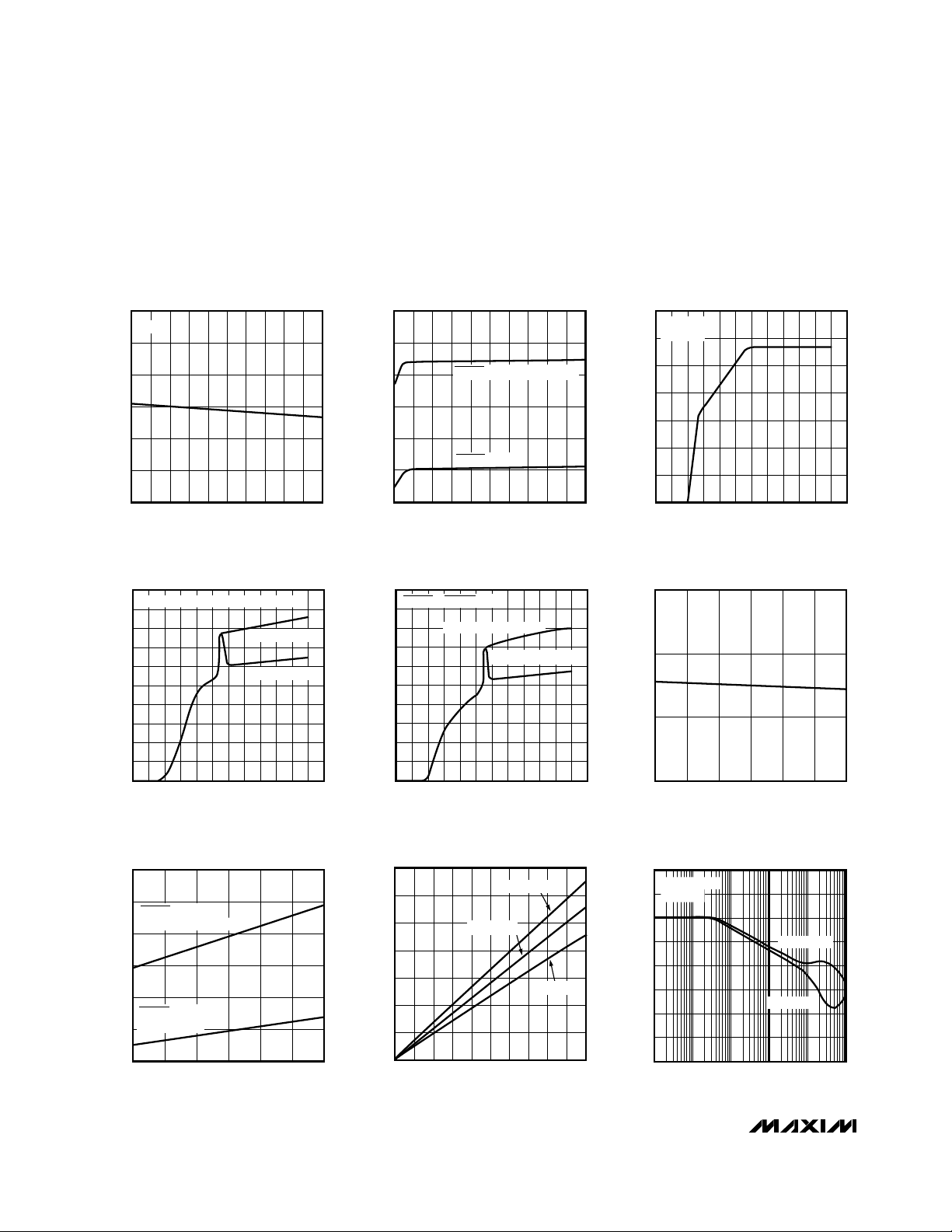
__________________________________________Typical Operating Characteristics
(V
= +3.6V, CIN= 2µF, C
IN
= 1µF, SHDN2 = GND, MAX886_S, TA= +25°C, unless otherwise noted.)
OUT
OUTPUT VOLTAGE
vs. LOAD CURRENT
3.00
V
OUT1
2.95
2.90
2.85
2.80
OUTPUT VOLTAGE (V)
2.75
2.70
0203010 60 70 100
40 50 80 90
LOAD CURRENT (mA)
MAX8865/66-01
180
160
140
120
100
SUPPLY CURRENT (µA)
80
60
02010 60 70 100
SUPPLY CURRENT
vs. INPUT VOLTAGE
MAX8865/66-04
200
180
160
140
120
100
80
60
SUPPLY CURRENT (µA)
40
20
0
01 4 6
100
ONE REGULATOR ENABLED, NO LOAD
90
80
70
60
MAX8865T/S/R, MAX8866T/S/R
50
40
30
SUPPLY CURRENT (µA)
20
10
0
01 4 6
23 5
INPUT VOLTAGE (V)
I
LOAD1 =
I
LOAD1
50mA
= 0mA
SUPPLY CURRENT
vs. LOAD CURRENT
SHDN2 = VIN, I
SHDN2 = GND
30 40 50 80 90
LOAD CURRENT (mA)
TOTAL SUPPLY CURRENT
vs. INPUT VOLTAGE
SHDN1 = SHDN2 = V
I
IN
= I
LOAD1
LOAD2 =
I
23 5
INPUT VOLTAGE (V)
LOAD1
LOAD2
50mA
= I
LOAD2
= 50mA
= 0mA
3.5
3.0
MAX8865/66-02
2.5
2.0
1.5
OUTPUT VOLTAGE (V)
1.0
0.5
0
3.0
MAX8865/66-05
2.9
2.8
OUTPUT VOLTAGE (V)
2.7
-40 -20 40 80
OUTPUT VOLTAGE
vs. INPUT VOLTAGE
V
OUT1
NO LOAD
01 4 6
23 5
INPUT VOLTAGE (V)
MAX8865/66-03
OUTPUT VOLTAGE
vs. TEMPERATURE
MAX8865/66-06
020 60
TEMPERATURE (°C)
SUPPLY CURRENT
vs. TEMPERATURE
180
160
SHDN2 = V
I
140
120
100
SUPPLY CURRENT (µA)
SHDN2 = GND
I
80
60
-40 -20 40 80
LOAD1
LOAD1
= I
= 50mA
IN
= 50mA
LOAD2
020 60
TEMPERATURE (°C)
140
120
MAX8865/66-07
100
80
60
40
DROPOUT VOLTAGE (mV)
20
0
0 20 60 100
DROPOUT VOLTAGE
vs. LOAD CURRENT
TA = +85°C
TA = +25°C
40 8010 30 7050 90
LOAD CURRENT (mA)
TA = -40°C
MAX8865/66-08
POWER-SUPPLY REJECTION RATIO
vs. FREQUENCY
80
V
= 2.84V
OUT
70
= 55Ω
R
L
60
50
40
PSRR (dB)
30
20
10
0
0.100.01
FREQUENCY (kHz)
4 _______________________________________________________________________________________
C
OUT
C
OUT
110
= 10µF
= 1µF
100 1000
MAX8865/66-09
Page 5

Dual, Low-Dropout, 100mA Linear Regulators
____________________________Typical Operating Characteristics (continued)
(V
= +3.6V, CIN= 2µF, C
IN
OUTPUT SPECTRAL NOISE DENSITY
10
RL = 55Ω
1
0.1
OUTPUT SPECTRAL NOISE DENSITY (µV/Hz)
0.01
0.1 10 1001 1000
= 1µF, SHDN2 = GND, MAX886_S, TA= +25°C, unless otherwise noted.)
OUT
vs. FREQUENCY
C
= 100µF
OUT
FREQUENCY (kHz)
C
= 1µF
OUT
MAX8865/66-10
1000
100
10
ESR (Ω)
OUT
1
C
0.1
0.01
0506070809010 20 30 40 100
OUTPUT NOISE DC TO 1MHz
REGION OF STABLE C
vs. LOAD CURRENT
C
= 1µF
OUT
INTERNAL FEEDBACK
EXTERNAL FEEDBACK
STABLE REGION
LOAD CURRENT (mA)
OUT
ESR
MAX8865/66-11
MAX8865T/S/R, MAX8866T/S/R
V
OUT
I
= 50mA, V
LOAD
LINE-TRANSIENT RESPONSE
4.6V
V
IN
3.6V
2.84V
2.83V
V
OUT
2.82V
50µs/div
I
LOAD
= 50mA, V
IS AC COUPLED
OUT
_______________________________________________________________________________________
IS AC COUPLED
OUT
1ms/div
I
LOAD
V
OUT
50mA
0mA
2.85V
2.84V
2.83V
VIN = 3.60V, I
LOAD-TRANSIENT RESPONSE
10µs/div
= 0mA to 50mA, CIN = 10µF, V
LOAD
IS AC COUPLED
OUT
5
Page 6

Dual, Low-Dropout, 100mA Linear Regulators
____________________________Typical Operating Characteristics (continued)
(V
= +3.6V, CIN= 2µF, C
IN
= 1µF, SHDN2 = GND, MAX886_S, TA= +25°C, unless otherwise noted.)
OUT
LOAD-TRANSIENT RESPONSE
I
LOAD
V
OUT
50mA
0mA
2.85V
2.84V
2.83V
V
= V
IN
OUT
V
IS AC COUPLED
OUT
+ 0.2V, I
10µs/div
= 0mA to 50mA, CIN = 10µF,
LOAD
I
LOAD
V
OUT
50mA
0mA
2.85V
2.84V
2.83V
CROSSTALK DUE TO LOAD TRANSIENT
V
OUT1
AC COUPLED
(10mV/div)
V
OUT2
AC COUPLED
MAX8865T/S/R, MAX8866T/S/R
(50mV/div)
= V
V
IN
OUT
V
IS AC COUPLED
OUT
LOAD-TRANSIENT RESPONSE
10µs/div
+ 0.1V, I
= 0mA to 50mA, CIN = 10µF,
LOAD
100mA
I
LOAD2
0mA
20µs/div
C
V
SHDN
V
OUT
2V
0V
4V
2V
0V
MAX8866 SHUTDOWN (NO LOAD)
500µs/div
NO LOAD
= 10µF, I
IN
= 100mA, SHDN2 = V
OUT1
IN
V
SHDN
V
OUT
MAX8866 SHUTDOWN (50mA LOAD)
2V
0V
4V
2V
0V
500µs/div
I
= 50mA
LOAD
6 _______________________________________________________________________________________
Page 7

Dual, Low-Dropout, 100mA Linear Regulators
______________________________________________________________Pin Description
PIN FUNCTIONNAME
OUT11
IN2 Regulator Input. Supply voltage can range from +2.5V to +5.5V. Bypass with 2µF to GND.
3 Ground. Solder to large pads or the circuit board ground plane to maximize thermal dissipation.
6
7
8
GND
OUT24
SET25
SHDN2
SHDN1
SET1
_______________Detailed Description
The MAX8865/MAX8866 are dual, low-dropout, low-quiescent-current linear regulators designed primarily for
battery-powered applications. They supply adjustable
1.25V to 5.5V outputs or preselected 2.80V
(MAX886_R), 2.84V (MAX886_S), or 3.15V (MAX886_T)
outputs for load currents up to 100mA. As illustrated in
Figure 1, these devices have a 1.25V reference and two
independent linear regulators. Each linear regulator
consists of an error amplifier, MOSFET driver, P-channel
pass transistor, Dual Mode™ comparator, and internal
feedback voltage divider.
The 1.25V bandgap reference is connected to the error
amplifiers’ inverting inputs. Each error amplifier compares this reference with the selected feedback voltage
and amplifies the difference. The MOSFET driver reads
the error signal and applies the appropriate drive to the
P-channel pass transistor. If the feedback voltage is
lower than the reference, the pass-transistor gate is
pulled lower, allowing more current to pass and
increasing the output voltage. If the feedback voltage is
too high, the pass-transistor gate is pulled up, allowing
less current to pass to the output.
The output voltage is fed back through either an internal resistor voltage divider connected to the OUT_ pin,
or an external resistor network connected to the SET_
pin. The Dual Mode comparator examines the SET_
Regulator 1 Output. Fixed or adjustable from 1.25V to 5.5V. Sources up to 100mA. Bypass with a 1µF
capacitor to GND.
Regulator 2 Output. Fixed or adjustable from 1.25V to 5.5V. Sources up to 100mA. Bypass with a 1µF
capacitor to GND.
Feedback Input for Setting the Output 2 Voltage. Connect to GND to set the output voltage to the preset 2.80V
(MAX886_R), 2.84V (MAX886_S), or 3.15V (MAX886_T). Connect to an external resistor divider for adjustableoutput operation.
Active-Low Shutdown 2 Input. A logic low turns off regulator 2. On the MAX8866, a logic low also causes the
output voltage to discharge to GND. Connect to IN for normal operation.
Active-Low Shutdown 1 Input. A logic low turns off regulator 1. On the MAX8866, a logic low also causes the
output voltage to discharge to GND. Connect to IN for normal operation.
Feedback Input for Setting the Output 1 Voltage. Connect to GND to set the output voltage to the preset 2.80V
(MAX886_R), 2.84V (MAX886_S), or 3.15V (MAX886_T). Connect to an external resistor divider for adjustableoutput operation.
voltage and selects the feedback path. If SET_ is below
60mV, internal feedback is used and the output voltage
is regulated to 2.80V for the MAX886_R, 2.84V for the
MAX886_S, or 3.15V for the MAX886_T. Both regulators
are preset for the same voltage. The reference and the
thermal sensor are shared between the regulators.
Duplicate blocks exist for current limiters, reverse battery protection, and shutdown logic.
Internal P-Channel Pass Transistor
The MAX8865/MAX8866 feature 1.1Ω typical P-channel
MOSFET pass transistors. This provides several advantages over similar designs using PNP pass transistors,
including longer battery life.
The P-channel MOSFET requires no base-drive current,
which reduces quiescent current significantly. PNPbased regulators waste considerable amounts of current in dropout when the pass transistor saturates. They
also use high base-drive currents under large loads.
The MAX8865/MAX8866 do not suffer from these problems, and consume only 145µA of quiescent current,
whether in dropout, light load, or heavy load applications (see
Typical Operating Characteristics
).
Output Voltage Selection
The MAX8865/MAX8866 feature Dual Mode operation:
they operate in either a preset voltage mode or an
adjustable mode.
MAX8865T/S/R, MAX8866T/S/R
_______________________________________________________________________________________ 7
Page 8

Dual, Low-Dropout, 100mA Linear Regulators
IN
SHDN1
REVERSE
BATTERY
PROTECTION
MAX8865
SHUTDOWN
LOGIC
ERROR
AMP
MAX8866
1.25V
REF
SHDN2
REVERSE
BATTERY
PROTECTION
THERMAL
SENSOR
MAX8865T/S/R, MAX8866T/S/R
MOS DRIVER
WITH I
DUAL-MODE
COMPARATOR
LIMIT
60mV
P
N
OUT1
*
SET1
MOS DRIVER
WITH I
DUAL-MODE
COMPARATOR
LIMIT
60mV
GND
* AUTO-DISCHARGE, MAX8866 ONLY
SHUTDOWN
LOGIC
ERROR
AMP
Figure 1. Functional Diagram
8 _______________________________________________________________________________________
P
N
OUT2
*
SET2
Page 9

Dual, Low-Dropout, 100mA Linear Regulators
OUTPUT
MAX8865
MAX8866
GND
OUT_
R1
SET_
R2
IN
C
IN
SHDN_
2µF
BATTERY
Figure 2. Adjustable Output Using External Feedback
Resistors
20pF
VOLTAGE
C
OUT
1µF
R
L
In preset voltage mode, internal, trimmed feedback
resistors set the MAX886_R outputs to 2.80V, the
MAX886_S outputs to 2.84V, and the MAX886_T outputs to 3.15V. Select this mode by connecting SET_ to
ground. If SET_ can’t be grounded in preset voltage
mode, limit impedances between SET_ and ground to
less than 100kΩ. Otherwise, spurious conditions could
cause the voltage at SET_ to exceed the 60mV Dual
Mode threshold.
In adjustable mode, select an output between 1.25V
and 5.5V using two external resistors connected as a
voltage divider to SET_ (Figure 2). The output voltage is
set by the following equation:
V
where V
= V
OUT_
= 1.25V. To simplify resistor selection:
SET_
R1 = R2
(1 + R1 / R2)
SET_
V
OUT
V
SET__
−
1
Choose R2 = 100kΩ to optimize power consumption,
accuracy, and high-frequency power-supply rejection.
The total current through the external resistive feedback
and load resistors should not be less than 10µA. Since
the V
tolerance is typically less than ±25mV, the
SET_
output can be set using fixed resistors instead of trim
pots. Connect a 10pF to 25pF capacitor across R1 to
compensate for layout-induced parasitic capacitances.
Shutdown
A low input on a SHDN_ _ pin individually shuts down one
of the two outputs. In shutdown mode, the selected
pass transistor, control circuit, and all biases are turned
off. When both sections are turned off, the reference
and thermal shutdown are also turned off and the supply current is typically reduced to 0.16nA. Connect
SHDN_ _ to IN for normal operation. The MAX8866 output
voltages are actively discharged to ground when individual regulators are shut down (see
Characteristics
).
Typical Operating
Current Limit
The MAX8865/MAX8866 include a current limiter for
each output section that monitors and controls the pass
transistor’s gate voltage, estimating the output current
and limiting it to about 220mA. For design purposes,
the current limit should be considered 120mA (min) to
320mA (max). The outputs can be shorted to ground for
an indefinite time period without damaging the part.
Thermal Overload Protection
Thermal overload protection limits total power dissipation in the MAX8865/MAX8866. When the junction temperature exceeds TJ= +170°C, the thermal sensor
sends a signal to the shutdown logic, turning off the
pass transistors and allowing the IC to cool. The thermal sensor will turn the pass transistors on again after
the IC’s junction temperature typically cools by 20°C,
resulting in a pulsed output during continuous thermal
overload conditions.
Thermal overload protection is designed to protect the
MAX8865/MAX8866 in the event of fault conditions.
Stressing the device with high load currents and high
input-output differential voltages (which result in elevated die temperatures above +125°C) may cause a
momentary overshoot (2% to 8% for 200ms) when the
load is completely removed. This can be remedied by
raising the minimum load current from 0µA (+125°C) to
100µA (+150°C). For continuous operation, do not
exceed the absolute maximum junction temperature
rating of TJ= +150°C.
Operating Region and Power Dissipation
Maximum power dissipation of the MAX8865/MAX8866
depends on the thermal resistance of the case and circuit board, the temperature difference between the die
junction and ambient air, and the rate of air flow. The
power dissipation across the device is P = I
V
). The resulting maximum power dissipation is:
OUT
P
= (TJ- TA) / θ
MAX
JA
where (TJ- TA) is the temperature difference between
the MAX8865/MAX8866 die junction and the surrounding air, and θJAis the thermal resistance of the package to the surrounding air (244°C/W).
OUT(VIN
MAX8865T/S/R, MAX8866T/S/R
-
_______________________________________________________________________________________ 9
Page 10

Dual, Low-Dropout, 100mA Linear Regulators
Reverse Battery Protection
The MAX8865/MAX8866 have a unique protection
scheme that limits the reverse supply current to less
than 1mA when either VINor V
ground. The circuitry monitors the polarity of these
pins, disconnecting the internal circuitry and parasitic
diodes when the battery is reversed. This feature prevents the device from overheating and damaging the
battery.
SHDN_ _
falls below
__________Applications Information
Capacitor Selection and
Regulator Stability
Normally, use two 1µF surface-mount ceramic capacitors on the input and a 1µF surface-mount ceramic
capacitor on each output of the MAX8865/MAX8866.
Larger input capacitor values and lower ESR provide
better supply-noise rejection and transient response. A
higher-value input capacitor (10µF) may be necessary
if large, fast transients are anticipated and the device is
located several inches from the power source. Improve
load-transient response, stability, and power-supply
rejection by using large output capacitors. For stable
operation over the full temperature range, with load currents of 100mA, a minimum of 1µF is recommended
(see the Region of Stable C
graph in the
MAX8865T/S/R, MAX8866T/S/R
The MAX8865/MAX8866 exhibit 350µV
normal operation. When using the MAX8865/MAX8866
in applications that include analog-to-digital converters
of greater than 12 bits, consider the ADC’s power-supply rejection specifications (see the Output Noise DC to
1MHz photo in the
Typical Operating Characteristics
Typical Operating Characteristics
Power-Supply Rejection and Operation
ESR vs. Load Current
OUT
noise during
RMS
).
Noise
).
(see the Power-Supply Rejection Ratio vs. Frequency
graph in the
When operating from sources other than batteries,
improve supply-noise rejection and transient response
by increasing the values of the input and output capacitors, and using passive filtering techniques (see the
supply and load-transient responses in the
Operating Characteristics
The MAX8865/MAX8866 load-transient response
graphs (see
two components of the output response: a DC shift of
the output voltage due to the different load currents,
and the transient response. Typical overshoot for step
changes in the load current from 0mA to 50mA is
12mV. Increasing the output capacitor’s value and
decreasing its ESR attenuates transient spikes.
Cross-regulation refers to the change in one output
voltage when the load changes on the other output. For
the MAX8865/MAX8866, cross-regulation for a 0mA to
50mA load change on one side results in less than 1mV
change of output voltage. If the power dissipation on
one output causes the junction temperature to exceed
125°C, ensure regulation of the other output with a minimum load current of 100µA.
A regulator’s minimum input-output voltage differential (or
dropout voltage) determines the lowest usable supply voltage. In battery-powered systems, this will determine the
useful end-of-life battery voltage. Because the
MAX8865/MAX8866 use P-channel MOSFET pass transistors, their dropout voltages are a function of R
plied by the load currents (see
from Sources Other than Batteries
The MAX8865/MAX8866 are designed to deliver low
dropout voltages and low quiescent currents in batterypowered systems. Power-supply rejection is 60dB at low
frequencies and rolls off above 400Hz. As the frequency
increases above 100kHz, the output capacitor is the
major contributor to the rejection of power-supply noise
___________________Chip Information
TRANSISTOR COUNT: 259
Typical Operating Characteristics
).
.
Typical
Load-Transient Considerations
Typical Operating Characteristics
Cross-Regulation
Input-Output (Dropout) Voltage
Electrical Characteristics
DS(ON)
) show
multi-
).
10 ______________________________________________________________________________________
Page 11

Dual, Low-Dropout, 100mA Linear Regulators
________________________________________________________Package Information
DIM
C
A
0.101mm
e
A1B
E H
0.004 in
L
α
A1
8-PIN µMAX
MICROMAX SMALL-OUTLINE
PACKAGE
D
INCHES MILLIMETERS
MIN
A
0.036
0.004
B
0.010
C
0.005
D
0.116
E
0.116
e
H
0.188
L
0.016
α
MAX
0.044
0.008
0.014
0.007
0.120
0.120
0°
0.198
0.026
6°
MIN
0.91
0.10
0.25
0.13
2.95
2.95
4.78
0.41
0°
MAX
1.11
0.20
0.36
0.18
3.05
3.05
0.650.0256
5.03
0.66
6°
21-0036D
MAX8865T/S/R, MAX8866T/S/R
______________________________________________________________________________________ 11
Page 12

Dual, Low-Dropout, 100mA Linear Regulators
MAX8865T/S/R, MAX8866T/S/R
Maxim cannot assume responsibility for use of any circuitry other than circuitry entirely embodied in a Maxim product. No circuit patent licenses are
Maxim cannot assume responsibility for use of any circuitry other than circuitry entirely embodied in a Maxim product. No circuit patent licenses are
implied. Maxim reserves the right to change the circuitry and specifications without notice at any time.
implied. Maxim reserves the right to change the circuitry and specifications without notice at any time.
12
__________________Maxim Integrated Products, 120 San Gabriel Drive, Sunnyvale, CA 94086 (408) 737-7600
12
__________________Maxim Integrated Products, 120 San Gabriel Drive, Sunnyvale, CA 94086 (408) 737-7600
© 1996 Maxim Integrated Products Printed USA is a registered trademark of Maxim Integrated Products.
© 1996 Maxim Integrated Products Printed USA is a registered trademark of Maxim Integrated Products.
 Loading...