

Page 1
19-1117; Rev 0; 8/96
Low-Cost, Low-Dropout, Dual Linear Regulator
_______________General Description
The MAX8862 low-cost, low-dropout, dual linear voltage
regulator is ideal for battery-powered and portable
applications. The regulators have independent supply
inputs and provide 250mA and 100mA, respectively,
with a full-load dropout voltage of 160mV. Both regulators use P-channel MOSFET pass transistors and maintain low quiescent current independent of load current.
In dropout, the MOSFET does not suffer from excessive
base currents, as do saturated PNP transistors.
The MAX8862 output voltage is preset to 4.95V (L),
3.175V (T), or 2.85V (R). This device employs Dual
Mode™ operation, allowing user-adjustable outputs
from +2V to +11V with external resistors. The input
supply-voltage range is 2.5V to 11.5V. Other features
include independent shutdown, power-good indicator,
short-circuit and reverse-battery protection, and thermal shutdown.
The MAX8862’s regulators are ideal power supplies for
the radio and the microcontroller (µC) used in digital,
cordless, and PCS phones. The main regulator is optimized for superior transient and dynamic response,
while the secondary regulator exhibits low-output, wideband noise.
The MAX8862 comes in a 16-pin SO package with a
lead frame that uses multiple GND pins as a heat sink
for additional thermal dissipation.
________________________Applications
Cellular Phones Cordless Phones
PCS Phones PCMCIA Cards
Modems Hand-Held Instruments
Electronic Planners
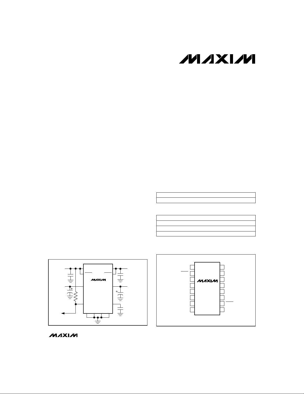
__________Typical Operating Circuit
INPUT 1
2.5V TO 11.5V
1µF
OUTPUT 1
AT 250mA
3.3µF
IN1
SHDN1 SHDN2
MAX8862
OUT1 OUT2
100k
PWROK1
GND SET1 SET2 GND
IN2
REF2
INPUT 2
2.5V TO 11.5V
1µF
OUTPUT 2
AT 100mA
2.2µF
0.1µF
____________________________Features
♦ Low Cost
♦ Guaranteed 250mA and 100mA Output Currents,
with Current Limiting
♦ Dual Mode Operation:
Fixed or Adjustable Output from +2V to +11V
♦ +2.5V to +11.5V Input Range
♦ 160mV Dropout Voltage at 200mA Output Current
♦ Low Supply Current—Even in Dropout
200µA Operating
<1µA Shutdown
♦ Power-Good Indicator
♦ Reverse-Battery Protection
♦ Thermal Overload Protection
______________Ordering Information
PART*
MAX8862_ESE -40°C to +85°C
*Insert the desired suffix letter (from the table below) into the
blank to complete the part number.
SUFFIX
L
T
R 2.85
TEMP. RANGE PIN-PACKAGE
16 Narrow SO
FIXED OUTPUT VOLTAGE (V)
4.95
3.175
__________________Pin Configuration
TOP VIEW
N.C.
16
SET1
15
14
OUT1
13
GND
GND
12
11
REF2
10
SHDN2
IN2
9
SHDN1
PWROK1
GND
GND
OUT2
SET2
N.C.
IN1
1
2
3
4
MAX8862
5
6
7
8
MAX8862
Narrow SO
Dual Mode is a trademark of Maxim Integrated Products.
________________________________________________________________
Maxim Integrated Products
1
For free samples & the latest literature: http://www.maxim-ic.com, or phone 1-800-998-8800
Page 2
Low-Cost, Low-Dropout, Dual Linear Regulator
ABSOLUTE MAXIMUM RATINGS
IN1, IN2 to GND (Note 1).....................................................±12V
SET1, SHDN1, PWROK1 to GND.............. -0.3V to (V
SET2, SHDN2, REF2 to GND....................... -0.3V, (V
Output Short-Circuit Duration ............................................Infinite
Continuous Power Dissipation (T
16-Pin Narrow SO (derate 20mW/°C above +70°C)............... 1W
= +70°C)
A
IN1
IN2
+ 0.3V)
+ 0.3V)
Note 1: Connect SHDN1 to IN1 and SHDN2 to IN2 through 20kΩ resistors to limit current flow in case a battery is reversed.
MAX8862
Stresses beyond those listed under “Absolute Maximum Ratings” may cause permanent damage to the device. These are stress ratings only, and functional
operation of the device at these or any other conditions beyond those indicated in the operational sections of the specifications is not implied. Exposure to
absolute maximum rating conditions for extended periods may affect device reliability.
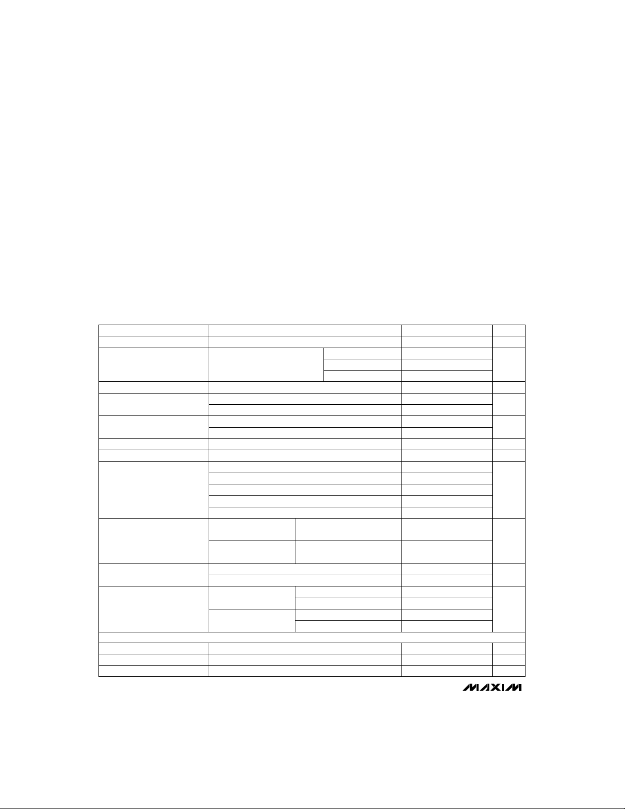
ELECTRICAL CHARACTERISTICS (Notes 2, 3)
(V
= V
IN_
OUT_(TYP)
Output Voltage
Maximum Output Current
Current Limit
Dropout Voltage (Note 4)
Line Regulation
Load Regulation
OUT2 Voltage Noise
REFERENCE
REF2 Output Voltage C
REF2 Line Regulation V
REF2 Load Regulation I
+ 1V, TA= 0°C to +85°C, unless otherwise noted. Typical values are at TA= +25°C.)
CONDITIONS
0mA < I
0mA < I
V
IN1
V
IN2
I
OUT1
I
OUT2
V
IN1
I
OUT1
I
OUT1
I
OUT2
I
OUT1
I
OUT2
I
OUT1
I
OUT1
I
OUT2
C
OUT2
Z
OUT2
C
OUT2
Z
OUT2
REF2
IN2
REF2
≤ 250mA,
OUT1
≤ 100mA
OUT2
= 2.5V min, V
= 2.5V min, V
= V
= 11.5V
IN2
= I
OUT2
OUT1
OUT2
= 1mA
= 2V
= 2V
= 200mA, MAX8862L/T
= 100mA, MAX8862L/T
= 200mA, MAX8862R
= 100mA, MAX8862R
= I
= 15mA
OUT2
= 0mA to 250mA, C
= 0mA to 100mA, C
= 2.2µF
= 10mA
= 100µF
= 10mA
= 0.1µF 1.230 1.250 1.270 V
= 2.5V to 11.5V 1 mV
= 0µA to 10µA 6 mV
Operating Temperature Range ...........................-40°C to +85°C
Junction Temperature .....................................................+150°C
Storage Temperature Range.............................-65°C to +150°C
Lead Temperature (soldering, 10sec)............................ +300°C
MAX8862L
MAX8862T
MAX8862R
4.80 4.95 5.15
3.050 3.175 3.300
2.75 2.85 2.95
250
100
580
250
1.5
160 330
160 350
165 350
180 400
V
= (V
IN1
OUT1 (TYP)
to 11.5V
V
= (V
IN2
OUT2 (TYP)
to 11.5V
= 3.3µF
OUT1
= 2.2µF
OUT2
10Hz < f < 100kHz
+ 1V)
+ 1V)
0.03 0.1
0.02 0.08
0.015
0.02
277
10Hz < f < 1MHz 875
10Hz < f < 100kHz
10Hz < f < 1MHz
211
667
UNITSMIN TYP MAXPARAMETER
%/mA
µVRMS
mV
V2.5 11.5Input Voltage Range
V
V211Output Voltage Range
mA
mA
µA200 330Quiescent Current
µA0.01 1Shutdown Supply Current
mV
%/V
RMS
2 _______________________________________________________________________________________
Page 3
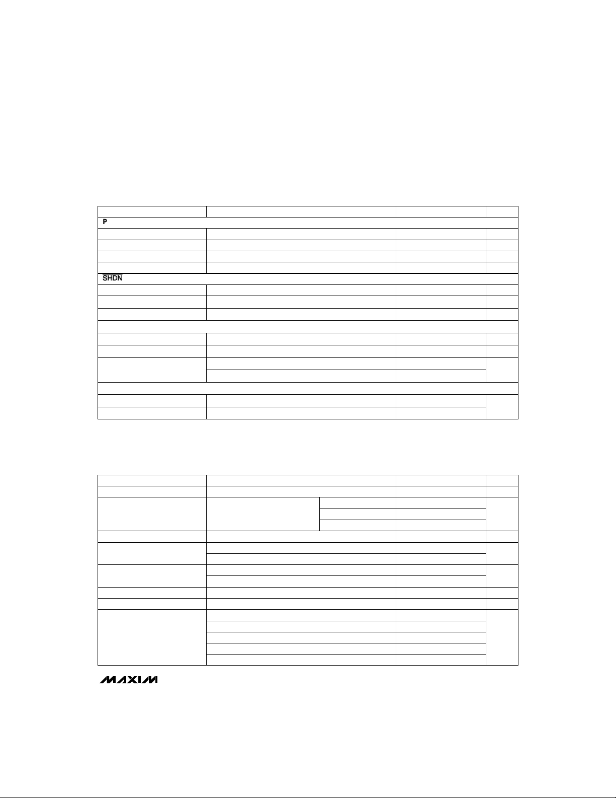
Low-Cost, Low-Dropout, Dual Linear Regulator
SHDN
ELECTRICAL CHARACTERISTICS (Notes 2, 3)
(V
IN_
= V
OUT_(TYP)
+ 1V, TA= 0°C to +85°C, unless otherwise noted. Typical values are at TA= +25°C.)
CONDITIONS
PWROK1 OUTPUT
Falling edge at SET1 V1.175 1.200 1.225PWROK1 Trip Voltage
Rising edge at SET1
PWROK1
SINK
SHDN_
= 11.5V
= 0.5mA
= 11.5V
IN_
= V
IN_
= 11.5V
OUT_(TYP)
SHDN_ Logic Low
SHDN_ Logic High
SHDN_ Leakage Current
V
I
Shutdown mode, V
Active mode, V
V
SET_ INPUT
SET_ Threshold
SET_ = OUT_, I
V
= 1.30V
SET_
Internal feedback
External feedback
OUT1
= I
OUT2
THERMAL PROTECTION
ELECTRICAL CHARACTERISTICS (Notes 2, 3)
(V
= V
IN_
OUT_(TYP)
Output Voltage
Maximum Output Current
Current Limit
Dropout Voltage (Note 4)
+ 1V, TA= -40°C to +85°C, unless otherwise noted. Typical values are at TA= +25°C.)
CONDITIONS
0mA < I
0mA < I
V
IN1
V
IN2
I
OUT1
I
OUT2
V
IN1
I
OUT1
I
OUT1
I
OUT2
I
OUT1
I
OUT2
≤ 250mA,
OUT1
≤ 100mA
OUT2
= 2.5V min, V
= 2.5V min, V
= V
= 11.5V
IN2
= I
OUT2
OUT1
OUT2
= 1mA
= 2V
= 2V
= 200mA, MAX8862L/T
= 100mA, MAX8862L/T
= 200mA, MAX8862R
= 100mA, MAX8862R
= 15mA
+ 1V to 11.5V
MAX8862L
MAX8862T
MAX8862R
40
250
160Thermal Shutdown Temperature
20Thermal Shutdown Hysteresis
4.80 4.95 5.15
3.050 3.175 3.300
2.740 2.85 2.960
250
100
580
250
1.5
160 330
160 350
165 350
180 400
MAX8862
UNITSMIN TYP MAXPARAMETER
mV15PWROK1 Hysteresis
µA0.01 1PWROK1 Leakage Current
mV25 200PWROK1 Low Voltage
V0.45
V1.8
µA0.01 1
V1.23 1.25 1.28SET_ Reference Voltage
µA0.01 0.1SET_ Input Bias Current
mV
°C
UNITSMIN TYP MAXPARAMETER
V2.5 11.5Input Voltage Range
V
V211Output Voltage Range
mA
mA
µA200 330Quiescent Current
µA0.01 1Shutdown Supply Current
mV
_______________________________________________________________________________________ 3
Page 4
Low-Cost, Low-Dropout, Dual Linear Regulator
SHDN
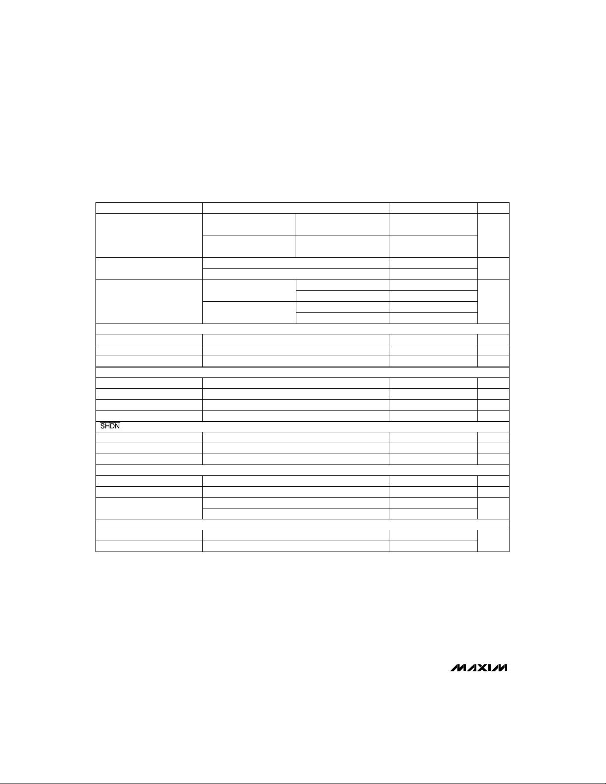
ELECTRICAL CHARACTERISTICS (Notes 2, 3) (continued)
(V
= V
IN_
OUT_(TYP)
Line Regulation
MAX8862
Load Regulation
OUT2 Voltage Noise
REFERENCE
REF2 Output Voltage C
REF2 Line Regulation V
REF2 Load Regulation
PWROK1 OUTPUT
PWROK1 Trip Voltage Falling edge at SET1 1.165 1.200 1.235 V
PWROK1 Hysteresis Rising edge at SET1 15 mV
PWROK1 Leakage Current V
PWROK1 Low Voltage I
+ 1V, TA= -40°C to +85°C, unless otherwise noted. Typical values are at TA= +25°C.)
CONDITIONS
V
= (V
IN1
I
= I
OUT1
I
OUT1
C
OUT2
C = 2.2µF, Z
C = 100µF, Z
REF2
= 2.5V to 11.5V 1 mV
IN2
I
REF2
PWROK1
SINK
= 15mA
OUT2
= 0 to 250mA, C
OUT1
= 3.3µF
= 2.2µF, 10Hz < f < 1MHz, I
= 10mA
OUT2
= 10mA
OUT2
= 0.1µF 1.217 1.250 1.277 V
= 0µA to 10µA 6 mV
= 11.5V 0.01 1 µA
= 0.5mA 25 200 mV
OUT1 (TYP)
to 11.5V
V
= (V
IN2
OUT2 (TYP)
to 11.5V
OUT2
10Hz < f < 100kHz
10Hz < f < 1MHz
10Hz < f < 100kHz
10Hz < f < 1MHz
+ 1V)
+ 1V)
= 10mA
- 277 -
- 875 -
- 211 -
- 667 -
0.03 0.12
0.02 0.10
0.015
0.02
UNITSMIN TYP MAXPARAMETER
%/V
%/mA
µV
RMS
SHDN_ Logic Low
SHDN_ Logic High
SHDN_ Leakage Current
= V
IN_
OUT_(TYP)
Active mode, V
V
= 11.5V 0.02 1 µA
SHDN_
= 11.5V 2.0 V
IN_
+ 1V to 11.5V
SET_ INPUT
SET_ Reference Voltage SET_ = OUT_, I
SET_ Input Bias Current V
SET_ Threshold
= 1.30V 0.01 0.1 µA
SET_
Internal feedback 30
External feedback 250
OUT1
= I
= 15mA 1.220 1.250 1.290 V
OUT2
THERMAL PROTECTION
Thermal Shutdown Temperature 160
Thermal Shutdown Hysteresis 10
Note 2: Guaranteed by design for TA= -40°C.
Note 3: Guaranteed for a junction temperature (T
design to operate up to T
Note 4: Dropout voltage is (VIN_ - V
the MAX8862 is tested by measuring the V
V
= 3.85V for the MAX8862R) then V
IN_
= +125°C. For TJabove +125°C, specifications exceed the operating limits.
J
_) when V
OUT
) equal to the operating temperature range. E-grade parts are guaranteed by
J
_ falls to 100mV below its nominal value at VIN_ = (V
OUT
_ at (V
OUT
is lowered until V
IN_
= 5.95V for the MAX8862L, V
IN_
falls 100mV below the measured value.
OUT_
= 4.175V for the MAX8862T, and
IN_
4 _______________________________________________________________________________________
0.45 VShutdown mode, V
_ + 1V). For example,
OUT
mV
°C
Page 5

Low-Cost, Low-Dropout, Dual Linear Regulator
__________________________________________Typical Operating Characteristics
(V
= V
-40
-40
IN2
-20
-20 20
= 5.3V, C
QUIESCENT CURRENT
vs. TEMPERATURE
V
IN1
04080
TEMPERATURE (°C)
OUTPUT VOLTAGE
vs. TEMPERATURE
TEMPERATURE (°C)
IN1
otherwise noted.)
260
240
220
200
180
160
140
QUIESCENT CURRENT (µA)
120
100
3.27
3.26
3.25
3.24
3.23
3.22
OUTPUT VOLTAGE (V)
3.21
3.20
= C
IN2
= 1µF, C
IN1
V
= V
= 12V
IN1
IN2
= V
= 7V
IN2
60
20
OUT1
OUT2
0
600
525
450
375
300
225
150
DROPOUT VOLTAGE (mV)
80 100
40
60
DROPOUT VOLTAGE
vs. LOAD CURRENT
75
0
0 80 200 320
40
LOAD CURRENT (mA)
_______________________________________________________________________________________
= 3.3µF, C
OUT1
120
MAX8862 TOC02
110
100
90
QUIESCENT CURRENT (µA)
80
0.001
100
MAX8862TOC06
OUT2
OUT1
120 280
160
0.01 0.1
101
100
99
98
97
96
NORMALIZED OUTPUT VOLTAGE (%)
95
0.001
0.01 0.1
240
= 2.2µF, SHDN1 = IN1, SHDN2 = IN2. TA= +25°C, unless
OUT2
QUIESCENT CURRENT
vs. LOAD CURRENT
I
I
10
1
LOAD CURRENT (mA)
OUTPUT VOLTAGE
vs. LOAD CURRENT
V
OUT1
V
OUT2
10
1
LOAD CURRENT (mA)
120
100
MAX8862 TOC03
Q2
Q1
100
100
80
60
40
SHUTDOWN CURRENT (nA)
20
1000
4
MAX8862TOC04
3
2
OUTPUT VOLTAGE (V)
1
0
1000
SHUTDOWN CURRENT
vs. TEMPERATURE
0
-20 0 20 40 60 80
-40
OUTPUT VOLTAGE & QUIESCENT CURRENT
2
TEMPERATURE (°C)
MAX8862T
vs. SUPPLY VOLTAGE
V
(IQ1 + IQ2)
35
4
6
SUPPLY VOLTAGE (V)
OUT1/VOUT2
OVERSHOOT AND TIME
EXITING SHUTDOWN MODE
MAX8862TOC07
A
0V
B
0V
= 5.3V, I
V
IN1
A = SHDN1, 0.8V TO 2.4V, 1V/div
B = OUT1, 1V/div
OUT1
20µs/div
= 5mA
V
= V
= 12V
IN1
IN2
V
= V
IN1
IN2
89101112
7
MAX8862TOC14
= 7V
1V/div
1V/div
MAX8862 TOC01
100
260
240
MAX8862TOC05
220
200
180
160
140
120
100
MAX8862
QUIESCENT CURRENT (µA)
5
Page 6

Low-Cost, Low-Dropout, Dual Linear Regulator
____________________________Typical Operating Characteristics (continued)
(V
= V
IN2
= 5.3V, C
IN1
otherwise noted.)
= C
IN2
= 1µF, C
IN1
OUT1 NOISE AND RIPPLE
OUT1
MAX8862TOC08
= 3.3µF, C
= 2.2µF, SHDN1 = IN1, SHDN2 = IN2. TA= +25°C, unless
OUT2
OUT2 NOISE AND RIPPLE
MAX8862TOC09
MAX8862
I
= 250mA, AC COUPLED
OUT1
OUT1 LOAD-TRANSIENT RESPONSE
A
B
= 7V, V
V
IN1
A = LOAD CURRENT, 0mA TO 300mA, 0.2A/div
B = V
= 3.2V
OUT1
RIPPLE, 50mV/div, AC COUPLED
OUT1
OUT2 LINE-TRANSIENT RESPONSE
5µs/div
2ms/div
V
OUT
500µV/div
V
OUT
1mV/div
5µs/div
= 100mA, AC COUPLED
I
MAX8862TOC10
300mA
0mA
OUT2
OUT2 LOAD-TRANSIENT RESPONSE
A
MAX8862TOC11
200mA
0mA
B
50mV/div
50mV/div
2ms/div
V
= 7V, V
= 3.2V
OUT2
RIPPLE, 50mV/div, AC COUPLED
OUT2
OUT1 LINE-TRANSIENT RESPONSE
MAX8862TOC13
MAX8862TOC12
IN2
A = LOAD CURRENT, 0mA TO 200mA, 0.2A/div
B = V
6.5V
A
B
5.5V
50mV/div
A
B
I
= 200mA, V
OUT2
A = V
B = V
OUT2
, 5.5V TO 6.5V, 1V/div
IN2
RIPPLE, 50mV/div, AC COUPLED
OUT2
1ms/div
= 3.2V
= 300mA, V
I
OUT1
= 5.5V TO 6.5V, 1V/div
A = V
IN1
RIPPLE, 50mV/div, AC COUPLED
B = V
OUT1
OUT1
1ms/div
= 3.2V
6 _______________________________________________________________________________________
6.5V
5.5V
50mV/div
Page 7

Low-Cost, Low-Dropout, Dual Linear Regulator
______________________________________________________________Pin Description
PIN
Main Regulator Supply Input (2.5V to 11.5V). Bypass with a 1µF, low-ESR capacitor to GND.IN11
2
10
11 REF2 Secondary Reference Output. Bypass with a 0.1µF capacitor to GND.
14 OUT1
15 SET1
SHDN1
PWROK13
OUT26
SET27
SHDN2
Main Regulator Shutdown Input. A logic low turns off the main regulator and power-good comparator.
Power-Good Output. This open-drain output is low when V
lower than its nominal value).
Ground. Connect to a ground plane to maximize thermal dissipation.GND4, 5, 12, 13
Secondary Regulator Output. Bypass with a 2.2µF low-ESR (< 0.5Ω) capacitor to GND. To improve
load-transient response and noise performance, use a higher-value, lower-ESR capacitor.
OUT2 Voltage-Set Input. Connect to GND for the factory-preset output voltage. Connect to a resistive
divider from OUT2 to GND for adjustable output voltage.
No connect. There is no internal connection to this pin.N.C. 8, 16
Secondary Regulator Supply Input (2.5V to 11.5V). Bypass with a 1µF, low-ESR capacitor to GND.IN29
Secondary Regulator Shutdown Input. A logic-low input turns off the secondary regulator and the
reference.
Main Regulator Output. Bypass with a 3.3µF, low-ESR (< 0.5Ω) capacitor to GND. To improve loadtransient response and noise performance, use a higher-value, lower-ESR capacitor.
OUT1 Voltage Set Input. Connect to GND for the factory-preset output voltage. Connect to a
resistive divider from OUT1 to GND for adjustable output voltage.
_______________Detailed Description
The MAX8862 features Dual Mode™ operation, allowing a fixed output of 4.95V (L), 3.175V (T), or 2.85V (R),
or an adjustable output from 2V to 11V. The regulator’s
outputs, OUT1 and OUT2, supply 250mA and 100mA,
respectively.
The block diagram (Figure 1) shows the contents of
each regulator. Note that the main regulator provides a
power-good indicator, and the secondary regulator’s
reference output voltage is available at REF2.
The 1.25V bandgap reference is connected to the error
amplifier’s inverting input. The error amplifier compares
this reference with the selected feedback voltage and
amplifies the difference. The MOSFET driver reads the
error signal and applies the appropriate drive to the
P-channel transistor. If the feedback voltage is lower
than the reference, the pass transistor’s gate is pulled
lower, allowing more current to pass and increase the
output voltage. If the feedback voltage is too high, the
pass transistor’s gate is pulled up, allowing less current
to pass to the output.
FUNCTIONNAME
is out of regulation (V
OUT1
OUT1
is 4%
The output voltage is fed back through either an
internal resistor voltage divider connected to OUT1/
OUT2, or an external resistor network connected to
SET1/SET2. The Dual Mode comparator examines
V
SET1/VSET2
and selects the feedback path. If this voltage is below 40mV, internal feedback is used and the
output voltage is regulated to the factory-preset voltage.
Internal P-Channel Pass Transistor
The MAX8862’s P-channel pass transistor provides
several advantages over similar designs using PNP
pass transistors, including longer battery life.
The P-channel MOSFET requires no continuous base
current, thereby reducing quiescent current considerably. PNP regulators normally waste a considerable
amount of current in dropout when the pass transistor
saturates; they also use high base-drive currents under
large loads. The MAX8862 does not suffer from these
problems: it consumes only 200µA of quiescent current
for both regulators under light and heavy loads, as well
as in dropout.
MAX8862
_______________________________________________________________________________________ 7
Page 8

Low-Cost, Low-Dropout, Dual Linear Regulator
1N1
SHDN1
MAX8862
IN2
SHDN2
REF2
BIAS
BIAS
1.25V
1.25V
OUT1
R1
50mV
G1
R2
R3
G1
R4
80mV
MAX8862
80mV
PWROK1
SET1
GND
GND
OUT
SET2
GND
GND
Figure 1. Functional Diagram
The MAX8862’s Dual Mode operation allows a fixed or
adjustable output voltage. In preset/internal-feedback
mode (SET1/SET2 = GND), output voltages are factory
preset to 4.95V (L), 3.175V (T), or 2.85V (R).
In adjustable/external feedback mode, output voltage is
adjusted between 2V and 11V with two external resistors connected as a voltage divider to SET1/SET2
(Figure 2). Since the input bias current at SET1/SET2 is
<0.1µA, large resistance values can be used for R1
and R2 to minimize power consumption without losing
accuracy. Select R2 in the 10kΩ to 400kΩ range. R1 is
given by:
R1 = R2 (V
where V
8 _______________________________________________________________________________________
SET
= 1.25V.
OUT
/ V
SET
- 1)
The MAX8862’s main regulator features a power-good
indicator that asserts when the output voltage falls out
of regulation. In internal-feedback mode, the opendrain PWROK1 output goes low when OUT1 falls 4%
below its nominal value. When used in external feedback mode, PWROK1 goes low when V
1.2V. A 100kΩ pull-up resistor from PWROK1 to V
provides a logic-control signal. This resistor also minimizes current flow to the input in case the battery is
reversed. PWROK1 can be used to reset a microcontroller or to drive an external LED for indicating a power
failure.
Output Voltage Selection
Power-Good Comparator
SET1
falls below
IN1
Page 9

Low-Cost, Low-Dropout, Dual Linear Regulator
MAX8862
GND
Figure 2. Adjustable Output Voltage
OUT_
SET_
OUTPUT
R1
R2
Reference
The MAX8862 provides a precision 1.25V reference at
REF2. Bypass REF2 with a 0.1µF capacitor to ground.
Larger bypassing capacitors will further reduce the
secondary regulator’s wideband noise.
Shutdown
The MAX8862’s regulators have individual shutdown
controls. A logic low on either SHDN1 or SHDN2 turns
off the corresponding internal reference, error comparator, and pass transistors’ control logic, reducing
quiescent current to less than 1µA.
Current Limiting
The MAX8862 features a current limit for each regulator. It monitors and controls the pass transistor’s gate
voltage, limiting the output current to 580mA for the
main regulator and 250mA for the secondary regulator.
The current limits apply to all input and output voltage
conditions. The outputs can be shorted to ground for
an indefinite period of time if the package can dissipate
(V
x I
+ V
x I
IN1
LIM1
+150°C (see the
Region
section).
IN2
Power Dissipation and Operating
) without exceeding TJ=
LIM2
Thermal overload protection limits the MAX8862’s total
Thermal Overload Protection
power dissipation. When the junction temperature
exceeds TJ= +160°C, the thermal sensor sends a signal to the shutdown logic, turning off the pass transistors and allowing the device to cool down. The thermal
sensor turns the pass transistors on again after the IC’s
junction temperature decreases by 20°C. If the thermal
overload condition persists, OUT1 and OUT2 pulse on
and off.
Thermal overload protection is designed to protect the
MAX8862 during fault conditions. For continuous operation, the absolute maximum junction temperature rating of TJ= +150°C should not be exceeded.
Reverse-Battery Protection
This feature protects the MAX8862 against polarity
reversal at the supply inputs. The inputs can handle
negative voltages up to -12V without suffering any ill
effects. When the input polarity is reversed, the output
will be at the same potential as ground, and no current
will flow from the output back to the input. This feature
protects both the device and the supply-voltage
source. The reverse currents that flow back to the input
are due to R
PWROK1
currents are approximately: I
R
PWROK1
) and I
ing the MAX8862 in continuous mode (V
and V
SHDN2
= V
, R
= |V
REV2
) place a resistor (>20kΩ) between
IN2
SHDN1
REV1
IN2
|
, and R
= |V
/ R
SHDN2
SHDN2
/ (R
IN1
|
. When operat-
SHDN1
. These
SHDN1
= V
IN1
shutdown and supply inputs to limit the current flow in
case the battery is reversed.
MAX8862
+
_______________________________________________________________________________________ 9
Page 10

Low-Cost, Low-Dropout, Dual Linear Regulator
pins to ground using a large pad or ground plane.
100
80
60
(°C/W)
BA
40
MAX8862
R0
20
0
0
510152025
PC-BOARD COPPER FOIL AREA (Cm
MAX8862 FIG03
35
30
2
)
Figure 3. Typical Copper Thermal Resistance vs. Copper
Ground Pad Area
400
350
300
)
250
OUT2
200
+ I
150
OUT1
(I
100
50
MAXIMUM OUTPUT CURRENT (mA)
0
2
(R)
345
(T)
MAXIMUM CURRENT
(R)
(L)
MAXIMUM
SUPPLY
VOLTAGE
OPERATING REGION AT
= +25°C, TJ = +125°C
T
A
6
7
SUPPLY VOLTAGE (V)
8 9 10 11
MAX8862FGIG04
(L)
(T)
12
Figure 4. Safe Operating Regions: Main and Secondary
Regulators Maximum Output Current vs. Supply Voltage
__________Applications Information
Power Dissipation and Operating Region
The MAX8862’s maximum power dissipation depends
on the thermal resistance of the case and circuit board,
the temperature difference between the die junction
and ambient air, and the rate of air flow.
The GND pins of the MAX8862 SO package perform
the dual function of providing an electrical connection
to ground and channeling heat away. Connect all GND
Where this is impossible, place a copper plane on an
adjacent layer. For a given power dissipation, the pad
should exceed the associated dimensions in Figure 3.
This figure shows a typical thermal resistance for a
35µm-thick copper foil as a function of its area
The power dissipation across the device is given by:
P = I
OUT1(VIN1
- V
OUT1
) + I
OUT2(VIN2
- V
The resulting power dissipation is as follows:
P = (TJ- TA) / (θJB+ θBA)
where (TJ- TA) is the temperature difference between
the MAX8862 die junction and the surrounding air, θ
(or θJC) is the thermal resistance of the package, and
θBAis the thermal resistance through the printed circuit
board, copper traces, and other materials to the surrounding air. The MAX8862’s narrow SO package has a
thermal resistance of θJB= +50°C/W.
The MAX8862 regulators deliver the rated output currents and operate with input voltages up to 11.5V, but
not simultaneously. High output currents can only be
sustained when input-output differential voltages are
small, as shown in Figure 4.
Capacitor Selection and
Regulator Stability
Filter capacitors are required at the MAX8862’s inputs
and outputs. 1µF ceramic capacitors are required at
the inputs. The minimum output capacitance required
for stability is 3.3µF for OUT1 and 2.2µF for OUT2. The
capacitor values depend primarily on the desired
power-up time and load-transient response. Loadtransient response is improved by using larger capacitor values. Input and output filter capacitors should be
soldered directly to pins to minimize lead inductance of
PC board traces.
The output capacitor’s equivalent series resistance
(ESR) affects stability and output noise. Surface-mount
ceramic capacitors have a very low ESR and are available up to 10µF. Otherwise, other low-ESR (<0.5Ω)
capacitors should be used. If the selected capacitor’s
ESR is higher than the recommended value, the capacitor value should be increased proportionally to maintain minimum output noise under all input voltage and
output load conditions. Paralleling two or more capacitors also results in lower ESR.
1
.
OUT2
).
JB
1
This graph was generated by Mr. Kieran O’Malley of Cherry Semiconductor Corp. and was published in the October 26, 1995, issue
of EDN magazine.
10 ______________________________________________________________________________________
Page 11

Low-Cost, Low-Dropout, Dual Linear Regulator
70
60
50
PSRR (dB)
40
30
20
0.01 1 100
A: I
OUT1
:
I
B
OUT1
C: I
OUT1
A
B
C
= 1mA
= 10mA
= 100mA
0.1
FREQUENCY (kHz)
OUT1
∆V
C
IN1
C
OUT1
IN1
= 1µF
10
= 1V
= 3.3µF
p-p
MAX8862FIG05A
70
65
60
55
50
45
PSRR (dB)
40
35
30
25
20
0.1
A: C
= 100µF
OUT1
B: C
= 10µF
OUT1
1 100
FREQUENCY (kHz)
OUT1
= 1V
IN1
OUT1
IN1
= 1µF
= 100mA
p-p
MAX8862FIG05B
1000
∆V
C
I
A
B
10
MAX8862
Figure 5a. Power-Supply Rejection Ratio vs. Ripple Frequency
for Light and Heavy Loads
Noise
The MAX8862’s OUT1 exhibits about 2.5mVp-p, and
OUT2 exhibits 1mVp-p of noise under full-load conditions. When using the MAX8862 for applications that
include analog-to-digital converters (ADCs) with resolutions greater than 12 bits, consider the ADC’s powersupply-rejection specifications.
PSRR and Operation
from Sources Other than Batteries
The MAX8862 is designed to achieve low dropout voltages and low quiescent currents in battery-powered
systems. However, to gain these benefits; the device
must trade away power-supply noise rejection, as well
as swift response to supply variations and load transients. For a 1mA load current, power-supply rejection
typically changes from 58dB to 43dB when the input
frequency is changed from 1Hz to 10kHz. At higher frequencies, the circuit depends primarily on the output
capacitor’s characteristics, and the PSRR increases
(Figure 5).
When operating from sources other than batteries, supply-noise rejection and transient response can be
improved by increasing the value of the input and output capacitors and employing passive filtering techniques. Do not use power supplies with ripple voltages
exceeding 200mV at 100kHz.
Figure 5b. Power-Supply Rejection Ratio vs. Ripple Frequency
for Various Output Capacitors
Overshoot and Transient Considerations
The
Typical Operating Characteristics
section shows
power-up, line, and load-transient response graphs.
Typical transients for step changes in the load current
from 0mA to 300mA are 100mVp-p. During recovery
from shutdown, overshoot is minimized by the 1µF
input, and output capacitors (3.3µF for OUT1, and
2.2µF for OUT2).
Input-Output (Dropout) Voltage
A regulator’s minimum input-to-output voltage differential (or dropout voltage) determines the lowest usable
supply voltage. In battery-powered systems, this determines the useful end-of-life battery voltage. Since
P-channel MOSFETs are used as pass transistors, the
dropout voltage is the product of the R
load current (see the
Electrical Characteristics
DS(ON)
and the
).
___________________Chip Information
TRANSISTOR COUNT: 457
______________________________________________________________________________________ 11
Page 12

Low-Cost, Low-Dropout, Dual Linear Regulator
________________________________________________________Package Information
INCHES MILLIMETERS
DIM
D
MAX8862
e
A
A1
DIM
D
D
D
B
C
E
e
H
L
PINS
A
0.101mm
0.004in.
A1
B
C
0°-8°
L
Narrow SO
HE
SMALL-OUTLINE
PACKAGE
(0.150 in.)
MAX
MIN
0.069
0.053
0.010
0.004
0.019
0.014
0.010
0.007
0.157
0.150
0.228
0.016
8
14
16
0.244
0.050
INCHES MILLIMETERS
MIN
MAX
0.189
0.197
0.337
0.344
0.386
0.394
MIN
1.35
0.10
0.35
0.19
3.80
5.80
0.40
MIN
4.80
8.55
9.80
1.270.050
MAX
1.75
0.25
0.49
0.25
4.00
6.20
1.27
MAX
5.00
8.75
10.00
21-0041A
Maxim cannot assume responsibility for use of any circuitry other than circuitry entirely embodied in a Maxim product. No circuit patent licenses are
Maxim cannot assume responsibility for use of any circuitry other than circuitry entirely embodied in a Maxim product. No circuit patent licenses are
Maxim cannot assume responsibility for use of any circuitry other than circuitry entirely embodied in a Maxim product. No circuit patent licenses are
Maxim cannot assume responsibility for use of any circuitry other than circuitry entirely embodied in a Maxim product. No circuit patent licenses are
implied. Maxim reserves the right to change the circuitry and specifications without notice at any time.
implied. Maxim reserves the right to change the circuitry and specifications without notice at any time.
implied. Maxim reserves the right to change the circuitry and specifications without notice at any time.
implied. Maxim reserves the right to change the circuitry and specifications without notice at any time.
12
__________________Maxim Integrated Products, 120 San Gabriel Drive, Sunnyvale, CA 94086 (408) 737-7600
12
__________________Maxim Integrated Products, 120 San Gabriel Drive, Sunnyvale, CA 94086 (408) 737-7600
12
__________________Maxim Integrated Products, 120 San Gabriel Drive, Sunnyvale, CA 94086 (408) 737-7600
12
__________________Maxim Integrated Products, 120 San Gabriel Drive, Sunnyvale, CA 94086 (408) 737-7600
© 1996 Maxim Integrated Products Printed USA is a registered trademark of Maxim Integrated Products.
© 1996 Maxim Integrated Products Printed USA is a registered trademark of Maxim Integrated Products.
© 1996 Maxim Integrated Products Printed USA is a registered trademark of Maxim Integrated Products.
© 1996 Maxim Integrated Products Printed USA is a registered trademark of Maxim Integrated Products.
 Loading...