

Page 1
General Description
The MAX8821 integrates a charge pump for white
LEDs, an audio loudspeaker amplifier, and two lownoise LDOs controlled by an I
2
C control interface. The
high-efficiency, adaptive-mode inverting charge pump
drives up to six LEDs with constant current for uniform
brightness. The LED current is controlled by an I
2
C
interface and adjusts from 0.1mA to 25.6mA per LED
into 32 pseudo-logarithmic steps. Independent voltages for each LED maximize efficiency even with large
LED forward voltage (V
F
) mismatch. An internal temperature derating function reduces the current above
+40°C to protect the LEDs.
The high-efficiency mono Class D audio amplifier delivers up to 2W into a 4Ω speaker from a 5V input supply.
The amplifier features proprietary filterless Active
Emissions Limiting (AEL) technology. AEL prevents
high-frequency emissions resulting from conventional
Class D free-wheeling behavior in the presence of an
inductive load. The amplifier offers two modulation
schemes: a fixed-frequency mode (FFM) and a spreadspectrum mode (SSM) that reduce EMI-radiated emissions due to the modulation frequency. The amplifier
also has robust output protection and high power-supply rejection ratio (PSRR). Click-and-pop suppression is
active during power-up/down, enable/disable, and for
all mode changes. The amplifier’s gain is adjustable
through an I2C interface, from -3dB to +24dB in 10 3dB
steps. Differential inputs improve common-mode noise
rejection.
The LDOs in the MAX8821 are designed for low-noise
operation. Each LDO output voltage can be individually
programmed by the I
2
C interface. Both LDO1 and
LDO2 have a high 70dB PSRR rating.
The MAX8821 includes soft-start, thermal shutdown,
open-circuit, and short-circuit protections, and is available in a compact 28-pin, Thin QFN, 4mm x 4mm package (0.8mm max height).
Applications
Cell Phones and Smartphones
PDAs, Digital Cameras, Camcorders
MP3 Players, GPS Devices
Features
♦ White LED Inverting Charge Pump
Independent Adaptive Current Regulators for
Each LED
6 Low-Dropout Current Regulators
Flexible I2C Dimming Control for Each LED
Ramp-Up/Down, Current Control for Each LED
Low 70µA (typ) Quiescent Current
TADerating Function Protects LEDs
♦ Mono 2W Class D Loudspeaker Amplifier
85% Efficiency (RL= 8Ω, P
OUT
= 600mW)
Low 0.05% THD+N at 1kHz
High 65dB PSRR at 1kHz
Fully Differential Inputs
-3dB to +24dB Gain Settings in 3dB Steps
Integrated Click-and-Pop Suppression
Low Quiescent Current
♦ Dual Low-Noise LDO
45µV
RMS
Output Noise, 70dB PSRR
Flexible I2C-Controlled Output Voltages
200mA and 300mA Output Current Drive
MAX8821
White LED Charge Pump with Mono Class D
Audio Amp and Dual LDO
________________________________________________________________
Maxim Integrated Products
1
19-1014; Rev 0; 10/07
For pricing, delivery, and ordering information, please contact Maxim Direct at 1-888-629-4642,
or visit Maxim's website at www.maxim-ic.com.
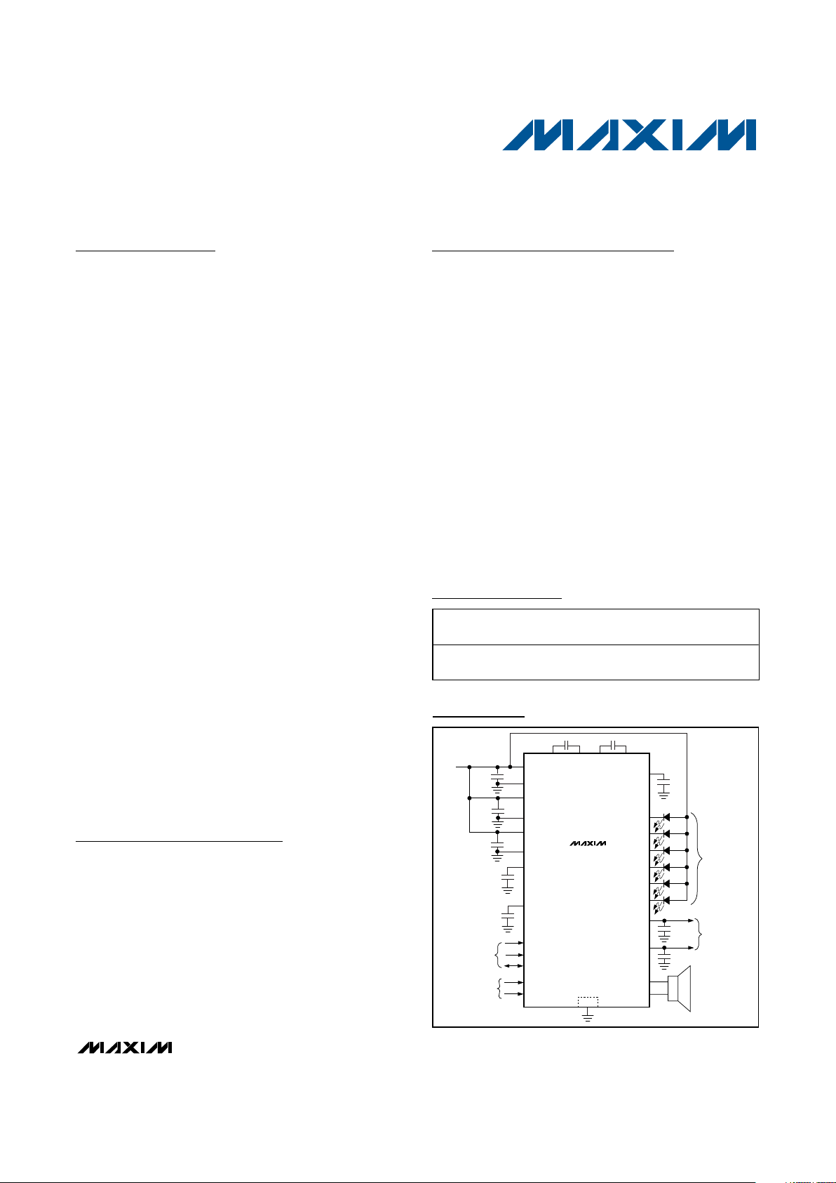
Ordering Information
NEG
LED1
LED5
LED4
LED3
LED2
LED6
DUAL LOW
NOISE LDO
LOUDSPEAKER/
EARPIECE
SPK+
SPK-
INDIVIDUAL
0.1mA TO
25.6mA
DIMMING
PGND1
IN1
CMREF
IN3
REF
AGND
IN2
PGND2
AIN+
AIN-
V
DD
SDA
SCL
DIFFERENTIAL
AUDIO INPUT
LOGIC
CONTROL AND I
2
C
INTERFACE
EP
C1P C1N
C2P C2N
LDO1
LDO2
INPUT
2.7 TO 5.5V
MAX8821
Typical Operating Circuit
PART TEMP RANGE
PINPACKAGE
PKG
CODE
MAX8821ETI+ -40°C to +85°C
28 Thin QFN
4mm x 4mm
T2844-1
+
Denotes a lead-free package.
Page 2
MAX8821
White LED Charge Pump with Mono Class D
Audio Amp and Dual LDO
2 _______________________________________________________________________________________
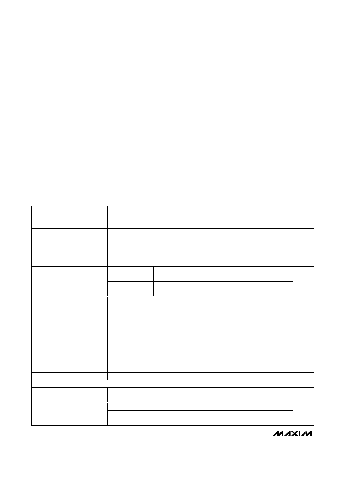
ABSOLUTE MAXIMUM RATINGS
ELECTRICAL CHARACTERISTICS
(V
IN1
= V
IN2
= V
IN3
= VDD= 3.6V, V
AGND
= V
PGND1
= V
PGND2
= 0V, circuit of Figure 2, TA= -40°C to +85°C, unless otherwise noted.
Typical values are at T
A
= +25°C.) (Note 1)
Stresses beyond those listed under “Absolute Maximum Ratings” may cause permanent damage to the device. These are stress ratings only, and functional
operation of the device at these or any other conditions beyond those indicated in the operational sections of the specifications is not implied. Exposure to
absolute maximum rating conditions for extended periods may affect device reliability.
IN1, IN2, IN3, VDDto AGND..................................-0.3V to +6.0V
SCL, SDA to AGND ....................................-0.3V to (V
DD
+ 0.3V)
IN1, IN2, IN3 to NEG .............................................-0.3V to +6.0V
AGND to C2N ........................................................-0.3V to +6.0V
C1P, C2P to AGND ....................................-0.3V to (V
IN1
+ 0.3V)
LED_, C1N, C2N to NEG............................-0.3V to (V
IN1
+ 0.3V)
LDO1, LDO2, REF to AGND ......................-0.3V to (V
IN3
+ 0.3V)
CMREF, AIN+, AIN-, SPK+, SPK-
to AGND..................................................-0.3V to (V
IN2
+ 0.3V)
IN1, IN2 to IN3.......................................................-0.3V to +0.3V
PGND1, PGND2 to AGND.....................................-0.3V to +0.3V
SPK+, SPK- Short Circuit to PGND2 or IN2 ...............Continuous
Continuous Power Dissipation (T
A
= +70°C)
28-Pin, Thin QFN 4mm x 4mm
(derate 28.6mW/°C above +70°C)..............................2286mW
Junction Temperature......................................................+150°C
Storage Temperature Range .............................-65°C to +150°C
Lead Temperature (soldering, 10s) .................................+300°C
PARAMETER CONDITIONS MIN TYP MAX UNITS
V
IN1
, V
IN2
, V
IN3
Operating
Voltage
2.7 5.5 V
VDD Operating Range 1.5 5.5 V
Undervoltage Lockout (UVLO)
Threshold
V
IN3
rising 2.25 2.45 2.65 V
UVLO Hysteresis 100 mV
VDD Shutdown Threshold 0.450 0.865 1.350 V
TA = +25°C 0.1 1
VDD = AGND
T
A
= +85°C 0.1
TA = +25°C 2 10
IN1, IN2, IN3 Shutdown Supply
Current
(All Outputs Off)
V
DD
= 3.6V
T
A
= +85°C 2
µA
Charge pump inactive, 2 LEDs at 0.1mA setting, audio
amplifier disabled, LDO1 and LDO2 disabled
70 120
LED driver disabled, audio amplifier disabled, and LDO1
and LDO2 enabled
170 250
µA
Charge pump active, 1MHz switching, all LEDs at
25.6mA setting, audio amplifier disabled, LDO1 and
LDO2 disabled
1.50 4.00
No-Load Supply Current
LED driver disabled, audio amplifier enabled, LDO1 and
LDO2 disabled
6.6 20
mA
Thermal Shutdown +160 °C
Thermal-Shutdown Hysteresis 20 °C
CHARGE PUMP
SYNC = 0 1000
SYNC = 1, SW_MODE = 00 450 550 650
SYNC = 1, SW_MODE = 01 575 700 825
Switching Frequency
(f
SW
)
SYNC = 1, SW_MODE = 10
625
± 25
kHz
Page 3
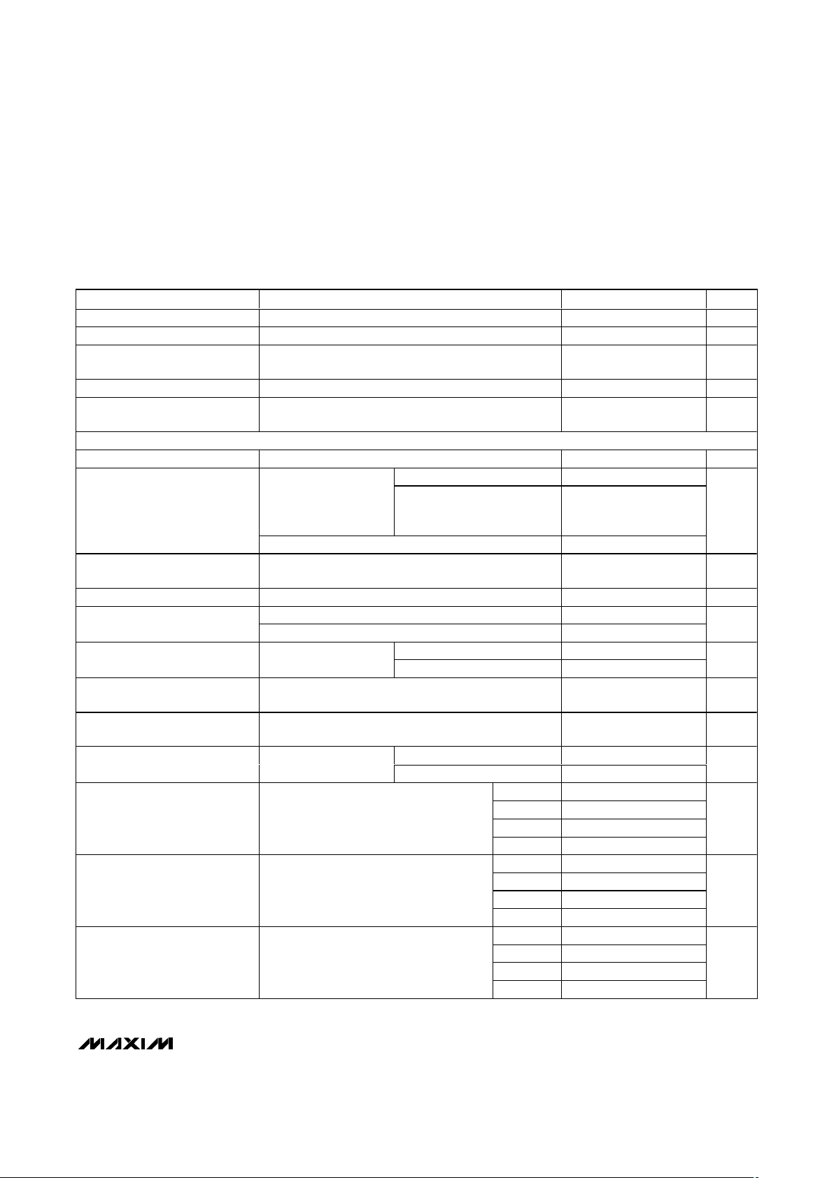
MAX8821
White LED Charge Pump with Mono Class D
Audio Amp and Dual LDO
_______________________________________________________________________________________ 3
PARAMETER CONDITIONS MIN TYP MAX UNITS
Soft-Start Time 0.1 ms
Regulation Voltage (V
IN1
- V
NEG
)5V
Open-Loop NEG Output
Resistance
(0.5 x V
IN1
- V
NEG
) / I
NEG
1.75 3.5 Ω
Output Current V
IN1
= 3.2V, LED V
FMAX
= 3.9V 154 mA
NEG Discharge Resistance in
Shutdown
All LEDs disabled 10 kΩ
LED_ CURRENT REGULATORS
Current Setting Range I
LED
_ 0.1 25.6 mA
TA = +25°C -2 ±1 +2
25.6mA setting
T
A
= -40°C to derating
function start temperature
(enabled by I
2
C)
-5 +5
Current Accuracy
0.1mA setting, T
A
= +25°C -30 ±5 +30
%
Current-Derating-Function Start
Temperature
+40 °C
Current-Derating-Function Slope TA = +40°C to +85°C -1.67 %/°C
Charge pump inactive 2.3 4.6
R
DS ON
Charge pump active 5 14
Ω
Charge pump inactive 72 120
Dropout Voltage 25.6mA setting (Note 2)
Charge pump active 120 360
mV
Current Regulator
Switchover Threshold
Charge pump inactive to active,
V
LED_
falling
125 150 175 mV
Current Regulator
Switchover Hysteresis
100 mV
TA = +25°C 0.01 1
Leakage Current in Shutdown
All LEDs
disabled
T
A
= +85°C 0.1
µA
00 524
01 1048
10 2097
Off Blink Time
B7, B6 or B3, B2,
SYNC = 0,
Table 11
11 4194
ms
00 66
01 131
10 262
On Blink Time
B5, B4 or B1, B0,
SYNC = 0,
Table 11
11 524
ms
00 262
01 524
10 1048
Ramp-Up/Down Time
LED__RU: B7, B6 or B3, B2
LED__RD: B5, B4 or B1, B0
SYNC = 0,
Tables 8, 9, 10 (Note 3)
11 2097
ms
ELECTRICAL CHARACTERISTICS (continued)
(V
IN1
= V
IN2
= V
IN3
= VDD= 3.6V, V
AGND
= V
PGND1
= V
PGND2
= 0V, circuit of Figure 2, TA= -40°C to +85°C, unless otherwise noted.
Typical values are at T
A
= +25°C.) (Note 1)
Page 4
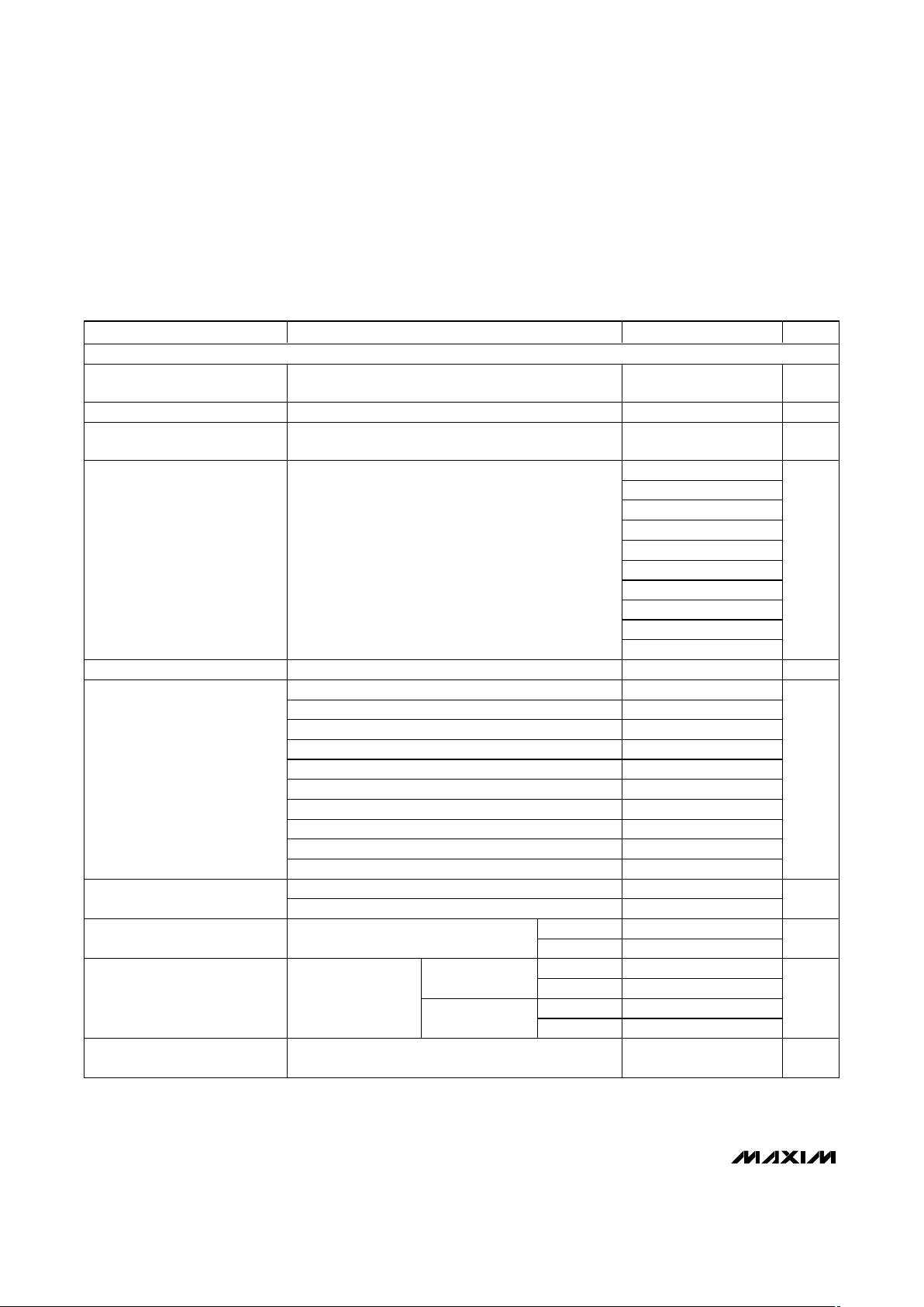
MAX8821
White LED Charge Pump with Mono Class D
Audio Amp and Dual LDO
4 _______________________________________________________________________________________
PARAMETER CONDITIONS MIN TYP MAX UNITS
AUDIO AMPLIFIER
Common-Mode Bias Voltage
0.95 x
(V
IN3
/ 2)
V
IN3
/ 2
1.05 x
(V
IN3
/ 2)
V
Output Offset Voltage V
AIN+
= V
AIN-
= V
IN3
/ 2, audio gain = 0dB ±1 mV
Common-Mode Input Voltage 0.5
V
IN3
-
1.2V
V
-3
0
3
6
9
12
15
18
21
Audio Gain Table 15, B3:B0
24
dB
Audio Gain Accuracy -3 +3 %
Audio gain = -3dB 54.4 99.0 143.5
Audio gain = 0dB 49.1 89.2 129.3
Audio gain = 3dB 43.1 78.4 113.7
Audio gain = 6dB 36.8 66.9 97.0
Audio gain = 9dB 30.5 55.5 80.5
Audio gain = 12dB 24.6 44.7 64.8
Audio gain = 15dB 19.3 35.2 51.0
Audio gain = 18dB 14.8 26.9 39.0
Audio gain = 21dB 11.1 20.2 29.3
Input Resistance
Audio gain = 24dB 8.2 15.0 22.0
kΩ
V
IN2
= V
IN3
= 3.6V 46
Common-Mode Rejection Ratio
f = 1kHz, V
IN2
= V
IN3
= 3.6V 46
dB
f = 217Hz 65
Power-Supply Rejection Ratio
V
AIN+
= V
AIN-
= V
IN3
/ 2,
100mV
P-P
at V
IN3 f = 20kHz 50
dB
RL = 8Ω 0.36 0.5
V
IN3
= 3.6V
R
L
= 4Ω 0.85
RL = 8Ω 0.8 1.1
Output Power
THD+N = 1%,
f = 1kHz
(Note 4)
V
IN3
= 5V
R
L
= 4Ω 2.0
W
Total Harmonic Distortion Plus
Noise
RL = 8Ω, f = 1kHz, P
OUT
= 0.25W,
V
IN2
= V
IN3
= 3.6V
0.05 %
ELECTRICAL CHARACTERISTICS (continued)
(V
IN1
= V
IN2
= V
IN3
= VDD= 3.6V, V
AGND
= V
PGND1
= V
PGND2
= 0V, circuit of Figure 2, TA= -40°C to +85°C, unless otherwise noted.
Typical values are at T
A
= +25°C.) (Note 1)
Page 5
MAX8821
PARAMETER CONDITIONS MIN TYP MAX UNITS
Fixed-frequency mode (FFM) 91
Spread-spectrum mode (SSM) 89
FFM A weighted 93
Signal-to-Noise Ratio
R
L
= 8Ω, f = 1kHz,
P
OUT
= 0.25W,
V
IN2
= V
IN3
= 3.6V
SSM A weighted 91
dB
SW_MODE = 00 900 1100 1300
SW_MODE = 01 1150 1400 1650
Oscillator Frequency
(f
osc
)
SW_MODE = 10
1250
±50
kHz
Differential Input
Resistance
Shutdown mode only 100 kΩ
Output Current Limit SPK+, SPK- short circuited to PGND2 or to IN2 2 A
Wake-Up Delay After
Short Circuit
110 µs
LDO1
Output Voltage V
LDO1
3.6V ≤ V
IN3
≤ 5.5V,
1mA ≤ I
LDO1
≤ 300mA
1.164 1.200
1.236 V
Maximum Output
Current
300 mA
Output Current Limit V
LDO1
= 0V 400 650 1000 mA
Dropout Voltage I
LDO1
= 200mA, T
A
= +25°C (Note 5) 150 300 mV
Line Regulation
V
IN3
stepped from 3.4V to 5.5V,
I
LDO1
= 150mA
2.4 mV
Load Regulation I
LDO1
stepped from 1mA to 300mA 25 mV
Power-Supply
Rejection
ΔV
IN3
/ΔV
LDO1
10Hz to 10kHz,
I
LDO1
= 30mA
70 dB
Output Voltage Noise
(RMS)
100Hz to 100kHz,
I
LDO1
= 30mA
45 µV
RMS
ELECTRICAL CHARACTERISTICS (continued)
(V
IN1
= V
IN2
= V
IN3
= VDD= 3.6V, V
AGND
= V
PGND1
= V
PGND2
= 0V, circuit of Figure 2, TA= -40°C to +85°C, unless otherwise noted.
Typical values are at T
A
= +25°C.) (Note 1)
White LED Charge Pump with Mono Class D
Audio Amp and Dual LDO
_______________________________________________________________________________________ 5
Page 6
MAX8821
White LED Charge Pump with Mono Class D
Audio Amp and Dual LDO
6 _______________________________________________________________________________________
PARAMETER CONDITIONS MIN TYP MAX UNITS
0000 1.164 1.2 1.236
0001 1.261 1.3 1.339
0010 1.455 1.5 1.545
0011 1.552 1.6 1.648
0100 1.746 1.8 1.854
0101 1.843 1.9 1.957
0110 1.940 2.0 2.060
0111 2.231 2.3 2.369
1000 2.425 2.5 2.575
1001 2.522 2.6 2.678
1010 2.619 2.7 2.781
1011 2.716 2.8 2.884
1100 2.813 2.9 2.987
1101 2.910 3.0 3.090
1110 3.007 3.1 3.193
Programmable Output
Voltage
I
LDO1
= 50mA
control bits B3:B0;
see Table 13
1111 3.104 3.2 3.296
V
Shutdown Output
Impedance
LDO1 disabled through I
2
C1kΩ
LDO2
Output Voltage V
LDO2
3.6V ≤ V
IN3
≤ 5.5V,
1mA ≤ I
LDO2
≤ 200mA
1.455 1.500
1.545 V
Maximum Output
Current
200 mA
Output Current Limit V
LDO2
= 0V 250 550 750 mA
Dropout Voltage I
LDO2
= 133mA, T
A
= +25°C (Note 5) 100 200 mV
Line Regulation V
IN3
stepped from 3.4V to 5.5V, I
LDO2
= 100mA 2.4 mV
Load Regulation I
LDO2
stepped from 1mA to 200mA 25 mV
Power-Supply
Rejection
ΔV
IN3
/ΔV
LDO2
10Hz to10kHz,
I
LDO2
= 20mA
70 dB
Output Voltage Noise
(RMS)
100Hz to100kHz,
I
LDO2
= 20mA
45 µV
RMS
ELECTRICAL CHARACTERISTICS (continued)
(V
IN1
= V
IN2
= V
IN3
= VDD= 3.6V, V
AGND
= V
PGND1
= V
PGND2
= 0V, circuit of Figure 2, TA= -40°C to +85°C, unless otherwise noted.
Typical values are at T
A
= +25°C.) (Note 1)
Page 7
MAX8821
White LED Charge Pump with Mono Class D
Audio Amp and Dual LDO
_______________________________________________________________________________________ 7
PARAMETER CONDITIONS MIN TYP MAX UNITS
0000 1.455 1.5 1.545
0001 1.552 1.6 1.648
0010 1.746 1.8 1.854
0011 1.940 2.0 2.060
0100 2.134 2.2 2.266
0101 2.231 2.3 2.369
0110 2.328 2.4 2.472
0111 2.425 2.5 2.575
1000 2.522 2.6 2.678
1001 2.619 2.7 2.781
1010 2.716 2.8 2.884
1011 2.813 2.9 2.987
1100 2.910 3.0 3.090
1101 3.007 3.1 3.193
1110 3.104 3.2 3.296
Programmable Output
Voltage
I
LDO2
= 50mA
control bits
B3:B0;
see Table 14
1111 3.201 3.3 3.399
V
Shutdown Output
Impedance
LDO2 disabled through I
2
C1kΩ
I2C INTERFACE (Figure 8)
Logic Input High
Voltage
0.7 x
V
DD
V
Logic Input Low
Voltage
0.3 x
V
DD
V
TA = +25°C -1 0.01 +1
Logic Input Current VIL = 0V or VIH = V
DD
TA = +85°C 0.1
µA
SDA Output Low
Voltage
I
SDA
= 3mA 0.03 0.4 V
I2C Clock Frequency 400 kHz
Bus-Free Time
Between START and
STOP
t
BUF
1.3 µs
Hold Time Repeated
START Condition
t
HD_STA
0.6 0.1 µs
SCL Low Period t
LOW
1.3 0.2 µs
SCL High Period t
HIGH
0.6 0.2 µs
Setup Time Repeated
START Condition
t
SU_STA
0.6 0.1 µs
ELECTRICAL CHARACTERISTICS (continued)
(V
IN1
= V
IN2
= V
IN3
= VDD= 3.6V, V
AGND
= V
PGND1
= V
PGND2
= 0V, circuit of Figure 2, TA= -40°C to +85°C, unless otherwise noted.
Typical values are at T
A
= +25°C.) (Note 1)
Page 8
MAX8821
White LED Charge Pump with Mono Class D
Audio Amp and Dual LDO
8 _______________________________________________________________________________________
Typical Operating Characteristics
(V
IN1
= V
IN2
= V
IN3
= VDD= 3.6V, V
AGND
= V
PGND1
= V
PGND2
= 0V, circuit of Figure 2, TA= +25°C, unless otherwise noted.)
PARAMETER CONDITIONS MIN TYP MAX UNITS
SDA Hold Time t
HD_DAT
0 -0.01 µs
SDA Setup Time t
SU_DAT
100 50 ns
Setup Time for STOP
Condition
t
SU_STO
0.6 0.1 µs
ELECTRICAL CHARACTERISTICS (continued)
(V
IN1
= V
IN2
= V
IN3
= VDD= 3.6V, V
AGND
= V
PGND1
= V
PGND2
= 0V, circuit of Figure 2, TA= -40°C to +85°C, unless otherwise noted.
Typical values are at T
A
= +25°C.) (Note 1)
Note 1: Limits are 100% production tested at T
A
= +25°C. Limits over the operating temperature range are guaranteed by design.
Note 2: Dropout voltage is defined as the LED_ to GND voltage when the current into LED_ drops 10% from the value at V
LED_
= 0.5V.
Note 3: Ramp-up time is from 0mA to full scale; ramp-down time is from full scale to 0mA.
Note 4: Output power is specified by a combination of a functional output current test and characterization analysis.
Note 5: The dropout voltage is defined as V
IN_
- V
OUT
when V
OUT
is 100mV below the nominal value of V
OUT
. The specification only
applies when V
OUT
≥ 3.0V.
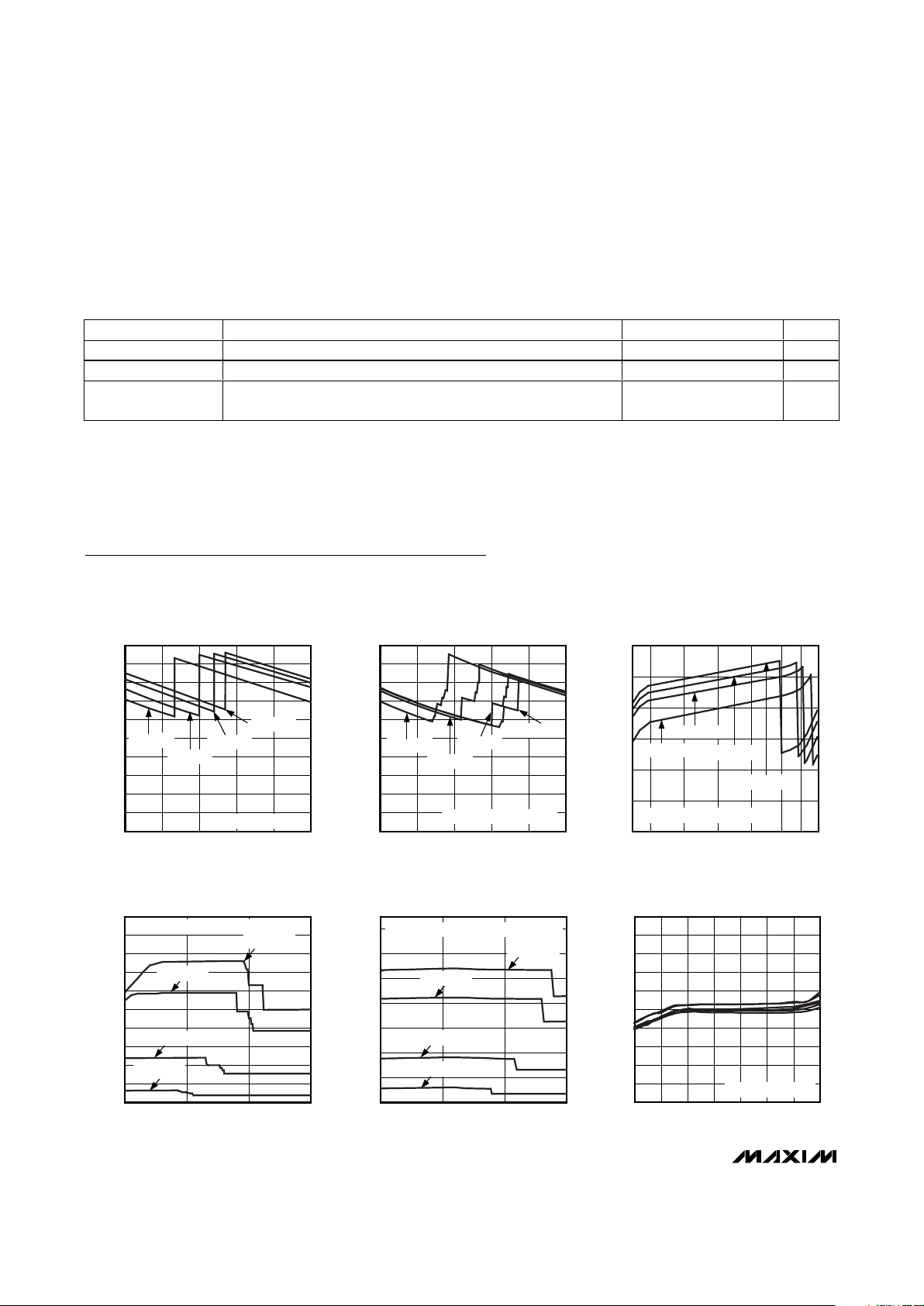
LED CHARGE PUMP
0
30
20
10
40
50
60
70
80
90
100
2.7 3.33.0 3.6 3.9 4.2
EFFICIENCY vs. SUPPLY VOLTAGE
(DRIVING SIX LEDS)
MAX8821 toc01
SUPPLY VOLTAGE (V)
EFFICIENCY (%)
1.6mA/LED
6.4mA/LED
20.8mA/LED
16mA/LED
LEDs HAVE MATCHED V
F
0
30
20
10
40
50
60
70
80
90
100
2.7 3.33.0 3.6 3.9 4.2
EFFICIENCY vs. SUPPLY VOLTAGE
(DRIVING SIX LEDS)
MAX8821 toc02
SUPPLY VOLTAGE (V)
EFFICIENCY (%)
1.6mA/LED
6.4mA/LED
20.8mA/LED
16mA/LED
LEDs HAVE MISMATCHED V
F
20.8mA/LED
40
60
50
80
70
90
100
4.2 3.7 3.63.9 3.8 3.5 3.4 3.0
EFFICIENCY vs. Li+ BATTERY VOLTAGE
DRIVING SIX LEDs
MAX8821 toc03
Li+ BATTERY VOLTAGE (V, TIME-WEIGHTED)
EFFICIENCY P
LED
/P
BATT
(%)
20.8mA/LED
16mA/LED
6.4mA/LED
1.6mA/LED
20.8mA/LEDLEDs HAVE HIGH MATCHED V
F
0
75
50
25
100
125
150
175
200
225
250
2.7 3.2
3.7
4.2
SUPPLY CURRENT
vs. SUPPLY VOLTAGE (DRIVING SIX LEDs)
MAX8821 toc04
SUPPLY VOLTAGE (V)
SUPPLY CURRENT (mA)
I
LED
= 20.8mA
I
LED
= 16mA
I
LED
= 6.4mA
I
LED
= 1.6mA
LEDs HAVE HIGH MISMATCHED V
F
SUPPLY CURRENT
vs. SUPPLY VOLTAGE (RGB MODULE)
MAX8821 toc05
SUPPLY VOLTAGE (V)
SUPPLY CURRENT (mA)
3.73.2
10
20
30
40
50
60
70
0
2.7 4.2
I
LED
= 20.8mA
I
LED
= 16mA
I
LED
= 6.4mA
I
LED
= 1.6mA
RGB MODULE: LUMEX SML-LX3632SISUGSBC
LED CURRENT MATCHING
vs. SUPPLY VOLTAGE (16mA/LED)
MAX8821 toc06
SUPPLY VOLTAGE (V)
LED CURRENT (mA)
5.14.73.9 4.33.53.1
15.6
15.7
15.8
15.9
16.0
16.1
16.2
16.3
16.4
16.5
15.5
2.7 5.5
CHARGE PUMP IN 1.5x
Page 9
MAX8821
White LED Charge Pump with Mono Class D
Audio Amp and Dual LDO
_______________________________________________________________________________________
9
Typical Operating Characteristics (continued)
(V
IN1
= V
IN2
= V
IN3
= VDD= 3.6V, V
AGND
= V
PGND1
= V
PGND2
= 0V, circuit of Figure 2, TA= +25°C, unless otherwise noted.)
LED CURRENT vs. AMBIENT
TEMPERATURE
MAX8821 toc07
TEMPERATURE (°C)
LED CURRENT (mA)
806040200-20
5
10
15
20
25
30
0
-40 100
CURRENT DERATING ENABLED
400ns/div
1x MODE OPERATING
WAVEFORMS (V
IN
= 4V)
V
IN
V
NEG
200mA/div
AC-COUPLED
100mV/div
MAX8821 toc08
I
IN
I
LED
ALL LEDs ON, I
LED
= 25.6mA
2V/div
0V
0A
20mA/div
0A
400ns/div
1.5x MODE OPERATING
WAVEFORMS (V
IN
= 3V)
V
IN
V
NEG
200mA/div
AC-COUPLED
100mV/div
MAX8821 toc09
I
IN
I
LED
ALL LEDs ON, I
LED
= 25.6mA
2V/div
0A
20mA/div
0A
0V
1ms/div
LED LINE TRANSIENT WITH MODE CHANGE
(V
IN
= 3.8V TO 3.4V TO 3.8V)
V
IN
200mA/div
3.8V
MAX8821 toc10
I
IN
I
LED6
ALL LEDs AT 25.6mA SETTING
0A
20mA/div
0A
3.4V
1ms/div
LED LINE TRANSIENT WITH MODE CHANGE
(V
IN
= 4.2V TO 3.8V TO 4.2V)
V
IN
200mA/div
4.2V
MAX8821 toc11
I
IN
I
LED6
ALL LEDs AT 25.6mA SETTING
0A
20mA/div
0A
3.8V
1ms/div
LED STARTUP WAVEFORMS
(V
IN
= 4V)
V
IN
50mA/div
AC-COUPLED
50mV/div
MAX8821 toc12
I
IN
I
LED6
0A
20mA/div
0A
1ms/div
LED SHUTDOWN WAVEFORMS
(V
IN
= 4V)
V
IN
50mA/div
AC-COUPLED
MAX8821 toc13
I
IN
I
LED6
0A
20mA/div
0A
50mV/div
400ms/div
LED RAMP-UP
10mA/div
MAX8821 toc14
I
LED6
I
LED5
0A
0A
10mA/div
Page 10

MAX8821
White LED Charge Pump with Mono Class D
Audio Amp and Dual LDO
10 ______________________________________________________________________________________
Typical Operating Characteristics (continued)
(V
IN1
= V
IN2
= V
IN3
= VDD= 3.6V, V
AGND
= V
PGND1
= V
PGND2
= 0V, circuit of Figure 2, TA= +25°C, unless otherwise noted.)
-140
-120
-100
-80
-60
-40
-20
0
20
0 5 10 15 20
FIXED-FREQUENCY-MODE OUTPUT
SPECTRUM vs. FREQUENCY
MAX8821 toc19
FREQUENCY (kHz)
AMPLITUDE (dBV)
RL = 8Ω
V
BATT
= 5V
V
OUT
= -60dBV
UNWEIGHTED
FFM -1100kHz
-140
-120
-100
-80
-60
-40
-20
0
20
0 5 10 15 20
SPREAD-SPECTRUM-MODE OUTPUT
SPECTRUM vs. FREQUENCY
MAX8821 toc18
FREQUENCY (kHz)
AMPLITUDE (dBV)
RL = 8Ω
V
BATT
= 5V
V
OUT
= -60dBV
UNWEIGHTED
AUDIO AMPLIFIER PHASE
vs. FREQUENCY
MAX8821 toc21
FREQUENCY (kHz)
PHASE (°)
101
-50
-40
-30
-20
-10
0
10
20
-60
0.1 100
TOTAL HARMONIC DISTORTION
PLUS NOISE vs. FREQUENCY
MAX8821 toc15
FREQUENCY (kHz)
THD+N (%)
1010.1
0.1
0.01 100
1
0.01
P
OUT
= 25mW
P
OUT
= 350mW
P
OUT
= 100mW
VIN = 3.6V
R
L
= 8
Ω
TOTAL HARMONIC DISTORTION
vs. OUTPUT POWER
MAX8821 toc16
OUTPUT POWER (W)
THD+N (%)
0.80.60.40.2
0.1
1
10
100
0.01
0 1.0
VIN = 3.6V
R
L
= 8
Ω
TOTAL HARMONIC DISTORTION
vs. OUTPUT POWER
MAX8821 toc17
OUTPUT POWER (W)
THD+N (%)
2.52.01.51.00.5
0.1
1
10
100
0.01
03.0
VIN = 5V
R
L
= 4
Ω
11.75
11.90
11.85
11.80
11.95
12.00
12.05
12.10
12.15
12.20
12.25
0 5 10 15 20
AUDIO AMPLIFIER GAIN
vs. FREQUENCY
MAX8821 toc20
FREQUENCY (kHz)
GAIN (dB)
AUDIO AMPLIFIER PSRR
vs. FREQUENCY
MAX8821 toc22
FREQUENCY (kHz)
PSRR (dB)
1
-90
-80
-70
-60
-50
-40
-30
-20
-10
0
-100
0.1 10
V
RIPPLE
= 100mV
P-P
AUDIO GAIN = 0dB
R
L
= 4
Ω
C
CMREF
= 0.1μF
C
CMREF
= 1μF
WIDEBAND OUTPUT SPECTRUM
SPREAD-SPECTRUM MODE
MAX8821 toc23
FREQUENCY (MHz)
AMPLITUDE (dBV)
1010.10.01
-120
-100
-80
-60
-40
-20
0
-140
0.001 100
RL = 8
Ω
INPUTS AC GROUNDED
CLASS D AMP
Page 11

MAX8821
White LED Charge Pump with Mono Class D
Audio Amp and Dual LDO
______________________________________________________________________________________
11
WIDEBAND OUTPUT SPECTRUM
FIXED-FREQUENCY MODE
MAX8821 toc24
FREQUENCY (MHz)
AMPLITUDE (dBV)
1010.10.01
-120
-100
-80
-60
-40
-20
0
-140
0.001 100
RL = 8
Ω
INPUTS AC GROUNDED
0
0.5
1.5
1.0
2.0
2.5
2.7 3.53.1 3.9 4.3 4.7 5.1 5.5
OUTPUT POWER
vs. SUPPLY VOLTAGE
MAX8821 toc25
SUPPLY VOLTAGE (V)
OUTPUT POWER (W)
THD+N = 10%
THD+N = 1%
RL = 8Ω
0
1.0
0.5
2.0
1.5
3.0
2.5
3.5
2.7 3.5 3.93.1 4.3 4.7 5.1 5.5
OUTPUT POWER
vs. SUPPLY VOLTAGE
MAX8821 toc26
SUPPLY VOLTAGE (V)
OUTPUT POWER (W)
THD+N = 10%
THD+N = 1%
RL = 4Ω
50
65
60
55
75
70
95
90
85
80
100
2.7 3.1 3.5 3.9 4.3 4.7 5.1 5.5
EFFICIENCY
vs. SUPPLY VOLTAGE
MAX8821 toc27
SUPPLY VOLTAGE (V)
EFFICIENCY (%)
RL = 8Ω
RL = 4Ω
0
30
20
10
40
50
60
70
80
90
100
0 0.5 1.0 1.5 2.0
EFFICIENCY vs. OUTPUT POWER
MAX8821 toc28
OUTPUT POWER (W)
EFFICIENCY (%)
RL = 8Ω
RL = 4Ω
VIN = 3.6V
0
30
20
10
40
50
60
70
80
90
100
01234
EFFICIENCY
vs. OUTPUT POWER
MAX8821 toc29
OUTPUT POWER (W)
EFFICIENCY (%)
RL = 8Ω
RL = 4Ω
VIN = 5V
Typical Operating Characteristics (continued)
(V
IN1
= V
IN2
= V
IN3
= VDD= 3.6V, V
AGND
= V
PGND1
= V
PGND2
= 0V, circuit of Figure 2, TA= +25°C, unless otherwise noted.)
Page 12

MAX8821
White LED Charge Pump with Mono Class D
Audio Amp and Dual LDO
12 ______________________________________________________________________________________
Typical Operating Characteristics
(V
IN1
= V
IN2
= V
IN3
= VDD= 3.6V, V
AGND
= V
PGND1
= V
PGND2
= 0V, circuit of Figure 2, TA= +25°C, unless otherwise noted.)
STARTUP WAVEFORMS
MAX8821 toc30
1V/div
1V/div
AIN+ - AIN-
SPK+ - SPK-
0V
0V
AV = 0dB
SHUTDOWN WAVEFORMS
MAX8821 toc31
1V/div
1V/div
AIN+ - AIN-
SPK+ - SPK-
0V
0V
AV = 0dB
0
60
40
20
80
100
120
140
160
180
200
010050 150 200 250 300
LDO DROPOUT VOLTAGE
vs. LOAD CURRENT
MAX8821 toc32
LOAD CURRENT (mA)
DROPOUT VOLTAGE (mV)
LDO1
LDO2
LDO OUTPUT VOLTAGE
ACCURACY vs. LOAD CURRENT
MAX8821 toc33
LOAD CURRENT (mA)
OUTPUT VOLTAGE ACCURACY (%)
25020015010050
-4
-3
-2
-1
0
1
-5
0300
V
LDO2
= 2.8V
V
LDO1
= 2.8V
LDO OUTPUT VOLTAGE
vs. TEMPERATURE
MAX8821 toc34
TEMPERATURE (°C)
OUTPUT VOLTAGE (V)
603510-15
2.65
2.70
2.75
2.80
2.85
2.90
2.60
-40 85
I
LDO1
= 0A
I
LDO2
= 0A
I
LDO2
= 100mA
I
LDO1
= 100mA
DUAL LDOs
LDO PSRR
vs. FREQUENCY
MAX8821 toc35
FREQUENCY (kHz)
PSRR (dB)
1010.1
-80
-70
-60
-50
-40
-30
-20
-10
0
-90
0.01 100
I
LDO2
= 20mA
I
LDO1
= 30mA
V
IN-RIPPLE
= 100mV
P-P
Page 13

MAX8821
White LED Charge Pump with Mono Class D
Audio Amp and Dual LDO
______________________________________________________________________________________
13
10μs/div
LDO2 LOAD TRANSIENT
MAX8821 toc39
AC-COUPLED
50mV/div
V
LDO2
I
LDO2
0A
50mA/div
2ms/div
LDO SHUTDOWN RESPONSE
(LDO1, LDO2 UNLOADED)
MAX8821 toc40
V
LDO1
V
LDO2
0V
0V
1V/div
1V/div
Typical Operating Characteristics
(V
IN1
= V
IN2
= V
IN3
= VDD= 3.6V, V
AGND
= V
PGND1
= V
PGND2
= 0V, circuit of Figure 2, TA= +25°C, unless otherwise noted.)
200μs/div
LDO LINE TRANSIENT
(V
IN3
= 3.6V TO 4.5V)
MAX8821 toc37
4.5V
3.6V
AC-COUPLED
10mV/div
AC-COUPLED
10mV/div
V
IN
V
LDO1
V
LDO2
I
LDO1
= 150mA, I
LDO2
= 100mA
10μs/div
LDO1 LOAD TRANSIENT
MAX8821 toc38
AC-COUPLED
50mV/div
V
LDO1
I
LDO1
0A
50mA/div
LDO OUTPUT SPECTRUM
MAX8821 toc36
FREQUENCY (kHz)
AMPLITUDE (dBV)
100100.01 0.1 1
-140
-120
-100
-80
-60
-40
-20
0
-160
0.001 1000
Page 14

MAX8821
White LED Charge Pump with Mono Class D
Audio Amp and Dual LDO
14 ______________________________________________________________________________________
Pin Description
PIN NAME FUNCTION
1V
DD
I2C Input Supply Voltage. The VDD supply range is 1.5V to 5.5V. Drive VDD high to enable the I2C
control. Drive V
DD
low to place the IC into shutdown mode.
2 CMREF
Audio Common-Mode Reference Voltage. Bypass CMREF with a 0.1µF ceramic capacitor to AGND
as close as possible to the IC.
3 AIN+ Noninverting Audio Input
4 AIN- Inverting Audio Input
5 PGND2 Audio Amplifier Power Ground. Connect PGND2 to the system ground plane.
6 SPK- Audio Amplifier Negative Output
7 SPK+ Audio Amplifier Positive Output
8 IN2
Audio Amplifier Output Buffer Supply Voltage Input. The input voltage range is 2.7V to 5.5V. Connect
IN2 directly to IN1 and IN3. Bypass IN2 to PGND2 with a 1µF ceramic capacitor as close as possible
to the IC. IN2 is high impedance during shutdown.
9 LDO2
200mA LDO Output. Bypass LDO2 to AGND with a 1µF ceramic capacitor. LDO2 is disabled through
the I
2
C interface.
10 LDO1
300mA LDO Output. Bypass LDO1 to AGND with a 2.2µF ceramic capacitor. LDO1 is disabled
through the I
2
C interface.
11 SCL I2C Clock Input. Data is read on the rising edge of V
SCL
.
12 SDA I2C Data Input. Data is read on the rising edge of V
SCL.
.
13 AGND
Analog Ground. Connect AGND to the system ground plane. AGND is also internally connected to
the exposed paddle.
14 REF Refer ence Byp ass. Byp ass RE F w i th a 0.1µF cer am i c cap aci tor to AG N D as cl ose as p ossi b l e to the IC .
15–20
LED1–
LED6
LED Current Regulators. Current flowing into LED_ is based upon the internal I
2
C registers. Connect
LED_ to the cathodes of the external LEDs. LED_ is high impedance during shutdown. If unused,
short LED_ to IN1 to disable the regulator.
21 NEG
Charge-Pump Negative Output. Connect a 1µF ceramic capacitor from NEG to AGND. In shutdown,
an internal 10kΩ resistor connects NEG to AGND.
22 C2N Transfer Capacitor 2 Negative Connection. Connect a 1µF ceramic capacitor from C2P to C2N.
23 C1N Transfer Capacitor 1 Negative Connection. Connect a 1µF ceramic capacitor from C1P to C1N.
24 C2P Transfer Capacitor 2 Positive Connection. Connect a 1µF ceramic capacitor from C2P to C2N.
25 C1P Transfer Capacitor 1 Positive Connection. Connect a 1µF ceramic capacitor from C1P to C1N.
26 IN1
Charge-Pump Supply Voltage Input. The input voltage range is 2.7V to 5.5V. Connect IN1 directly to
IN2 and IN3. Bypass IN1 to PGND1 with a 2.2µF ceramic capacitor as close as possible to the IC.
IN1 is high impedance during shutdown.
27 PGND1 Charge-Pump Power Ground. Connect PGND1 to the system ground plane.
28 IN3
Input Voltage Supply for LDO1, LDO2, REF, Class D Preamplifier, and Class D Amplifier Modulator
Core. The input voltage range is 2.7V to 5.5V. Connect IN3 directly to IN1 and IN2. Bypass IN3 to
AGND with a 2.2µF ceramic capacitor as close as possible to the IC. IN3 is high impedance during
shutdown.
—EP
Exposed Paddle. Connect the exposed paddle to AGND directly under the IC. Exposed paddle is
internally connected to AGND.
Page 15

MAX8821
White LED Charge Pump with Mono Class D
Audio Amp and Dual LDO
______________________________________________________________________________________ 15
SDA
SCL
PGND1
REF
AGND
LED3
LED4
LED5
LED6
LED1
EP
INVERTING
CHARGE PUMP
CURRENT
SOURCE
CONTROL
IN1
REFERENCE
IN3
LED2
CMREF
SELECT
MINIMUM
I
2
C INTERFACE AND
LOGIC CONTROL
LDO1
LDO2
LDO1
LDO2
SPK+
SPK-
CLASS D
AMP
PGND2
IN2
PGA
AIN-
AIN+
ADAPTIVE
CURRENT
REGULATORS
OSCILLATOR
NEG
NEG
NEG
NEG
NEG
NEG
NEG
REF
PGND2
PGND2
OUTPUT
BUFFER
V
DD
IN3
C2NC2PC1NC1P
MAX8821
+
-
OSCILLATOR
Figure 1. Block Diagram
Page 16

MAX8821
White LED Charge Pump with Mono Class D
Audio Amp and Dual LDO
16 ______________________________________________________________________________________
Detailed Description
The MAX8821 integrates a charge pump for white LED
display backlighting, an audio loudspeaker amplifier,
and dual LDO for camera functions. It includes softstart, thermal shutdown, open-circuit and short-circuit
protections for the white LEDs, audio amplifier, and
LDOs. Figure 1 is the block diagram, and Figure 2
shows the typical application circuit.
LED Charge Pump
The MAX8821 features an inverting charge pump and
six current regulators capable of 25.6mA each to drive
six LEDs. The current regulators are matched to within
±1% (typ), providing uniform white LED brightness for
LCD backlight applications. To maximize efficiency, the
current regulators operate with as little as 0.15V voltage
drop. Individual white LED current regulators conduct
current to GND or NEG to extend usable battery life. In
the case of mismatched forward voltage of white LEDs,
only the white LEDs requiring higher voltage are
switched to direct current to NEG instead of GND, further raising efficiency and reducing battery current
drain. The regulation scheme is optimized to ensure
low EMI and low input ripple. The on-chip ambient temperature derating function safely allows bright 25.6mA
NEG
LED1
LED5
LED4
LED3
LED2
LED6
DUAL LOWNOISE LDO
LOUDSPEAKER/EARPIECE
SPK+
SPK-
INDIVIDUAL
0.1mA TO
25.6mA
DIMMING
PGND1
IN1
CMREF
IN3
REF
AGND
IN2
PGND2
AIN+
AIN-
V
DD
SDA
SCL
DIFFERENTIAL
AUDIO INPUT
LOGIC
CONTROL AND I
2
C
INTERFACE
EP
C7
2.2μF
C3
1μF
C5
2.2μF
C4
0.1μF
C12
0.1μF
C1P C1N
C8
1
μ
F
C2P C2N
C9
1
μ
F
C6
1
μ
F
LDO1
LDO2
C10
2.2
μ
F
C11
1
μ
F
INPUT
2.7 TO 5.5V
MAX8821
Figure 2. Typical Application Circuit
Page 17

MAX8821
White LED Charge Pump with Mono Class D
Audio Amp and Dual LDO
______________________________________________________________________________________ 17
full-scale output current while automatically reducing
current gradually above +40°C in accordance with
popular LED ratings. The on-chip derating feature can
be enabled, or disabled, using the I
2
C interface.
Current Regulator Switchover
When VINis higher than the forward voltage of the white
LED plus the 0.15V headroom of the current regulator,
the LED current returns through ground. If this condition is satisfied for all six white LEDs the charge pump
remains inactive. When the input voltage drops so that
the current regulator head room cannot be maintained
for any of the individual white LEDs, the inverting
charge pump activates and generates a voltage on
NEG that is no greater than 5V below VIN. Each current
regulator contains circuitry that detects when it is in
dropout and switches that current regulator return path
from GND to NEG. Since this is done on an LED-byLED basis, the LED current is switched for only the individual LED requiring higher voltage, thus minimizing
power consumption.
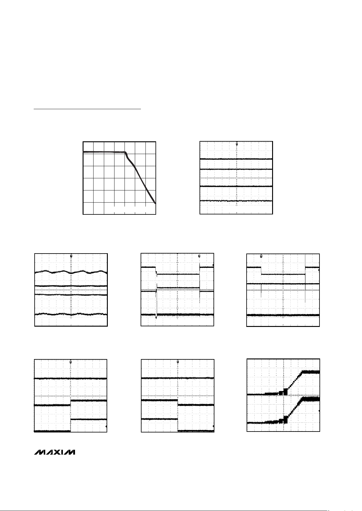
Ramp-Up and Ramp-Down Function
The LED drivers in the MAX8821 provide ramp-up and
ramp-down of LED current for smooth transitions
between different brightness settings. A controlled
ramp is used when the LED current level is changed,
when the LEDs are enabled, and when the LEDs are
disabled. The LED currents ramp up and down smoothly on a pseudo-log scaling of the LED current sources
(Figures 3 and 4). Each LED source has an individual
ramp control making it possible to ramp different LEDs
at different rates. The ramp-up and ramp-down (t
RAMP
)
LED current times are controlled by the LED_RU and
LED_RD control bits (Tables 8, 9, and 10). The
LED_RP_EN bit enables and disables the ramps. The
MAX8821 increases/decreases the current one step
every t
RAMP
/32 until the desired current is reached.
Blink Timer
The current regulators for LED5 and LED6 feature a
blink function. The OFF and ON time for LED5 and
LED6 can be set using the I2C interface (Table 11). See
Figure 5.
Combining Blink Timer and Ramp Function
To combine the ramp function together with the blink
timer for LED5 and/or LED6, special timing considerations need to be fulfilled. It is recommended to keep the
ramp-up timer shorter than the ON blink timer and the
ramp-down timer shorter than the OFF blink timer.
Failing to comply with these timing constraints results in
the LED_ not reaching the programmed current
(LED_[4:0], Tables 6 and 7) during the ON time and the
LED_ current not returning to 0mA during the off time.
See the following equations to ensure proper operation:
where LED_[4:0] is the programmed current set by I2C
(see Tables 6 and 7).
Figure 6 shows combining ramp function and blink timer.
LED Short- and Open-Circuit Protection
If any LED fails as an open circuit, the corresponding
LED_ is internally connected to ground and the charge
pump is enabled. To disable the corresponding current
regulator, short any unused LED_ to IN1. The MAX8821
contains special circuitry to detect this condition and
disables the corresponding current regulator to avoid
wasting battery power.
Temperature Derating
The MAX8821 contains a derating function that automatically limits the LED current at high temperatures in
accordance with the recommended derating curve of
popular white LEDs. The derating function enables the
safe usage of higher LED current at room temperature,
thus reducing the number of LEDs required to backlight
the display. The derating circuit limits the LED current
by reducing the LED current above +40°C at approximately 1.67%/°C. The temperature derating function is
enabled/disabled using the I2C interface and by default
is disabled.
t
t
LED
t
t
LED
ON BLINK
LED RU
OFF BLINK
LED RD
_
_
_
_
(_[:])
(_[:])
≥+
≥+
32
40 1
32
40 1
t
RAMP
=
2097ms
t
RAMP
=
1048ms
t
RAMP
=
524ms
t
RAMP
=
262ms
I
LED_
= 25.6mA
I
LED_
= 0
Figure 3. Ramp-Up Behavior
t
RAMP
=
2097ms
t
RAMP
=
1048ms
t
RAMP
=
524ms
t
RAMP
=
262ms
I
LED_
= 25.6mA
I
LED_
= 0
Figure 4. Ramp-Down Behavior
Page 18

MAX8821
White LED Charge Pump with Mono Class D
Audio Amp and Dual LDO
18 ______________________________________________________________________________________
Audio Amplifier
The audio amplifier in the MAX8821 is a 2W Class D
loudspeaker amplifier. The amplifier features a lowpower shutdown mode and industry-leading click-andpop suppression. The amplifier also features a
programmable gain control through an I
2
C interface.
The amplifier operates from a single 2.7V to 5.5V supply (V
IN3
= V
IN2
) and features an internally generated
common-mode bias voltage of V
IN3
/ 2 referenced to
ground.
Click-and-Pop Suppression
The MAX8821 features Maxim’s industry-leading clickand-pop suppression circuitry. During startup, the
amplifier’s common-mode bias voltage ramps to the
DC bias point. When entering shutdown, the amplifier
outputs are high impedance with 100kΩ between both
inputs. This scheme minimizes the energy present in
the audio band.
Class D Amplifier
The MAX8821 ultra-low-EMI, filterless, Class D audio
power amplifier features several improvements to
switch mode amplifier technology. The MAX8821 audio
amplifier features output driver AEL circuitry to reduce
EMI. Zero dead-time technology maintains state-of-theart efficiency and THD+N performance by allowing the
output MOSFETs to switch simultaneously without
cross-conduction.
A unique filterless modulation scheme and spreadspectrum mode create a compact, flexible, low-noise,
efficient audio power amplifier while occupying minimal
board space. The differential input architecture reduces
common-mode noise pickup with or without the use of
input-coupling capacitors. The MAX8821 audio amplifier
can also be configured as a single-ended input amplifier
without performance degradation. The input capacitors
C
IN
(Figure 7) are required for single-ended input appli-
cations and are typically 1µF.
The output of the MAX8821 shuts down if the output current reaches approximately 2A. Each output MOSFET
has its own short-circuit protection. This protection
scheme allows the amplifier to survive shorts to either
supply rail. After a thermal overload or short circuit, the
device remains disabled for a minimum of 110µs before
attempting to return to normal operation. The amplifier
shuts down immediately and waits another 110µs before
turning on if the fault condition remains. This operation
causes the output to pulse during a persistent fault.
Comparators monitor the MAX8821 inputs and compare
the complementary input voltages to the sawtooth waveform. The comparators trip when the input magnitude of
the sawtooth exceeds their corresponding input voltage.
Both comparators reset at a fixed time after the rising
edge of the second comparator trip point, generating a
minimum width pulse t
ON(MIN)
at the output of the second comparator. As the input voltage increases or
decreases, the duration of the pulse at one output
increases (the first comparator to trip), while the other
output pulse duration remains at t
ON(MIN)
. This causes
the net voltage across the speaker (SPK+ - SPK-)
to change.
Adjustable Differential Gain
The audio amplifier has an internal gain control. The
gain of the input amplifiers is controlled through the I2C
interface. The gain setting of the input amplifier can be
set from -3dB to +24dB (Table 15). This allows the
amplifier to be used for both hands-free and for receiver mode without any external components.
Input Filter
The fully differential amplifier inputs can be biased at
voltages other than midsupply. The common-mode
feedback circuit adjusts for input bias, ensuring the
outputs are still biased at midsupply. Input capacitors
are not required as long as the common-mode input
voltage is within the specified range listed in the
Electrical Characteristics
table. If input capacitors are
used, input capacitor CIN, in conjunction with on-chip
R
INT
, forms a highpass filter that removes the DC bias
from an incoming signal. The AC-coupling capacitor
allows the amplifier to bias the signal to an optimum DC
level. Assuming zero-source impedance, the -3dB point
of the highpass filter is given by:
Setting the -3dB corner too high affects the low-frequency response of the amplifier. Use capacitors with
dielectrics that have low-voltage coefficients, such as
aluminum electrolytic. Capacitors with high voltage
coefficients, such as ceramics, can increase distortion
at low frequencies.
f
RC
dB
INT IN
−
=
×× ×
3
1
2 π
64ms = t
ON_BLINK
= 512ms
0.512s = t
OFF_BLINK
= 4.098s
ILED6[4:0]
ILED5[4:0]
Figure 5. Blink Timer Behavior
Page 19

MAX8821
White LED Charge Pump with Mono Class D
Audio Amp and Dual LDO
______________________________________________________________________________________ 19
LDO1 and LDO2
The linear regulators are designed for low dropout and
low quiescent current to maximize battery life. Both
LDOs are controlled through the I2C interface, minimizing the number of control lines to the MAX8821. Each
LDO has an individual control register (LDO1_CNTL
and LDO2_CNTL, Tables 13 and 14). The I2C interface
controls the output voltages, and the enable/disable
state for both LDO1 and LDO2.
Thermal Shutdown
The MAX8821 includes a thermal-limit circuit that shuts
down the IC at a junction temperature of approximately
+160°C. The IC turns on after it cools by approximately
20°C.
Shutdown Mode
The MAX8821 can be put into two different shutdown
modes. The first shutdown mode is achieved by driving
VDDlow. In this mode, the I2C interface becomes disabled. The second shutdown is a lower power mode.
To enter the low-power mode, disable LED_, audio
amplifier, and LDOs through I2C. In lower power mode,
the I2C interface is still active.
I2C Interface
The I2C serial interface consists of a serial-data line
(SDA) and a serial-clock line (SCL). Standard I2C writebyte commands are used. Figure 8 shows a timing diagram for the I2C protocol. The MAX8821 is a slave-only
device, relying upon a master to generate a clock signal. The master (typically a microprocessor) initiates
data transfer on the bus and generates SCL to permit
data transfer. A master device communicates to the
MAX8821 by transmitting the proper 8-bit address followed by the 8-bit control byte. Each transmit
sequence is framed by a START (A) condition and a
STOP (L) condition. Each word transmitted over the bus
is 8 bits long and is always followed by an acknowledge clock pulse (K).
Both SCL and SDA remain high when the interface is
not busy. A master signals the beginning of a transmission with a START (A) condition by transitioning SDA
from high to low while SCL is high. When the master
has finished communicating with the slave, the master
issues a STOP (L) condition by transitioning SDA from
low to high while SCL is high. The bus is then free for
another transmission. One data bit is transferred during
each clock pulse. The data on SDA must remain stable
while SCL is high.
Register Reset
The I2C register is reset back to the default value when
either V
IN_
drops below the UVLO threshold or VDDis
driven low.
I2C Registers and Control
I
2
C Address
The MAX8821 acts as a slave transmitter/receiver. The
slave address of the MAX8821 is preset to 1001110X,
where “X” is the R/W bit. The address 0x9C is designated for write operations and 0x9D for read operations.
Use Table 1 as a register map to reference the control
bits found in Tables 2–16.
t
OFF_BLINK
t
ON_BLINK
t
OFF_BLINK
ILED_ = LED_ [4.0]
ILED_ = 0mA
t = t
LED_RU
/32 t = t
LED_RD
/32
Figure 6. Combining Ramp Function and Blink Timer (Tables 10 and 11)
MONO
CLASS D
AUDIO AMP
EARPIECE/
LOUDSPEAKER
CIN
CIN
R
INT
R
INT
MAX8821
AUDIO
INPUTS
Figure 7. Optional Input Capacitors
Page 20

MAX8821
White LED Charge Pump with Mono Class D
Audio Amp and Dual LDO
20 ______________________________________________________________________________________
SCL
A
B
C
D
E F
G
H
I
J
K
SDA
t
HD_STA
L
M
J = ACKNOWLEDGE CLOCKED INTO MASTER
K = ACKNOWLEDGE CLOCK PULSE
L = STOP CONDITION, DATA EXECUTED BY SLAVE
M = NEW START CONDITION
t
BUF
t
LOW
t
HIGH
t
SU_STA
t
SU_DAT
t
HD_DAT
t
SU_STO
F = ACKNOWLEDGE BIT CLOCKED INTO MASTER
G = MSB OF DATA CLOCKED INTO SLAVE (OP/SUS BIT)
H = LSB OF DATA CLOCKED INTO SLAVE
I = SLAVE PULLS SMBDATA LINE LOW
A = START CONDITION
B = MSB OF ADDRESS CLOCKED INTO SLAVE
C = LSB OF ADDRESS CLOCKED INTO SLAVE
D = R/W BIT CLOCKED INTO SLAVE
E = SLAVE PULLS SMBDATA LINE LOW
Figure 8. I2C Timing Diagram
NAME
GROUP ADDRESS
(hexadecimal)
TABLE TYPE DESCRIPTION
LED1_CNTL 00 2 R/W LED1 current regulator control
LED2_CNTL 01 3 R/W LED2 current regulator control
LED3_CNTL 02 4 R/W LED3 current regulator control
LED4_CNTL 03 5 R/W LED4 current regulator control
LED5_CNTL 04 6 R/W LED5 current regulator control
LED6_CNTL 05 7 R/W LED6 current regulator control
RAMP1_CNTL 06 8 R/W LED1 and LED2 ramp control
RAMP2_CNTL 07 9 R/W LED3 and LED4 ramp control
RAMP3_CNTL 08 10 R/W LED5 and LED6 ramp control
BLINK_CNTL 09 11 R/W LED5 and LED6 blink control
LED_EN 0A 12 R/W LED1–LED6 enable control
LDO1_CNTL 0B 13 R/W LDO1 control
LDO2_CNTL 0C 14 R/W LDO2 control
AUDIO_CNTL 0D 15 R/W
Audio amplifier, control clock, and frequency
PUMP_CNTL 0E 16 R/W
Charge-pump control setting and temperature
derating enable/disable
Table 1. Register Map
Page 21

MAX8821
White LED Charge Pump with Mono Class D
Audio Amp and Dual LDO
______________________________________________________________________________________ 21
BIT NAME CODE DESCRIPTION
B7, B6 N/A, do not use.
B5 LED1_RP_EN
0
1
LED1 ramp-up/down
disabled.
LED1 ramp-up/down
enabled.
00000 0.1mA
00001 0.2mA
00010 0.3mA
00011 0.4mA
00100 0.5mA
00101 0.6mA
00110 0.7mA
00111 0.8mA
01000 1.0mA
01001 1.2mA
01010 1.4mA
01011 1.6mA
01100 2.0mA
01101 2.4mA
01110 2.8mA
01111 3.2mA
10000 4.0mA
10001 4.8mA
10010 5.6mA
10011 6.4mA
10100 8.0mA
10101 9.6mA
10110 11.2mA
10111 12.8mA
11000 14.4mA
11001 16.0mA
11010 17.6mA
11011 19.2mA
11100 20.8mA
11101 22.4mA
11110 24.0mA
B4–B0 LED1[4:0]
11111 25.6mA
Table 2. LED1_CNTL (Address 0x00)
BIT NAME CODE DESCRIPTION
B7, B6 N/A, do not use.
B5 LED2_RP_EN
0
1
LED2 ramp-up/down
disabled.
LED2 ramp-up/down
enabled.
00000 0.1mA
00001 0.2mA
00010 0.3mA
00011 0.4mA
00100 0.5mA
00101 0.6mA
00110 0.7mA
00111 0.8mA
01000 1.0mA
01001 1.2mA
01010 1.4mA
01011 1.6mA
01100 2.0mA
01101 2.4mA
01110 2.8mA
01111 3.2mA
10000 4.0mA
10001 4.8mA
10010 5.6mA
10011 6.4mA
10100 8.0mA
10101 9.6mA
10110 11.2mA
10111 12.8mA
11000 14.4mA
11001 16.0mA
11010 17.6mA
11011 19.2mA
11100 20.8mA
11101 22.4mA
11110 24.0mA
B4–B0 LED2[4:0]
11111 25.6mA
Table 3. LED2_CNTL (Address 0x01)
Note: Defaults in bold italics.
Note: Defaults in bold italics.
Page 22

MAX8821
White LED Charge Pump with Mono Class D
Audio Amp and Dual LDO
22 ______________________________________________________________________________________
BIT NAME CODE DESCRIPTION
B7, B6 N/A, do not use.
B5 LED3_RP_EN
0
1
LED3 ramp-up/down
disabled.
LED3 ramp-up/down
enabled.
00000 0.1mA
00001 0.2mA
00010 0.3mA
00011 0.4mA
00100 0.5mA
00101 0.6mA
00110 0.7mA
00111 0.8mA
01000 1.0mA
01001 1.2mA
01010 1.4mA
01011 1.6mA
01100 2.0mA
01101 2.4mA
01110 2.8mA
01111 3.2mA
10000 4.0mA
10001 4.8mA
10010 5.6mA
10011 6.4mA
10100 8.0mA
10101 9.6mA
10110 11.2mA
10111 12.8mA
11000 14.4mA
11001 16.0mA
11010 17.6mA
11011 19.2mA
11100 20.8mA
11101 22.4mA
11110 24.0mA
B4–B0 LED3[4:0]
11111 25.6mA
Table 4. LED3_CNTL (Address 0x02)
BIT NAME CODE DESCRIPTION
B7, B6 N/A, do not use.
B5 LED4_RP_EN
0
1
LED4 ramp-up/down
disabled.
LED4 ramp-up/down
enabled.
00000 0.1mA
00001 0.2mA
00010 0.3mA
00011 0.4mA
00100 0.5mA
00101 0.6mA
00110 0.7mA
00111 0.8mA
01000 1.0mA
01001 1.2mA
01010 1.4mA
01011 1.6mA
01100 2.0mA
01101 2.4mA
01110 2.8mA
01111 3.2mA
10000 4.0mA
10001 4.8mA
10010 5.6mA
10011 6.4mA
10100 8.0mA
10101 9.6mA
10110 11.2mA
10111 12.8mA
11000 14.4mA
11001 16.0mA
11010 17.6mA
11011 19.2mA
11100 20.8mA
11101 22.4mA
11110 24.0mA
B4–B0 LED4[4:0]
11111 25.6mA
Table 5. LED4_CNTL (Address 0x03)
Note: Defaults in bold italics. Note: Defaults in bold italics.
Page 23

MAX8821
White LED Charge Pump with Mono Class D
Audio Amp and Dual LDO
______________________________________________________________________________________ 23
BIT NAME CODE DESCRIPTION
B7, B6 N/A, do not use.
B5 LED5_RP_EN
0
1
LED5 ramp-up/down
disabled.
LED5 ramp-up/down
enabled.
00000 0.1mA
00001 0.2mA
00010 0.3mA
00011 0.4mA
00100 0.5mA
00101 0.6mA
00110 0.7mA
00111 0.8mA
01000 1.0mA
01001 1.2mA
01010 1.4mA
01011 1.6mA
01100 2.0mA
01101 2.4mA
01110 2.8mA
01111 3.2mA
10000 4.0mA
10001 4.8mA
10010 5.6mA
10011 6.4mA
10100 8.0mA
10101 9.6mA
10110 11.2mA
10111 12.8mA
11000 14.4mA
11001 16.0mA
11010 17.6mA
11011 19.2mA
11100 20.8mA
11101 22.4mA
11110 24.0mA
B4–B0 LED5[4:0]
11111 25.6mA
Table 6. LED5_CNTL (Address 0x04)
BIT NAME CODE DESCRIPTION
B7, B6 N/A, do not use.
B5 LED6_RP_EN
0
1
LED6 ramp-up/down
disabled.
LED6 ramp-up/down
enabled.
00000 0.1mA
00001 0.2mA
00010 0.3mA
00011 0.4mA
00100 0.5mA
00101 0.6mA
00110 0.7mA
00111 0.8mA
01000 1.0mA
01001 1.2mA
01010 1.4mA
01011 1.6mA
01100 2.0mA
01101 2.4mA
01110 2.8mA
01111 3.2mA
10000 4.0mA
10001 4.8mA
10010 5.6mA
10011 6.4mA
10100 8.0mA
10101 9.6mA
10110 11.2mA
10111 12.8mA
11000 14.4mA
11001 16.0mA
11010 17.6mA
11011 19.2mA
11100 20.8mA
11101 22.4mA
11110 24.0mA
B4–B0 LED6[4:0]
11111 25.6mA
Table 7. LED6_CNTL (Address 0x05)
Note: Defaults in bold italics.
Note: Defaults in bold italics.
Page 24

MAX8821
White LED Charge Pump with Mono Class D
Audio Amp and Dual LDO
24 ______________________________________________________________________________________
BIT NAME DESCRIPTION CODE RAMP TIME (t
RAMP
) (ms)
B7, B6 LED1_RU[1:0] LED1 ramp-up control 00 2
18
x T
QPCLK
B5, B4 LED1_RD[1:0] LED1 ramp-down control 01 219 x T
QPCLK
B3, B2 LED2_RU[1:0] LED2 ramp-up control 10 2
20
x T
QPCLK
B1, B0 LED2_RD[1:0] LED2 ramp-down control 11 2
21
x T
QPCLK
Table 8. RAMP1_CNTL (Address 0x06)
Notes: T
QPCLK
= 1 / fSW; defaults in bold italics.
BIT NAME DESCRIPTION CODE RAMP TIME (t
RAMP
) (ms)
B7, B6 LED3_RU[1:0] LED3 ramp-up control 00 2
18
x T
QPCLK
B5, B4 LED3_RD[1:0] LED3 ramp-down control 01 2
19
x T
QPCLK
B3, B2 LED4_RU[1:0] LED4 ramp-up control 10 2
20
x T
QPCLK
B1, B0 LED4_RD[1:0] LED4 ramp-down control 11 2
21
x T
QPCLK
Table 9. RAMP2_CNTL (Address 0x07)
Notes: T
QPCLK
= 1 / fSW; defaults in bold italics.
BIT NAME DESCRIPTION CODE RAMP TIME (t
RAMP
) (ms)
B7, B6 LED5_RU[1:0] LED5 ramp-up control 00 2
18
x T
QPCLK
B5, B4 LED5_RD[1:0] LED5 ramp-down control 01 2
19
x T
QPCLK
B3, B2 LED6_RU[1:0] LED6 ramp-up control 10 2
20
x T
QPCLK
B1, B0 LED6_RD[1:0] LED6 ramp-down control 11 2
21
x T
QPCLK
Table 10. RAMP3_CNTL (Address 0x08)
Notes: T
QPCLK
= 1 / fSW; defaults in bold italics.
Page 25

MAX8821
White LED Charge Pump with Mono Class D
Audio Amp and Dual LDO
______________________________________________________________________________________ 25
BIT NAME CODE BLINK TIME
00 219 x T
QPCLK
01 220 x T
QPCLK
10 221 x T
QPCLK
B7, B6 LED5_OFF_BLINK
11 2
22
x T
QPCLK
00 216 x T
QPCLK
01 217 x T
QPCLK
10 218 x T
QPCLK
B5, B4 LED5_ON_BLINK
11 2
19
x T
QPCLK
00 219 x T
QPCLK
01 220 x T
QPCLK
10 221 x T
QPCLK
B3, B2 LED6_OFF_BLINK
11 2
22
x T
QPCLK
00 216 x T
QPCLK
01 217 x T
QPCLK
10 218 x T
QPCLK
B1, B0 LED6_ON_BLINK
11 2
19
x T
QPCLK
Table 11. BLINK_CNTL (Address 0x09)
Notes: T
QPCLK
= 1 / fSW; defaults in bold italics.
BIT NAME CODE DESCRIPTION
B7 LED1_EN
B6 LED2_EN
0
LED current source is
disabled.
B5 LED3_EN
B4 LED4_EN
1
LED current source is
enabled.
00
LED current source is
disabled.
B3, B2 LED5_EN[1:0]
01
LED current source is
enabled.
10
LED current source
controlled by blink
timer.
B1, B0 LED6_EN[1:0]
11 N/A, do not use.
Table 12. LED_EN (Address 0xA)
Note: Defaults in bold italics.
BIT NAME CODE DESCRIPTION
B7, B6 N/A, do not use.
0 LDO1 is disabled.
B5 LDO1_EN
1 LDO1 is enabled.
0
Active pulldown enabled
during OFF condition.
B4 LDO1_PD
1
Active pulldown disabled
during OFF condition.
0000 1.2V
0001 1.3V
0010 1.5V
0011 1.6V
0100 1.8V
0101 1.9V
0110 2.0V
0111 2.3V
1000 2.5V
1001 2.6V
1010 2.7V
1011 2.8V
1100 2.9V
1101 3.0V
1110 3.1V
B3–B0 LDO1[3:0]
1111 3.2V
Table 13. LDO1_CNTL (Address 0x0B)
Note: Defaults in bold italics.
Page 26

MAX8821
White LED Charge Pump with Mono Class D
Audio Amp and Dual LDO
26 ______________________________________________________________________________________
BIT NAME CODE DESCRIPTION
B7, B6 N/A, do not use.
0 LDO2 is disabled.
B5 LDO2_EN
1 LDO2 is enabled.
0
Active pulldown enabled
during OFF condition.
B4 LDO2_PD
1
Active pulldown disabled
during OFF condition.
0000 1.5V
0001 1.6V
0010 1.8V
0011 2.0V
0100 2.2V
0101 2.3V
0110 2.4V
0111 2.5V
1000 2.6V
1001 2.7V
1010 2.8V
1011 2.9V
1100 3.0V
1101 3.1V
1110 3.2V
B3–B0 LDO2[3:0]
1111 3.3V
Table 14. LDO2_CNTL (Address 0x0C)
Note: Defaults in bold italics.
BIT NAME CODE DESCRIPTION
0
Audio amplifier and
charge-pump
clocks are not
synchronized.
B7 SYNC
1
Audio amplifier and
charge-pump clocks
are synchronized.
Charge pump
oscillator clock =
audio clock / 2.
00
O s c illa t o r f r e q u e n c y
1 1 0 0 k H z, f ix e d f r e q u e n c y m o d e .
01
Oscillator frequency
1400kHz, fixedfrequency mode.
10
Oscillator frequency
1250kHz, spreadspectrum mode.
B6, B5 CLK_CNTL[1:0]
11
Reserved for future
use.
B4 AMP_EN
0
1
Class D amplifier is
disabled.
Class D amplifier is
enabled.
0000 -3dB
0001 0dB
0010 3dB
0011 6dB
0100 9dB
0101 12dB
0110 15dB
0111 18dB
1000 21dB
1001 24dB
1010 N/A, do not use.
1011 N/A, do not use.
1100 N/A, do not use.
1101 N/A, do not use.
1110 N/A, do not use.
B3–B0 AUDIO_GAIN[3:0]
1111 N/A, do not use.
Table 15. AUDIO_CNTL (Address 0x0D)
Note: Defaults in bold italics.
Page 27

MAX8821
White LED Charge Pump with Mono Class D
Audio Amp and Dual LDO
______________________________________________________________________________________ 27
Applications Information
PCB Layout
PCB layout is essential for optimizing performance. Use
large traces for the power-supply inputs and amplifier
outputs to minimize losses due to parasitic trace resistance and to route heat away from the device. To avoid
potential noise to the differential input audio signal and
differential output audio signal, route the negative and
positive traces in parallel. Also, avoid placing any RF or
high-speed data signals in parallel to the audio signals.
In some applications, such as GSM, extra noise reduction may be needed. To reduce the risk of noise, place
16pF ceramic capacitors from AIN+ to AGND, AIN- to
AGND, OUT+ to AGND, OUT- to AGND, OUT+ to OUT-,
and AIN+ to AIN-.
Proper grounding improves audio performance and
prevents any digital switching noise from coupling into
the audio signal. The Thin QFN package features an
exposed thermal paddle on its undersides. This paddle
lowers the thermal resistance of the package by providing a direct-heat conduction path from the die to the
PCB. Connect the exposed paddle to AGND directly
under the IC. Refer to the MAX8821 Evaluation Kit for
an example of a PCB layout.
BIT NAME CODE DESCRIPTION
B7–B3 N/A, do not use
0
Temperature
derating disabled.
B2 TEMP_DR
1
Temperature derating
enabled.
00
Charge pump
automatically
changes between
1x/1.5x mode.
01
Charge pump is
forced into 1.5x mode
regardless of input
voltage.
10
Charge pump is
forced into 1.5x mode
regardless of input
voltage when audio
amplifier is enabled. If
the amplifier is not
enabled, the charge
pump automatically
switches between 1x
mode and 1.5x mode.
B1, B0 PUMP_CNTL [1:0]
11 N/A, do not use.
Table 16. PUMP_CNTL (Address 0x0E)
Note: Defaults in bold italics.
26
27
25
24
10
9
11
CMREF
AIN-
PGND2
SPK-
SPK+
12
V
DD
LED6
LED4
LED3
NEG
LED2
LED1
12
C1P
4567
2021 19 17 16 15
IN1
PGND1
SDA
SCL
LDO1
LDO2
MAX8821ETI+
AIN+
LED5
3
18
28
8
IN3
IN2
C2P
23
13
AGND
C1N
22
14
REF
C2N
TOP VIEW
+
EP = EXPOSED PADDLE
Pin Configuration
Chip Information
PROCESS: BiCMOS
Page 28

MAX8821
White LED Charge Pump with Mono Class D
Audio Amp and Dual LDO
28 ______________________________________________________________________________________
Package Information
(The package drawing(s) in this data sheet may not reflect the most current specifications. For the latest package outline information
go to www.maxim-ic.com/packages
.)
24L QFN THIN.EPS
Page 29

MAX8821
White LED Charge Pump with Mono Class D
Audio Amp and Dual LDO
Maxim cannot assume responsibility for use of any circuitry other than circuitry entirely embodied in a Maxim product. No circuit patent licenses are
implied. Maxim reserves the right to change the circuitry and specifications without notice at any time.
Maxim Integrated Products, 120 San Gabriel Drive, Sunnyvale, CA 94086 408-737-7600 ____________________
29
© 2007 Maxim Integrated Products is a registered trademark of Maxim Integrated Products, Inc.
Package Information (continued)
(The package drawing(s) in this data sheet may not reflect the most current specifications. For the latest package outline information
go to www.maxim-ic.com/packages
.)
 Loading...