

Page 1
General Description
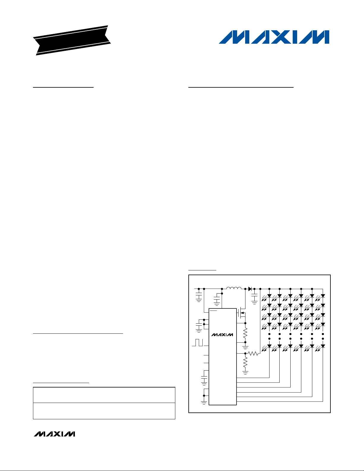
The MAX8790 is a high-efficiency driver for white lightemitting diodes (LEDs). It is designed for large liquidcrystal displays (LCDs) that employ an array of LEDs as
the light source. A current-mode step-up controller drives
up to six parallel strings of multiple series-connected
LEDs. Each string is terminated with ballast that achieves
±1.5% current regulation accuracy, ensuring even brightness for all LEDs. The MAX8790 has a wide input-voltage
range from 4.5V to 26V, and provides a fixed 20mA or
adjustable 15mA to 25mA full-scale LED current.
The MAX8790 has two dimming control modes to
enable a wide variety of applications. In direct DPWM
mode, the LED current is directly turned on and off by a
PWM signal. In analog dimming mode, an internal
phase-locked loop (PLL) circuit translates the PWM signal into an analog signal and linearly controls the LED
current down to 12.5%. Below 12.5%, digital dimming is
added to allow lower average LED current down to 1%.
Both control methods provide 100:1 dimming range.
The MAX8790 has multiple features to protect the controller from fault conditions. Separate feedback loops limit
the output voltage if one or more LEDs fail open or short.
The controller features cycle-by-cycle current limit to provide consistent operation and soft-start capability. A thermal-shutdown circuit provides another level of protection.
The step-up controller uses an external MOSFET, which
provides good efficiency and allows for scalable output
power and maximum operating voltage. Low feedback
voltage at each LED string (450mV) helps reduce
power loss. The MAX8790 features selectable switching
frequency (500kHz, 750kHz, or 1MHz), which allows
trade-offs between external component size and operating efficiency.
The MAX8790 is available in a thermally enhanced,
lead-free, 20-pin, 4mm x 4mm, Thin QFN package.
Applications
Notebook, Subnotebook, and Tablet Computer
Displays
Automotive Systems
Handy Terminals
Features
o Drives Six Parallel Strings with Multiple Series-
Connected LEDs per String
o ±1.5% Current Regulation Accuracy Between
Strings
o Low 450mV Feedback Voltage at Full Current
Improves Efficiency
o Step-Up Controller Regulates the Output Just
Above the Highest LED String Voltage
o Full-Scale LED Current Adjustable from 15mA to
25mA, or Preset 20mA
o Wide 100:1 Dimming Range
o Programmable Dimming Control: Direct DPWM or
Analog Dimming
o Built-In PLL for Synchronized Dimming Control
o Open and Short LED Protections
o Output Overvoltage Protection
o Wide Input Voltage Range from 4.5V to 26V
o External MOSFET Allows a Large Number of LEDs
per String
o 500kHz/750kHz/1MHz Switching Frequency
o Small, 20-Pin, 4mm x 4mm Thin QFN Package
MAX8790
Six-String White LED Driver with Active
Current Balancing for LCD Panel Applications
________________________________________________________________
Maxim Integrated Products
1
Simplified Operating Circuit
Ordering Information
19-0658; Rev 0; 11/06
For pricing, delivery, and ordering information, please contact Maxim/Dallas Direct! at
1-888-629-4642, or visit Maxim’s website at www.maxim-ic.com.
+
Denotes a lead-free package.
EVALUATION KIT
AVAILABLE
PART
TEMP RANGE
PIN-PACKAGE
PKG
CODE
MAX8790ETP+
20 Thin QFN
T2044-3
Pin Configuration appears at end of data sheet.
-40°C to +85°C
(4mm x 4mm)
V
D1
IN
MAX8790
GND
L1
EXT
CS
OV
FB1
FB2
FB3
FB4
FB5
FB6
V
IN
C
IN
0.1μF
SHDN
V
CC
FSET
ISET
BRT
N.C.
OSC
N.C.
CPLL
CCV
ENA
EP
OUT
N1
Rs
R1
R2
Page 2
ABSOLUTE MAXIMUM RATINGS
ELECTRICAL CHARACTERISTICS
(Circuit of Figure 1. VIN= 12V, V
SHDN
= VIN, CCV = 0.1µF, TA= 0°C to +85°C, unless otherwise noted. Typical values are at TA= +25°C.)
Stresses beyond those listed under “Absolute Maximum Ratings” may cause permanent damage to the device. These are stress ratings only, and functional
operation of the device at these or any other conditions beyond those indicated in the operational sections of the specifications is not implied. Exposure to
absolute maximum rating conditions for extended periods may affect device reliability.
IN, SHDN, to GND .................................................-0.3V to +28V
FB_ to GND ............................................................-0.3V to +28V
V
CC
, BRT, ENA, OSC, OV to GND ...........................-0.3V to +6V
ISET, CCV, CS, FSET, CPLL, EXT to GND .-0.3V to (V
CC
+ 0.3V)
Continuous Power Dissipation (T
A
= +70°C)
20-Pin Thin QFN (derate 16.9mW/°C above +70°C) ...1349mW
Operating Temperature Range ...........................-40°C to +85°C
Junction Temperature......................................................+150°C
Storage Temperature Range .............................-60°C to +150°C
Lead Temperature (soldering, 10s) .................................+300°C
MAX8790
Six-String White LED Driver with Active
Current Balancing for LCD Panel Applications
2 _______________________________________________________________________________________
PARAMETER CONDITIONS MIN TYP MAX UNITS
IN Input Voltage Range
IN Quiescent Current
VCC Output voltage V
VCC Short-Circuit Current 15 56 130 mA
VCC UVLO Threshold Rising edge, hysteresis = 20mV 4.00 4.25 4.45 V
STEP-UP CONVERTER
EXT High Level 10mA from EXT to GND
EXT Low Level -10mA from EXT to V
EXT On-Resistance EXT high or low 2 5 Ω
EXT Sink/Source Current EXT forced to 2V 1 A
OSC High-Level Threshold
OSC Midlevel Threshold 1.5
OSC Low-Level Threshold 0.4 V
Operating Frequency
Minimum Duty Cycle
Maximum Duty Cycle 94 95 %
CS Trip Voltage Duty cycle = 75% 85 100 115 mV
CONTROL INPUT
SHDN Logic-Input High Level 2.1 V
SHDN Logic-Input Low Level 0.8 V
BRT, ENA Logic-Input High Level 2.1 V
BRT, ENA Logic-Input Low Level 0.8 V
V
= V
IN
CC
V
= bypassed to GND through 1µF cap 5.5 26.0
CC
V
= high
SHDN
SHDN = GND
= 5V, 6V < VIN < 26V, 0 < I
SHDN
CC
V
= V
V
V
OSC
OSC
OSC
CC
= open 675 750 825
= GND 450 500 550
PWM mode 10
Pulse skipping, no load 0
4.5 5.5
VIN = 26V 1 2
= VCC = 5V 1 2
V
IN
10 µA
< 10mA 4.7 5.0 5.3 V
VCC
V
-
CC
0.1
V
CC
V
0 0.1 V
V
-
CC
0.4
V
VCC -
2.0
0.9 1.0 1.1 MHz
V
mA
V
kHz
%
Page 3
MAX8790
Six-String White LED Driver with Active
Current Balancing for LCD Panel Applications
_______________________________________________________________________________________ 3
ELECTRICAL CHARACTERISTICS (continued)
(Circuit of Figure 1. VIN= 12V, V
SHDN
= VIN, CCV = 0.1µF, TA= 0°C to +85°C, unless otherwise noted. Typical values are at TA= +25°C.)
PARAMETER CONDITIONS MIN TYP MAX UNITS
INPUT LEAKAGE
SHDN Leakage Current SHDN = 26V +35 µA
CS Leakage Current VCS = GND +40 +50 µA
OSC Leakage Current -3 +3 µA
BRT, ENA Leakage Current -1 +1 µA
FSET, ISET Leakage Current FSET = ISET = V
OV Leakage Current -0.1 +0.1 µA
LED CURRENT
Full-Scale FB_ Output Current
ISET High-Level Threshold Default setting for 20mA full-scale LED current
ISET Voltage 1.12 1.19 1.26 V
20% Output Current ISET = VCC, BRT = 20% 3.84 4.00 4.16 mA
Current Regulation Between
Strings
Minimum FB_ Regulation Voltage
Maximum FB_ Ripple ISET = V
FB_ On-Resistance V
FB_ Leakage Current
BRT Input Frequency 100 500 Hz
Minimum BRT Duty Cycle PLL active 12.5 %
FAULT PROTECTION
OV Threshold Voltage 1.16 1.23 1.30 V
FB_ Overvoltage Threshold
FAULT Shutdown Timer V
Thermal-Shutdown Threshold (Note 1) 170 °C
PHASE-LOCKED LOOP
FSET High-Level Threshold PLL disabled
BRT Frequency Capture Range
CC
ISET = V
R
ISET
R
ISET
ISET = V
ISET = V
R
ISET
ISET = V
ISET = V
FB_
SHDN = GND, V
SHDN = V
FB_
R
FSET
R
FSET
, BRT = 100% 19.40 20.00 20.60
CC
= 80kΩ to GND, BRT = 100% 24.25 25.00 25.75
= 133kΩ to GND, BRT = 100% 14.40 15.00 15.60
, BRT = 100% -1.5 +1.5 %
CC
, BRT = 20% -2.0 +2.0 %
CC
= 80kΩ to GND, BRT = 100% 300 500 800
, BRT = 100% 270 450 720
CC
, 12.5% 150 275 500
CC
CC , COUT
= 50mV 13 20 Ω
IN
> 5.6V (typ) 50 65 80 ms
= 500kΩ 150 200 250
= 250kΩ 300 400 500
= 1µF, OSC = VCC (Note 1) 120 200 mV
= 26V 1
FB_
, BRT = GND, V
FB_
= 15V
-1 +1 µA
V
-
CC
0.4
V
10 28
VCC +
0.20
V
CC
0.4
V
+
CC
0.6
-
V
V
1.45
CC
+
mA
mV
P-P
µA
V
Hz
Page 4
MAX8790
Six-String White LED Driver with Active
Current Balancing for LCD Panel Applications
4 _______________________________________________________________________________________
ELECTRICAL CHARACTERISTICS
(Circuit of Figure 1. VIN= 12V, V
SHDN
= VIN, CCV = 0.1µF, TA= -40°C to +85°C, unless otherwise noted.) (Note 2)
PARAMETER CONDITIONS MIN TYP MAX UNITS
IN Input Voltage Range
IN Quiescent Current
VCC Output Voltage V
VCC Short-Circuit Current 12 130 mA
VCC UVLO Threshold Rising edge, hysteresis = 20mV 4.00 4.45 V
STEP-UP CONVERTER
EXT High Level 10mA from EXT to GND
EXT Low Level -10mA from EXT to V
EXT On-Resistance EXT high or low 5 Ω
OSC High-Level Threshold
OSC Midlevel Threshold 1.5
OSC Low-Level Threshold 0.4 V
Maximum Duty Cycle 94 %
CS Trip Voltage Duty cycle = 75% 85 115 mV
CONTROL INPUT
SHDN Logic-Input High Level 2.1 V
SHDN Logic-Input Low Level 0.8 V
BRT, ENA Logic-Input High Level 2.1 V
BRT, ENA Logic-Input Low Level 0.8 V
INPUT LEAKAGE
SHDN Leakage Current SHDN = 26V +35 µA
CS Leakage Current VCS = GND +50 µA
OSC Leakage Current -3 +3 µA
BRT, ENA Leakage Current -1 +1 µA
FSET, ISET Leakage Current FSET = ISET = V
OV Leakage Current -0.1 +0.1 µA
V
= V
IN
CC
V
bypassed to GND through 1µF cap 5.5 26.0
CC
V
= high
SHDN
SHDN = GND
= 5V, 6V < VIN < 26V, 0 < I
SHDN
V
= V
V
V
OSC
OSC
OSC
CC
= open 675 825Operating Frequency
= GND 450 550
VIN = 26V 2
= VCC = 5V 2
V
IN
< 10mA 4.7 5.3 V
VCC
CC
CC
4.5 5.5
V
CC
0.1
V
CC
0.4
0.9 1.1 MHz
-1 +1 µA
10 µA
-
V
0.1 V
-
V
VCC -
2.0
V
mA
V
kHz
Page 5
MAX8790
Six-String White LED Driver with Active
Current Balancing for LCD Panel Applications
_______________________________________________________________________________________ 5
Note 1: Specifications are guaranteed by design, not production tested.
Note 2: Specifications to -40°C are guaranteed by design, not production tested.
ELECTRICAL CHARACTERISTICS (continued)
(Circuit of Figure 1. VIN= 12V, V
SHDN
= VIN, CCV = 0.1µF, TA= -40°C to +85°C, unless otherwise noted.) (Note 2)
PARAMETER CONDITIONS MIN TYP MAX UNITS
LED CURRENT
ISET High-Level Threshold Default setting for 20mA full-scale LED current
ISET Voltage 1.12 1.26 V
20% Output Current ISET = VCC, BRT = 20% 3.8 4.2 mA
Current Regulation Between
Strings
Maximum FB_ Ripple ISET= VCC, C
FB_ On-Resistance V
FB_ Leakage Current
BRT Input Frequency 100 500 Hz
FAULT PROTECTION
OV Threshold Voltage 1.16 1.30 V
FB_ Overvoltage Threshold
FAULT Shutdown Timer V
ISET = V
R
ISET
R
ISET
ISET = V
ISET = V
R
ISET
ISET= V
ISET = V
FB_
SHDN = GND, V
SHDN = V
FB_
, BRT = 100% 19.2 20.8
CC
= 80kΩ to GND, BRT = 100% 24.0 26.0Full-Scale FB_ Output Current
= 133kΩ to GND, BRT = 100% 14.4 15.6
V
CC
0.4
, BRT = 100% -2 +2
CC
, BRT = 20% -3 +3
CC
= 80kΩ to GND, BRT = 100% 280 840
, BRT = 100% 250 760Minimum FB_ Regulation Voltage
CC
, BRT = 12.5% 140 530
CC
= 1µF, OSC = VCC (Note 1) 200 mV
OUT
= 50mV 20 Ω
= 26V 1
FB_
, BRT = GND, V
IN
> 5.6V (typ) 50 80 ms
= 15V 28
FB_
V
CC
0.2
-
V
+
VCC +
1.45
PHASE-LOCKED LOOP
V
-
FSET High-Level Threshold PLL disabled
R
= 500kΩ 150 250 Hz
BRT Frequency Capture Range
FSET
R
= 250kΩ 300 500 Hz
FSET
CC
0.4
V
mA
%
mV
P-P
µA
V
Page 6
MAX8790
Six-String White LED Driver with Active
Current Balancing for LCD Panel Applications
6 _______________________________________________________________________________________
Typical Operating Characteristics
(Circuit configuration 1, VIN= 12V, V
SHDN
= VIN, LEDs = 8 series x 6 parallel strings, ISET = VCC, TA= +25°C, unless otherwise noted.)
BOOST CONVERTER EFFICIENCY
vs. INPUT VOLTAGE (BRT = 100%)
MAX8790 toc01
BOOST CONVERTER EFFICIENCY (%)
INPUT VOLTAGE (V)
94
93
92
91
90
89
88
87
86
71217
500kHz
750kHz
1MHz
NORMALIZED POWER vs. TOTAL LED CURRENT
(ANALOG AND DPWM DIMMING)
MAX8790 toc02
NORMALIZED POWER
TOTAL LED CURRENT (mA)
1.2
1.0
0.8
0.6
0.4
0.2
0
1 10 100 1000
NORMALIZED TO VIN = 20V, AND I
LED
= 20mA
V
IN
= 7V
TOTAL LED
POWER, ANALOG
TOTAL INPUT
POWER, DPWM
TOTAL INPUT
POWER, ANALOG
TOTAL LED
POWER, DPWM
LED CURRENT vs. BRT DUTY CYCLE
(BRT AT 200Hz)
MAX8790 toc03
LED CURRENT (mA)
BRT DUTY CYCLE (%)
25
20
15
10
5
0
1 10 100
IDENTICAL FOR DPWM DIMMING
AND ANALOG DIMMING
LED CURRENT
vs. AMBIENT TEMPERATURE (BRT = 100%)
MAX8790 toc04
LED CURRENT (mA)
AMBIENT TEMPERATURE (°)
21.0
20.8
20.6
20.4
20.2
20.0
19.8
19.6
19.4
19.2
19.0
020 6040 80
LED CURRENT REGULATION
vs. INPUT VOLTAGE
MAX8790 toc05
LED CURRENT REGULATION (%)
INPUT VOLTAGE (V)
0.05
0.04
0.03
0.02
0.01
0
-0.01
-0.02
-0.03
-0.04
-0.05
71217
ANALOG DIMMING
BRT = 10%
DPWM DIMMING
BRT = 100%
DPWM DIMMING
BRT = 10%
FB_ VOLTAGE vs. LED CURRENT
(ANALOG DIMMING)
MAX8790 toc06
FB_ REGULATION VOLTAGE (V)
LED STRING CURRENT (mA)
0.7
0.6
0.5
0.4
0.3
0.2
0.1
0
0 5 10 15 20 25 30
SUPPLY CURRENT vs. INPUT VOLTAGE
(DPWM DIMMING)
MAX8790 toc07
SUPPLY CURRENT (mA)
INPUT VOLTAGE (V)
7
6
5
4
3
2
1
0
71217
BRT = 100%
BRT = 0%
SHUTDOWN CURRENT vs. INPUT VOLTAGE
MAX8790 toc08
SHUTDOWN CURRENT (μA)
INPUT VOLTAGE (V)
7
6
5
4
3
2
1
0
71217
SWITCHING WAVEFORMS
(BRT = 100%)
MAX8790 toc09
200ns/div
I
L
500mA/div
0mA
V
LX
10V/div
0V
Page 7
MAX8790
Six-String White LED Driver with Active
Current Balancing for LCD Panel Applications
_______________________________________________________________________________________
7
Typical Operating Characteristics (continued)
(Circuit configuration 1, VIN= 12V, V
SHDN
= VIN, LEDs = 8 series x 6 parallel strings, ISET = VCC, TA= +25°C, unless otherwise noted.)
SWITCHING WAVEFORMS
(BRT = 15%, ANALOG DIMMING)
1μs/div
MAX8790 toc10
LED CURRENT WAVEFORMS
(BRT = 1% AT 200Hz, DPWM DIMMING)
LED CURRENT WAVEFORMS
(BRT = 50% AT 200Hz, DPWM DIMMING)
2ms/div
MAX8790 toc14
MAX8790 toc12
0V
0V
V
LX
10V/div
0V
I
L
500mA/div
0mA
STARTUP WAVEFORMS
(BRT = 100%, DPWM DIMMING)
4ms/div
MAX8790 toc13
BRT
5V/div
0V
V
FB1
5V/div
0V
MAX8790 toc11
SHDN
5V/div
0V
V
OUT
20V/div
0V
V
CCV
2V/div
0V
I
L
1A/div
0A
LED CURRENT WAVEFORMS
(BRT = 50% AT 200Hz, ANALOG DIMMING)
BRT
5V/div
V
FB1
1V/div
0V
0V
0mA
0A
BRT
5V/div
V
FB1
5V/div
I
LED
100mA/div
I
L
1A/div
1ms/div
LED CURRENT WAVEFORMS
(BRT = 1% AT 200Hz, ANALOG DIMMING)
1ms/div
MAX8790 toc15
0mA
0A
0V
0V
0mA
0mA
I
LED
100mA/div
I
L
1A/div
BRT
5V/div
V
FB1
2V/div
I
LED
50mA/div
I
L
500mA/div
1ms/div
LED-OPEN FAULT PROTECTION
(BRT = 100%, LED OPEN ON FB3)
20ms/div
MAX8790 toc16
0mA
0A
0V
0V
0V
0A
I
LED
50mA/div
I
L
1A/div
V
FB3
1V/div
V
FB1
10V/div
V
OUT
20V/div
I
L
1A/div
Page 8
MAX8790
Six-String White LED Driver with Active
Current Balancing for LCD Panel Applications
8 _______________________________________________________________________________________
Typical Operating Characteristics (continued)
(Circuit configuration 1, VIN= 12V, V
SHDN
= VIN, LEDs = 8 series x 6 parallel strings, ISET = VCC, TA= +25°C, unless otherwise noted.)
LED-SHORT FAULT PROTECTION
(BRT = 100%, 2 LEDs SHORT ON FB3)
10ms/div
0A
V
FB3
1V/div
V
FB1
10V/div
V
OUT
20V/div
I
L
1A/div
0V
0V
0V
MAX8790 toc17
LED CURRENT BALANCING
vs. INPUT VOLTAGE (BRT = 100%)
MAX8790 toc18
LED CURRENT BALANCING ACCURACY (%)
INPUT VOLTAGE (V)
1.00
0.90
0.80
0.70
0.60
0.50
0.40
0.30
0.20
0.10
0
71217
750kHz
500kHz
1MHz
Pin Description
PIN NAME FUNCTION
1 OSC
2 ENA
3 BRT
4 SHDN
5 FB1
6 FB2
7 FB3
8 GND Ground
9 FB4
10 FB5
O sci l l ator Fr eq uency S el ecti on P i n. C onnect OS C to V
1M H z. C onnect O S C to G N D to set the fr eq uency to 500kH z. Fl oat OS C to set the fr eq uency to 750kH z.
Anal og D i m m i ng E nab l e. E N A sets the P WM contr ol m od e. S et E N A LOW to enab l e d i r ect D P WM d i m m i ng .
S et E N A H IGH to enab l e anal og d i m m i ng . In b oth m od es, the d uty cycl e of the P WM si g nal at the BRT i np ut
contr ol s the LE D cur r ent char acter i sti cs. S ee the D i m m i ng C ontr ol secti on for a com p l ete d escr i p ti on.
Brightness Control Input. The duty cycle of this digital input signal controls the LED current characteristics.
The allowable frequency range is 100Hz to 500Hz in analog dimming mode. The duty cycle can be 100%
to 1%. The BRT frequency can go above 500Hz in direct DPWM mode as long as the BRT pulse width is
greater than 50µs minimum. See the Dimming Control section for a complete description.
Shutdown Control Input. The MAX8790 shuts down when SHDN is less than 0.8V. Pulling SHDN above
2.1V enables the MAX8790. SHDN can be connected to the input voltage if desired.
LED String 1 Cathode Connection. FB1 is the open-drain output of an internal regulator, which controls
current through FB1. FB1 can sink up to 25mA. If unused, connect FB1 to GND.
LED String 2 Cathode Connection. FB2 is the open-drain output of an internal regulator, which controls
current through FB2. FB2 can sink up to 25mA. If unused, connect FB2 to GND.
LED String 3 Cathode Connection. FB3 is the open-drain output of an internal regulator, which controls
current through FB3. FB3 can sink up to 25mA. If unused, connect FB3 to GND.
LED String 4 Cathode Connection. FB4 is the open-drain output of an internal regulator, which controls
current through FB4. FB4 can sink up to 25mA. If unused, connect FB4 to GND.
LED String 5 Cathode Connection. FB5 is the open-drain output of an internal regulator, which controls
current through FB5. FB5 can sink up to 25mA. If unused, connect FB5 to GND.
to set the step - up conver ter ’ s osci l l ator fr eq uency to
C C
Page 9

MAX8790
Six-String White LED Driver with Active
Current Balancing for LCD Panel Applications
_______________________________________________________________________________________ 9
Pin Description (continued)
PIN NAME FUNCTION
11 FB6
12 CS
13 EXT External MOSFET Gate-Drive Output
14 OV
15 V
16 IN
17 CCV
18 ISET
19 FSET
20 CPLL
EP EP
CC
LED String 6 Cathode Connection. FB6 is the open-drain output of an internal regulator, which controls
current through FB6. FB6 can sink up to 25mA. If unused, connect FB6 to GND.
Step-Up Controller Current-Sense Input. Connect the CS input to a ground-referenced sense resistor to
measure the current in the external MOSFET switch.
Overvoltage Sense. Connect OV to the center tap of a resistive voltage-divider from V
detection threshold for voltage limiting at OV is 1.23V (typ).
5V Linear Regulator Output. VCC provides power to the MAX8790 and is also used to bias the gate driver
for the external MOSFET. Bypass V
than or equal to 5.5V, connect V
V
. When SHDN is low, the internal linear regulator is disabled.
CC
Supply Input. V
at the pin with a 0.1µF or greater ceramic capacitor.
Step-Up Converter Compensation Pin. Connect a 0.1µF ceramic capacitor and 1.2kΩ resistor from CCV to
GND. When the MAX8790 shuts down, CCV is discharged to 0V through an internal 20kΩ resistor.
Full-Scale LED Current Adjustment Pin. The resistance from ISET to GND controls the full-scale current in
each LED string:
The acceptable resistance range is 80kΩ < R
25mA > I
PLL Free-Running Frequency Control Pin. The resistance from FSET to GND controls the PLL oscillator’s
free-running frequency, f
The capture range is 0.6 x f
754kΩ, which corresponds to a frequency range of 500Hz > f
frequency range is 100Hz to 500Hz.
Phase-Locked Loop-Compensation Capacitor Pin. The capacitance at CPLL compensates the PLL loop
response. Connect a 0.1µF ceramic capacitor from CPLL to GND.
Exposed Backside Pad. Solder to the circuit board ground plane with sufficient copper connection to
ensure low thermal resistance. See the PCB Layout Guidelines section.
LEDmax
biases the internal 5V linear regulator that powers the device. Bypass IN to GND directly
IN
> 15mA. Connect ISET to VCC for a default full-scale LED current of 20mA.
:
PLL
PLL
to GND with a ceramic capacitor of 1µF or greater. If VIN is less
CC
to IN to the disable the internal LDO and use the external 5V supply to
CC
I
to f
. The acceptable resistance range for FSET is 250kΩ < R
PLL
= 20mA x 100kΩ/R
LEDmax
ISET
f
= 1 / (10 x R
PLL
< 133kΩ, which corresponds to full-scale LED current of
FSET
ISET
x 800pF)
> 166Hz. The resulting capture
PLL
to ground. The
OUT
FSET
<
Page 10

MAX8790
Detailed Description
The MAX8790 is a high-efficiency driver for arrays of
white LEDs. It contains a fixed-frequency, currentmode, PWM step-up controller, 5V linear regulator, dimming control circuit, and six regulated current sources
(see Figure 2). When enabled, the step-up controller
boosts the output voltage to provide sufficient headroom for the current sources to regulate their respective
string currents. The MAX8790 features selectable
switching frequency (500kHz, 750kHz, or 1MHz), which
allows trade-offs between external component size and
operating efficiency. The control architecture automatically skips pulses at light loads to improve efficiency
and prevents overcharging the output capacitor.
A PWM logic input signal, BRT, controls the LED brightness. The MAX8790 supports both analog and digital
control of the LED current, and achieves 100:1 dimming
range. The MAX8790’s dimming control circuit consists
of a PLL, a digital comparator, and a DAC. In direct
DPWM mode, the step-up controller and current source
are directly turned on and off by the PWM signal. In analog dimming mode, an internal PLL, digital comparator,
and DAC circuit translate the PWM signal into an analog
signal that linearly controls the LED current, down to a
PWM duty factor of 12.5%.
The MAX8790 has multiple features to protect the controller from fault conditions. Separate feedback loops
limit the output voltage if one or more LEDs fail open or
short. During operation, if one of the feedback string
voltages exceeds the V
CC
to 0.6V (typ) protection
threshold, the controller shuts down and latches off
after an internal timer expires. The controller features
cycle-by-cycle current limit to provide consistent operation and soft-start capability. A thermal-shutdown circuit
provides another level of protection.
The MAX8790 includes a 5V linear regulator that provides the internal bias and gate drive for the step-up
controller. When an external 5V is available, the internal
LDO can be overdriven to decrease power dissipation.
Otherwise, connect the IN pin to an input greater than
5.5V. The internal LDO is disabled when SHDN is low.
Six-String White LED Driver with Active
Current Balancing for LCD Panel Applications
10 ______________________________________________________________________________________
Figure 1. Typical Operating Circuit
V
IN
7V TO 21V
C
IN
0.1μF
L1
4.7μH
V
D1
C
OUT
OUT
UP TO 35V
IN
MAX8790
EXT
GND
FB1
FB2
FB3
FB4
FB5
FB6
N1
CS
R
S
56mΩ
R1
R2
37.4kΩ
1MΩ
OV
1μF
511kΩ
SHDN
V
CC
ENA
ISET
BRT
FSET
N.C.
1.2kΩ
0.1μF
0.1μF
OSC
CCV
CPLL
EP
Page 11

MAX8790
Six-String White LED Driver with Active
Current Balancing for LCD Panel Applications
______________________________________________________________________________________ 11
Figure 2. Control Circuit Block Diagram
V
OSC
SHDN
CCV
ISET
FSET
OUTPUT OVERVOLTAGE
COMPARATOR
IN
CC
V
- 0.4V
CC
5V LINEAR
REGULATOR
V
CC
OSCILLATOR
TRI-LEVEL
COMPARATOR
REF ADJ
OSC
256 x f
BRT
CLK
SLOPE
COMPENSATION
65ms TIMER
SHUTDOWN
LATCH
ERROR
AMPLIFIER
REF
8-BIT DAC
8
DIGITAL CONTROL
CLOCK
FB OVERVOLTAGE
COMPARATOR
gm
SAT
ERROR
COMPARATOR
+ 0.6V
V
CC
CONTROL AND
DRIVER LOGIC
CURRENT SENSE
HVC
LVC
EN
CURRENT SOURCE
1.25V
OV
EXT
CS
FB6
FB5
FB4
FB3
FB2
FB1
N
10Ω
GND
CPLL
BRT
ENA
PLL
8-BIT
COUNTER
5 MSBs
8
LATCH
5 LSBs
DIGITAL
COMPARATOR
8-BIT
8
CURRENT SOURCE
CURRENT SOURCE
CURRENT SOURCE
CURRENT SOURCE
CURRENT SOURCE
FB2
FB3
FB4
FB5
FB6
Page 12

MAX8790
Fixed-Frequency Step-Up Controller
The MAX8790’s fixed-frequency, current-mode, step-up
controller automatically chooses the lowest active FB_
voltage to regulate the feedback voltage. Specifically,
the difference between the lowest FB_ voltage and the
current source-control signal plus an offset (V
SAT
) is
integrated at the CCV output. The resulting error signal
is compared to the external switch current plus slope
compensation to terminate the switch on-time. As the
load changes, the error amplifier sources or sinks current to the CCV output to adjust the required peak
inductor current. The slope-compensation signal is
added to the current-sense signal to improve stability at
high duty cycles.
At light loads, the MAX8790 automatically skips pulses
to improve efficiency and prevent overcharging the output capacitor. In SKIP mode, the inductor current ramps
up for a minimum on-time of approximately 150ns, then
discharges the stored energy to the output. The switch
remains off until another pulse is needed to boost the
output voltage.
Internal 5V Linear Regulator
V
CC
and UVLO
The MAX8790 includes an internal low-dropout linear
regulator (VCC). When VINis higher than 5.5V and
SHDN is high, this linear regulator generates a 5V supply to power an internal PWM controller, control logic,
and MOSFET driver. This linear regulator can deliver at
least 10mA of total additional load current. If VINis less
than or equal to 5.5V, VCCand IN can be connected
together and powered from an external 5V supply.
There is an internal diode from VCCto IN, so VINmust
be greater than VCC(see Figure 2).
The MAX8790 includes UVLO protection. The controller
is disabled until VCCexceeds the UVLO threshold of
4.25V (typ). Hysteresis on UVLO is approximately 20mV.
The V
CC
pin should be bypassed to GND with a 1µF or
greater ceramic capacitor.
Six-String White LED Driver with Active
Current Balancing for LCD Panel Applications
12 ______________________________________________________________________________________
Figure 3. Low-Input-Voltage Application Circuit
V
IN
2.8V TO 5.5V
C
IN
L1
0.9μH
D1
C
OUT
V
OUT
UP TO 22V
IN
MAX8790
EXT
GND
FB1
FB2
FB3
FB4
FB5
FB6
N1
CS
R
S
30mΩ
R1
R2
59kΩ
1MΩ
OV
EXTERNAL
5V SUPPLY
511kΩ
SHDN
V
CC
1μF
N.C.
1.2kΩ
0.1μF
0.1μF
ENA
ISET
BRT
FSET
OSC
CCV
CPLL
EP
Page 13

Startup
At startup, the MAX8790 checks each FB_ pin to determine if the respective current string is enabled. Each
FB_ pin is internally pulled up with a 10µA current
source. If an FB_ pin is connected to GND, the corresponding string current source is disabled. This feedback scan takes approximately 264µs, after which the
step-up converter begins switching.
Shutdown
When the SHDN pin is less than 0.8V, the MAX8790
shuts down the internal LDO, the reference, current
sources, and all control circuitry. The resulting supply
current is less than 10µA. While the n-channel MOSFET
is turned off, the step-up regulator’s output is connected
to IN through the external inductor and rectifier diode.
Frequency Selection
A tri-level OSC input sets the internal oscillator frequency
for the step-up converter, as shown in Table 1. High-frequency (1MHz) operation optimizes the regulator for the
smallest component size, at the expense of efficiency
due to increased switching losses. Low-frequency
(500kHz) operation offers the best overall efficiency, but
requires larger components and PCB area.
Overvoltage Protection
To protect the step-up converter when the load is open,
or the output voltage becomes excessive for any reason, the MAX8790 features a dedicated overvoltage
feedback input (OV). The OV pin is connected to the
center tap of a resistive voltage-divider from the highvoltage output (see Figure 1). When the MAX8790 is
powered up, if none of the LED strings on FB1–FB6 are
connected to the step-up converter output, the step-up
converter regulates the output voltage to V
OUT
=
1.23V(1 + R1 / R2). When VOVexceeds 1.23V, a comparator turns off N1. The step-up converter switch is
reenabled after the output voltage drops below the protection threshold.
LED Current Sources
Maintaining uniform LED brightness and dimming
capability are critical for LCD backlight applications.
The MAX8790 is equipped with a bank of six matched
current sources. These specialized current sources are
accurate to within ±1.5% and can be switched on and
off within 10µs, enabling PWM frequencies of up to
2kHz. All LED full-scale currents are identical and are
set through the ISET pin (15mA < I
LED
< 25mA).
The minimum voltage drop across each current source
is approximately 450mV at 20mA. The low voltage drop
helps reduce dissipation while maintaining sufficient
compliance to control the LED current within the
required tolerances.
The LED current sources can be disabled by grounding
the respective FB_ pin at startup. When the IC is powered up, the controller scans settings for all FB_ pins. If
an FB_ pin is not grounded, an internal circuit pulls this
pin high, and the controller enables the corresponding
current source to regulate the string current. If the FB_ pin
is grounded, the controller disables the corresponding
current regulator. The current regulator cannot be disabled by grounding any of the FB_ pins after the IC is
powered up.
All FB_ pins in use are measured and the highest signal
(HVC) and the lowest signal (LVC) are extracted for two
feedback loops. HVC is used to identify excessive dissipation across the current-source inputs. When HVC is
greater than V
CC
+ 0.6V (typ) for greater than 65ms
(see the
Current-Source Fault Protection
section), a
fault latch is set and the MAX8790 is shut down. The
LDO output is not affected by the fault latch. LVC is fed
into the step-up converter’s error amplifier to regulate
the step-up converter’s output voltage.
Current-Source Fault Protection
The LED current sources are protected against string
open, short, and gross mismatch faults, using overvoltage detection circuitry on each FB_ pin. If any of these
three fault conditions persists for a preset duration, the
MAX8790 is latched off. The duration of the fault time
depends on the dimming mode and the duty cycle of
the BRT input (D
BRT
). In the DPWM mode, the timeout
interval is:
t
TIMEOUT_DPWM
= 65ms/D
BRT
In analog dimming mode, the fault time is fixed at 65ms
for D
BRT
greater than 12.5%. When D
BRT
is less than
12.5%, the timeout interval is:
t
TIMEOUT_ANALOG
= 8.125ms/D
BRT
The fault latch can be cleared by cycling the power or
toggling the shutdown pin SHDN.
Open-Current Source Protection
The MAX8790 step-up converter output voltage is regulated according to the minimum value of the enable FB_
voltages. If an individual LED string is open, the respective FB_ is pulled down to near ground. In this situation,
the step-up converter output voltage increases but is
MAX8790
Six-String White LED Driver with Active
Current Balancing for LCD Panel Applications
______________________________________________________________________________________ 13
Table 1. Frequency Selection
OSC SWITCHING FREQUENCY (kHz)
GND 500
Open 750
V
CC
1000
Page 14

MAX8790
clamped to a level set with the OV feedback input.
When this elevated output voltage is applied to the
undamaged strings, excessive voltage drop develops
across the FB_ pins. If the resulting HVC signal
exceeds V
CC
+ 0.6V for greater than 65ms, the fault
latch is triggered to protect the circuit.
LED-Short and String Mismatch Protection
Normally, white LEDs have variations in forward-voltage
drop of 3.1V to 3.6V. The MAX8790 can tolerate slight
mismatches between LED strings. When the sum of the
LED forward voltages creates a mismatch in the strings
so the HVC signal exceeds VCC+ 0.6V for greater than
65ms, the fault latch is triggered in much the same way
as the circuit responds to open string faults. Similar protection is activated when an LED is shorted.
The larger the number of series-connected LEDs (N),
the smaller the tolerable mismatch between LEDs:
V
SAT
≈ 450mV and VCC= 5V
For N = 8, the average error per LED = 644mV.
For N = 10, the average error per LED = 510mV.
The larger the total mismatch, the larger the voltage
drop required across each current source to correct for
the error, and therefore the larger the dissipation within
the MAX8790.
Dimming Control
The MAX8790 features both analog and digital dimming control. Analog dimming can provide potentially
higher converter efficiency because of low voltage drop
across each WLED when the current is low. Digital dimming (DPWM) provides less WLED color distortion
since the WLED current is held at full scale when the
WLED is on.
The MAX8790’s dimming control circuit consists of a
PLL, a digital comparator, and a DAC. The controller
provides 100:1 dimming range through either analog or
digital control methods. Both methods translate the
duty cycle of the BRT input into a control signal for the
LED current sources. In analog dimming mode, the current-source outputs are DC and the BRT duty cycle
(12.5% < D
BRT
< 100%) modulates the amplitude of
the currents. For D
BRT
< 12.5%, the LED current is digitally modulated to reduce the average LED current
down to 1% of full scale. The PLL detects the BRT frequency and phase, and adjusts the current-source
amplitude and duty cycle synchronously (see Figure 4).
Six-String White LED Driver with Active
Current Balancing for LCD Panel Applications
14 ______________________________________________________________________________________
Figure 4. LED Current Control Using Analog Dimming Mode
Error V V V
∑
N
Average Error Per LED
<+ −06.
CC SAT
Error V
∑
N
< 5 150.
=
5 150.
N
V
t
ON
D =
t
BRT
D = 50%
t
BRT
I
LEDMAX
I
LED
0A
ON
t
BRT
D = 30%
ANALOG DIMMING MODE
D = 12.5%
D = 6.25%
Page 15

In digital dimming mode, the step-up controller and
current source are directly turned on and off by the
PWM signal. The current pulse magnitude, or full-scale
current, is set by ISET and is independent of PWM duty
factor. The current-source outputs are PWM signals
synchronized to the BRT input signal (see Figure 5).
The full-scale current in both methods is specified by
resistance from the ISET pin to ground:
The acceptable resistance range is 80kΩ < R
ISET
<
133kΩ, which corresponds to full-scale LED current of
25mA > I
LEDmax
> 15mA. Connect ISET to VCCfor a
default full-scale LED current of 20mA. When ENA is
high, the analog dimming is enabled, when ENA is low,
digital dimming is enabled.
When the current-source output is pulse-width modulated,
current-source turn-on is synchronized with the BRT signal. Synchronization and low jitter in the PWM signals help
reduce flicker noise in the display. The current through
each FB_ pin is controlled only during the step-up converter’s on-time. During the converter’s off-time, the current sources are turned off. The output voltage does not
discharge and stays high. Each FB_ pin can withstand
28V, which is the pin’s maximum rated voltage.
Table 2 summarizes the characteristics of both analog
and digital dimming methods.
A PLL translates the duty cycle of the BRT input into a
reference for the MAX8790’s current sources. A resistor
from the FSET pin to ground controls the PLL’s freerunning frequency:
The PLL’s loop filter bandwidth is set with a capacitor
from the CPLL pin to ground. This filter integrates the
phase difference between the BRT input signal and the
PLL oscillator. The filter bandwidth determines the
PLL’s dynamic response to frequency changes in the
BRT signal. For most applications, a 0.1µF capacitor is
MAX8790
Six-String White LED Driver with Active
Current Balancing for LCD Panel Applications
______________________________________________________________________________________ 15
Figure 5. LED Current Control Using DPWM Dimming Mode
Table 2. Dimming Mode
mA k
I
LED
max
=
×20 100 Ω
R
ISET
D =
BRT
t
ON
t
BRT
D = 50%
t
ON
D = 30%
DPWM DIMMING MODE
f
=
PLL
10 800
1
RpF
××
FSET
D = 12.5%
D = 6.25%
t
BRT
I
LEDMAX
I
LED
0A
MODE ENA PLL FREQUENCY CPLL DESCRIPTION
Analog dimming from 100% to 12.5% brightness. From
Analog + DPWM > 2.1V 250kΩ < R
Direct DPWM < 0.8V V
FSET
> V
CC
< 754kΩ 0.1µF
FSET
- 0.4V, disables PLL OPEN
12.5% to 1% brightness, DPWM dimming is employed.
BRT frequency range is 100Hz to 500Hz.
Direct dimming by BRT signal. BRT frequency can be
100Hz to 2kHz; 50µs minimum BRT on-time limits the
minimum brightness.
Page 16

MAX8790
adequate for oscillator frequencies in the 166Hz < f
PLL
< 500Hz range. The PLL frequency capture window is
0.6 x f
PLL
to f
PLL
.
The PLL is disabled in DPWM mode; consequently, the
BRT frequency is not limited by f
PLL
. The maximum
BRT frequency is determined by the minimum BRT ontime of 50µs and the minimum acceptable dimming
factor. If a 1% dimming factor is needed, the maximum
BRT frequency is 200Hz. If a 10% dimming factor is
acceptable, the maximum BRT frequency is 2kHz.
In analog dimming mode, load-current transients can
occur when the BRT duty cycle abruptly changes on
the fly. Large regulation transients induce a flash on the
LED load that is observable with the naked eye and
should therefore be avoided. Such annoying flashes
can be eliminated by dynamically changing the ENA
pin setting. When a capacitor is connected to the CPLL
pin and the ENA pin is grounded, the PLL continues to
run but does not affect the dimming. When fast PLL
lockup transitions are required, the ENA pin can be
momentarily pulled to ground; after the PLL is locked
up, ENA can be pulled high to reenable PLL in dimming control.
Thermal Shutdown
The MAX8790 includes a thermal-protection circuit.
When the local IC temperature exceeds +170°C (typ),
the controller and current sources shut down and do
not restart until the die temperature drops by 15°C.
Design Procedure
All MAX8790 designs should be prototyped and tested
prior to production. Table 3 provides a list of power
Six-String White LED Driver with Active
Current Balancing for LCD Panel Applications
16 ______________________________________________________________________________________
Table 3. Component List
CIRCUIT FIGURE 1 FIGURE 1 FIGURE 1 FIGURE 3
Switching
Frequency
White LED
Number of
White LEDs
Input Voltage 4.5V to 5.5V, VCC = IN 7V to 21V 7V to 21V 2.8V to 5.5V, VCC = 5V
Inductor L1
Input
Capacitors
C
Output
OUT
Capacitor
MOSFET N1
Diode
Rectifier D1
Sense
Resistor
1MHz 750kHz 500kHz 750kHz
3.2V (typ), 3.5V (max) at
20mA
Nichia NSSW008C
6 series x 6 parallel,
20mA (max)
2.2µH , 2.5A p ow er i nd uctor
Sumida CDRH5D16-2R2
10µF ±10%, 10V X5R
ceramic capacitor (1206)
Murata GRM31MR61A106K
2.2µF ±10%, 50V X7R
ceramic capacitor (1x)
Murata GRM31CR71H225K
30V, 3A n-channel MOSFET
(6-pin SC70)
Vishay Si1402DH
2A, 30V Schottky diode
Nihon EC21QS03L
50mΩ ±1%, 1/2W
IRC LRC-LRF-1206LF-01R050-F
3.2V (typ), 3.5V (max) at
20mA
Nichia NSSW008C
8 series x 6 parallel,
20mA (max)
4.7µH , 2.05A p ow er i nd uctor
Sumida CDRH5D16-4R7
10µF ±10%, 25V X5R
ceramic capacitor (1206)
M ur ata GRM 31C R61E 106KA
2.2µF ±10%, 50V X7R
ceramic capacitor (1206)
(1x)
Murata GRM31CR71H225K
60V, 2.8A n-channel
MOSFET (6-pin TSOP)
Fairchild Semiconductor
FDC5612
Sanyo Semiconductor
CPH6424
2A, 40V Schottky diode
Toshiba CMS11
Nihon EC21QS04
56mΩ ±1%, 1/2W
IRC LRC-LRF-1206LF-01R056-F
3.2V (typ), 3.5V (max) at
20mA
Nichia NSSW008C
10 series x 6 parallel,
25mA (max)
4.7µH , 3.6A p ow er i nd uctor
Sumida CDRH8D28-4R7
10µF ±10%, 25V X5R
ceramic capacitor (1206)
M ur ata GRM 31C R61E 106KA
4.7µF ±10%, 50V X7R
ceramic capacitor (1210)
(1x)
Murata GRM32ER71H475K
60V , 6A n- channel M O S FE T
( P ow er P AK 1212- 8)
Vishay Si7308DN
3A, 60V Schottky diode
Nihon EC31QS06
40mΩ ±1%, 1/2W
IRC LRC-LRF-1206LF-01R040-F
3.2V (typ), 3.5V (max) at
20mA
Nichia NSSW008C
6 series x 6 parallel,
20mA (max)
0.9µH , 4.7A p ow er i nd uctor
Sumida CDRH5D16-0R9
10µF ±10%, 10V X5R
ceramic capacitor (1206)
M ur ata GRM 31M R61A106K
2.2µF ±10%, 50V X7R
ceramic capacitor (1x)
Murata GRM31CR71H225K
30V, 4.9A n-channel
MOSFET (6-pin TSOP)
Vishay Si3456BDV
3A, 30V Schottky diode
Nihon EC31QS03L
30mΩ ±1%, 1/2W
IRC LRC-LRF-1206LF-01R030-F
Page 17

components for the typical applications circuit. Table 4
lists component suppliers. External component value
choice is primarily dictated by the output voltage and the
maximum load current, as well as maximum and minimum
input voltages. Begin by selecting an inductor value.
Once L is known, choose the diode and capacitors.
Inductor Selection
The inductance, peak current rating, series resistance,
and physical size should all be considered when
selecting an inductor. These factors affect the converter’s operating mode, efficiency, maximum output load
capability, transient response time, output voltage ripple,
and cost.
The maximum output current, input voltage, output voltage, and switching frequency determine the inductor
value. Very high inductance minimizes the current ripple, and therefore reduces the peak current, which
decreases core losses in the inductor and I
2
R losses in
the entire power path. However, large inductor values
also require more energy storage and more turns of
wire, which increases physical size and I2R copper
losses in the inductor. Low inductor values decrease
the physical size, but increase the current ripple and
peak current. Finding the best inductor involves the
compromises among circuit efficiency, inductor size,
and cost.
When choosing an inductor, the first step is to determine the operating mode: continuous conduction mode
(CCM) or discontinuous conduction mode (DCM). The
MAX8790 has a fixed internal slope compensation,
which requires a minimum inductor value. When CCM
mode is chosen, the ripple current and the peak current of the inductor can be minimized. If a small-size
inductor is required, DCM mode can be chosen. In
DCM mode, the inductor value and size can be minimized but the inductor ripple current and peak current
are higher than those in CCM. The controller can be
stable, independent of the internal slope compensation
mode, but there is a maximum inductor value requirement to ensure the DCM operating mode.
The equations used here include a constant LIR, which
is the ratio of the inductor peak-to-peak ripple current
to the average DC inductor current at the full-load current. The controller operates in DCM mode when LIR is
higher than 2.0, and it switches to CCM mode when LIR
is lower than 2.0. The best trade-off between inductor
size and converter efficiency for step-up regulators
generally has an LIR between 0.3 and 0.5. However,
depending on the AC characteristics of the inductor
core material and ratio of inductor resistance to other
power-path resistances, the best LIR can shift up or
down. If the inductor resistance is relatively high, more
ripple can be accepted to reduce the number of
required turns and increase the wire diameter. If the
inductor resistance is relatively low, increasing inductance to lower the peak current can reduce losses
throughout the power path. If extremely thin high-resistance inductors are used, as is common for LCD panel
applications, LIR higher than 2.0 can be chosen for
DCM operating mode.
Once a physical inductor is chosen, higher and lower
values of the inductor should be evaluated for efficiency
improvements in typical operating regions. The detail
design procedure can be described as follows:
Calculate the approximate inductor value using the typical input voltage (VIN), the maximum output current
(I
OUT(MAX)
), the expected efficiency (
η
TYP
) taken from
an appropriate curve in the
Typical Operating
Characteristics
, and an estimate of LIR based on the
above discussion:
The MAX8790 has a minimum inductor value limitation
for stable operation in CCM mode at low input voltage
because of the internal fixed slope compensation. The
minimum inductor value for stability is calculated by the
following equation:
MAX8790
Six-String White LED Driver with Active
Current Balancing for LCD Panel Applications
______________________________________________________________________________________ 17
Table 4. Component Suppliers
SUPPLIER PHONE WEBSITE
Murata 770-436-1300 www.murata.com
Nichia 248-352-6575 www.nichia.com
Sumida 847-545-6700 www.sumida.com
Toshiba 949-455-2000 www.toshiba.com/taec
Vishay 203-268-6261 www.vishay.com
L
2
L
=
CCM MIN
()
V
⎛
IN MIN
__
⎜
⎝
V
OUT
()
=
⎛
⎞
⎜
⎟
⎠
⎝
VVVR
OUT MAX DIODE IN MIN S
() ()
VV
−
OUT IN MIN
I f LIR
OUT MAX OSC
()
+−×
mV f
×
51
⎞
η
⎛
⎞
TYP
⎟
⎜
⎟
⎝
×
2
OSC MIN
()
⎠
⎠
×
Page 18

MAX8790
where 51mV is a scale factor based on slope compensation, and RSis the current-sense resistor. To determine the minimum inductor value, the RScan be
temporarily calculated using the following equation:
where 100mV is the current-limit sense voltage.
The minimum inductor value should be recalculated
after the R
S
is determined (see the
Sense-Resistor
Selection
section).
Choose an available inductor value from an appropriate
inductor family. Calculate the maximum DC input current at the minimum input voltage V
IN(MIN),
using con-
servation of energy and the expected efficiency at that
operating point (
η
MIN
) taken from an appropriate curve
in the
Typical Operating Characteristics
:
Calculate the ripple current at that operating point and
the peak current required for the inductor:
When DCM operating mode is chosen to minimize the
inductor value, the calculations are different from that in
the above CCM mode. The maximum inductor value for
DCM mode is calculated by the following equation:
The peak inductor current in DCM mode is calculated
using the following equation:
The inductor’s saturation current rating should exceed
I
PEAK
and the inductor’s DC current rating should
exceed I
IN(DC,MAX)
. For good efficiency, choose an
inductor with less than 0.1Ω series resistance.
Considering the typical operating circuit, the maximum
load current (I
OUT(MAX)
) is 120mA with a 28.72V output
and a minimal input voltage of 7V. Choosing a DCM
operating mode and estimating efficiency of 90% at this
operating point:
An inductance less than L
DCM(MAX)
is required, so a
4.7µH inductor is chosen. The peak inductor current at
minimum input voltage is calculated as follows:
Sense-Resistor Selection
The detected signal is fed into the step-up converter
control compensation loop through the CS pin.
The MAX8790’s current-mode step-up converter senses
the switch current from CS to GND with an external
resistor, RS. The current-limit sense voltage is a fixed
100mV. The required resistance is calculated based
upon the peak inductor current at the end of the switch
on-time:
where 25.6mV is a scale factor from slope compensation, V
CS_EC
is the current-sense voltage listed in the
Electrical Characteristics
table (85mV), and the D
MAX
is
the maximum duty cycle at minimum input voltage and
maximum output voltage. In DCM operating mode, it is
calculated by the following equation:
For the typical operating circuit as Figure 1:
Again, R
S
is calculated as a maximum, so a 56mΩ cur-
rent-sense resistor is chosen.
Six-String White LED Driver with Active
Current Balancing for LCD Panel Applications
18 ______________________________________________________________________________________
100
R
S
TMP
_
12
.=×
I
mV
IN DCMAX
(, )
I
IN DCMAX
(, )
IV
OUT MAX OUT
=
V
IN MIN
×
()
×η
()
MIN
I
RIPPLE
VV V
IN MIN OUT MAX IN MIN
=
II
PEAK IN DCMAX
×−
()
() ( ) ()
LV f
××
()
OUT MAX OSC
I
=+
(, )
RIPPLE
2
L
DCM MAX()
..
×××
2 0 825 28 72 120
MHz V mA
⎛
=−
1
⎜
⎝
2
() .
V
×
709
V
7
..
+
VV
28 72 0 4
=
⎞
×
⎟
⎠
.
58
μ
H
I
PEAK
120 2 2872 2872 04 7
=
μ× × × +
H MHz V V
4 7 0 675 0 9 28 72 0 4
.. ...
...
()
()
=
135
.
A
mA V V V V
×× × + −
VmVD
CS EC MAX
R
S
_
<
..25 6 0 75
+×−
()
I
PEAK
L
()
DCM MAX
fVI
×× ×
2
OSC MAX OUT MAX OUT MAX
⎛
=−
1
⎜
⎝
V
IN MIN
() () ()
V
()
IN MIN
VV
OUT MAX DIODE
()
+
()
2
η
×
⎞
×
⎟
⎠
LI f
××
=
LIM OSC
V
IN MIN
()
D
MAX
H A MHz
××
47 135 075
...
I
PEAK
IVVVV
OUT OUT MAX OUT MAX DIODE IN MIN
=
×× × + −
2
(max) ( ) ( ) ( )
Lf V V
××× +
() ( )
OSC MIN OUT MAX DIODE
()
η
()
D
MAX
85 25 6 0 75 0 68
R
<
S
μ
=
mV mV
+×−
V
7
...
()
A
135
.
=
068
=
64
.
m
Ω
Page 19

Output Capacitor Selection
The total output voltage ripple has two components: the
capacitive ripple caused by the charging and discharging
on the output capacitor, and the ohmic ripple due to the
capacitor’s equivalent series resistance (ESR):
and:
where I
PEAK
is the peak inductor current (see the
Inductor Selection section
).
The output voltage-ripple voltage should be low
enough for the FB_ current-source regulation. The ripple voltage should be less than 200mV
P-P
. For ceramic
capacitors, the output-voltage ripple is typically dominated by V
RIPPLE(C)
. The voltage rating and temperature characteristics of the output capacitor must also
be considered.
External MOSFET Selection
The MAX8790’s step-up converter uses an external
MOSFET to enable applications with scalable output
voltage and output power. The boost switching architecture is simple and ensures that the controller is never
exposed to high voltage. Only the external MOSFET,
diode, and inductor are exposed to the output voltage
plus one Schottky diode forward voltage:
The MOSFET’s breakdown ratings should be higher
than V
BV
with sufficient margin to ensure long-term reliability. A conservative rule of thumb, a minimum 30%
margin would be recommended for MOSFET breakdown voltage. The external MOSFET should have a current rating of no less than the I
PEAK
derived from the
Inductor Selection
section. To improve efficiency,
choose a MOSFET with low R
DS(ON)
. The MAX8790’s
gate-drive linear regulator can provide 10mA. Select the
external MOSFET with a total gate charge so the average current to drive the MOSFET at maximum switching
frequency is less than 10mA:
For example, the Si3458DV is specified with 16nC of
max total gate charge at Vg = 10V. For 5V of gate
drive, the required gate charge is 8nC, which equates
to 8mA at 1MHz.
The MOSFET conduction loss or resistive loss is
caused by the MOSFET’s on-resistance (R
DS(ON)
). This
power loss can be estimated as:
For the above Si3458DV, the estimated conduction loss is:
The approximate maximum switching loss can be calculated as:
For the above Si3458DV, the approximate switching
loss is:
Rectifier Diode Selection
The MAX8790’s high switching frequency demands a
high-speed rectifier. Schottky diodes are recommended
for most applications because of their fast recovery
time and low forward voltage. The diode should be
rated to handle the output voltage and the peak switch
current. Make sure that the diode’s peak current rating
is at least I
PEAK
calculated in the
Inductor Selection
section and that its breakdown voltage exceeds the
output voltage.
Setting the Overvoltage Protection Limit
The OV protection circuit should ensure the circuit safe
operation; therefore, the controller should limit the output voltage within the ratings of all MOSFET, diode, and
output capacitor components, while providing sufficient
output voltage for LED current regulation. The OV pin is
connected to the center tap of a resistive voltagedivider (R1 and R2 in Figure 1) from the high-voltage
output. When the controller detects the OV pin voltage
reaching the threshold V
OV_TH
, typically 1.23V, OV protection is activated. Hence, the step-up converter output overvoltage protection point is:
In Figure 1, the output OVP voltage is set to:
MAX8790
Six-String White LED Driver with Active
Current Balancing for LCD Panel Applications
______________________________________________________________________________________ 19
VV V
RIPPLE RIPPLE C RIPPLE ESR
V
RIPPLE C
()
=+
I
OUT MAX
≈
C
OUT
VIR
RIPPLE ESR PEAK ESR COUT() ( )
() ( )
⎛
VV
() () ()
OUT MAX IN MIN
⎜
Vf
⎝
OUT MAX OSC
−
()
⎞
⎟
⎠
≈
VNV V V
=× + +
BV F LED F SCHOTTKY FB
__ _
QfmA
×<10
g MAX OSC()
PD
RES MAX
()
RLfI
DS ON OSC PEAK
=
×× ×
()
×
3
V
IN MIN
()
.. .
×μ× ×
PD
RES MAX()
Ω
01 47 750 135
HkHz A
×
V
37
3
=
3
.=
004
W
PD
SW MAX
()
tIVf
turn off PEAK OUT OSC
=
×××
−
2
PD
SW MAX()
ns A V kHz
2
=
0 145
.=
..
×× ×
10 1 35 28 72 750
VV
OUT OVP OV TH() _
R
()=×+1
R
1
2
W
M
1
Ω
VV
OUT OVP()
.(.).
=×+ =123 1
37 4
k
Ω
34 1
V
Page 20

MAX8790
Input Capacitor Selection
The input capacitor (CIN) filters the current peaks drawn
from the input supply and reduces noise injection into
the IC. A 10µF ceramic capacitor is used in the typical
operating circuit (Figure 1) because of the high source
impedance seen in typical lab setups. Actual applications usually have much lower source impe-dance since
the step-up regulator often runs directly from the output
of another regulated supply. In some applications, C
IN
can be reduced below the values used in the typical
operating circuit. Ensure a low noise supply at IN by
using adequate C
IN
. Alternatively, greater voltage varia-
tion can be tolerated on C
IN
if IN is decoupled from C
IN
using an RC lowpass filter.
Select C
IN
’s RMS ripple current rating to ensure that its
thermal rise is less than approximately 10°C:
LED Selection and Bias
The series/parallel configuration of the LED load and the
full-scale bias current have a significant effect on regulator performance. LED characteristics vary significantly
from manufacturer to manufacturer. Consult the respective LED data sheets to determine the range of output
voltages for a given brightness and LED current. In general, brightness increases as a function of bias current.
This suggests that the number of LEDs could be
decreased if higher bias current is chosen; however,
high current increases LED temperature and reduces
operating life. Improvements in LED technology are
resulting in devices with lower forward voltage while
increasing the bias current and light output.
LED manufacturers specify LED color at a given LED
current. With lower LED current, the color of the emitted
light tends to shift toward the blue range of the spectrum. A blue bias is often acceptable for business applications but not for high-image-quality applications such
as DVD players. Direct DPWM dimming is a viable solution for reducing power dissipation while maintaining
LED color integrity. Careful attention should be paid to
switching noise to avoid other display quality problems.
Using fewer LEDs in a string improves step-up
converter efficiency, and lowers breakdown voltage
requirements of the external MOSFET and diode. The
minimum number of LEDs in series should always be
greater than the maximum input voltage. If the diode
voltage drop is lower than the maximum input voltage,
the voltage drop across the current-sense inputs (FB_)
increases and causes excess heating in the IC.
Between 8 and 12 LEDs in series is ideal for input voltages up to 20V.
Applications Information
LED V
FB_
Variation
The MAX8790 has accurate (±1.5%) matching for each
current source. However, the forward voltage of each
white LED can vary up to ±5% from part to part. The
accumulated voltage difference in each string equates
to additional power loss within the IC. For the best efficiency, the voltage difference between strings should
be minimized. The difference between lowest voltage
string and highest voltage string should be less than
4.5V. Otherwise, the internal LED short-circuit protection
shuts the part off.
Choosing the Appropriate Dimming Mode
Analog dimming mode allows lower peak LED current
and results in higher converter efficiency and lower
noise compared to direct DPWM mode. Unfortunately,
the LED color spectrum can shift as a function of DC
current so DPWM mode is often used to achieve more
consistent display characteristics. (See the LED manufacturer’s data sheet to determine the extent of the
color shift.) When the MAX8790 is configured with an
FSET resistor and CPLL capacitor, the ENA signal can
toggle between modes on the fly. Care should be exercised when switching between modes to prevent the
current from becoming unstable during the PLL lock-in
time. To avoid such problems, force the controller into
DPWM mode between transitions.
LCD Panel Capacitance
Some LCD panels include a capacitor in parallel with
LED string to improve ESD immunity. Because of the
10µA pullup current source in each FB_ input for string
detection, the MAX8790 can start up with less than
470pF capacitance on each FB_ pin. If the string
capacitance C
LED
is greater than 470pF, a bank of
pullup resistors to VINshould be added to prevent
startup problems (see Figure 6). A delay of 3 x 1MΩ x
C
LED
should be added after VINwas settled before
enabling the MAX8790 to ensure the FB_ voltage
exceeds the 3V internal threshold. A similar delay
should be added after the part is shut down to ensure
proper restart.
Six-String White LED Driver with Active
Current Balancing for LCD Panel Applications
20 ______________________________________________________________________________________
dI
=
L
×23
I
RMS
Page 21

PCB Layout Guidelines
Careful PCB layout is important for proper operation. Use
the following guidelines for good PCB layout:
1) Minimize the area of the high current-switching loop
of the rectifier diode, external MOSFET, sense resistor, and output capacitor to avoid excessive switching
noise. Use wide and short traces for the gate-drive
loop from the EXT pin, to the MOSFET gate, and
through the current-sense resistor, then returning to
the IC GND pin.
2) Connect high-current input and output components
with short and wide connections. The high-current
input loop goes from the positive terminal of the input
capacitor to the inductor, to the external MOSFET,
then to the current-sense resistor, and to the input
capacitor’s negative terminal. The high-current output loop is from the positive terminal of the input
capacitor to the inductor, to the rectifier diode, to
the positive terminal of the output capacitors,
reconnecting between the output capacitor and
input capacitor ground terminals. Avoid using vias
in the high-current paths. If vias are unavoidable,
use multiple vias in parallel to reduce resistance
and inductance.
3) Create a ground island (PGND) consisting of the
input and output capacitor ground and negative terminal of the current-sense resistor. Connect all
these together with short, wide traces or a small
ground plane. Maximizing the width of the power
ground traces improves efficiency and reduces output-voltage ripple and noise spikes. Create an analog ground island (AGND) consisting of the
overvoltage detection-divider ground connection,
the ISET and FSET resistor connections, CCV and
CPLL capacitor connections, and the device’s
exposed backside pad. Connect the AGND and
PGND islands by connecting the GND pins directly
to the exposed backside pad. Make no other connections between these separate ground planes.
4) Place the overvoltage detection-divider resistors as
close to the OV pin as possible. The divider’s center trace should be kept short. Placing the resistors
far away causes the sensing trace to become
antennas that can pick up switching noise. Avoid
running the sensing traces near LX.
5) Place the IN pin bypass capacitor as close to the
device as possible. The ground connection of the
IN bypass capacitor should be connected directly
to GND pins with a wide trace.
6) Minimize the size of the LX node while keeping it
wide and short. Keep the LX node away from the
feedback node and ground. If possible, avoid running the LX node from one side of the PCB to the
other. Use DC traces as shields, if necessary.
7) Refer to the MAX8790 evaluation kit for an example
of proper board layout.
MAX8790
Six-String White LED Driver with Active
Current Balancing for LCD Panel Applications
______________________________________________________________________________________ 21
Figure 6. Startup Circuit with Large Capacitors on LED Strings
L1
V
IN
EXT
SHDN
MAX8790
FB1
FB2
FB3
FB4
FB5
FB6
D1
C
OUT
N1
TO V
IN
V
1MΩ
OUT
C
LED
Page 22

MAX8790
Six-String White LED Driver with Active
Current Balancing for LCD Panel Applications
22 ______________________________________________________________________________________
Chip Information
TRANSISTOR COUNT: 12,042
PROCESS: BiCMOS
19
20
18
17
7
6
8
ENA
FB1
9
OSC
OV
CS
FB6
V
CC
1 2
ISET
45
15 14 12 11
FSET
CPLL
FB4
GND
FB3
FB2
MAX8790ETP+
BRT
EXT
3
13
CCV
16
10
FB5
IN
4mm x 4mm THIN QFN
TOP VIEW
SHDN
Pin Configuration
Page 23

MAX8790
Six-String White LED Driver with Active
Current Balancing for LCD Panel Applications
______________________________________________________________________________________ 23
Package Information
(The package drawing(s) in this data sheet may not reflect the most current specifications. For the latest package outline information
go to www.maxim-ic.com/packages
.)
24L QFN THIN.EPS
PACKAGE OUTLINE,
12, 16, 20, 24, 28L THIN QFN, 4x4x0.8mm
21-0139
1
E
2
Page 24

MAX8790
Six-String White LED Driver with Active
Current Balancing for LCD Panel Applications
Maxim cannot assume responsibility for use of any circuitry other than circuitry entirely embodied in a Maxim product. No circuit patent licenses are
implied. Maxim reserves the right to change the circuitry and specifications without notice at any time.
Maxim Integrated Products, 120 San Gabriel Drive, Sunnyvale, CA 94086 408-737-7600 ____________________
24
© 2006 Maxim Integrated Products is a registered trademark of Maxim Integrated Products, Inc.
Package Information (continued)
(The package drawing(s) in this data sheet may not reflect the most current specifications. For the latest package outline information
go to www.maxim-ic.com/packages
.)
PACKAGE OUTLINE,
12, 16, 20, 24, 28L THIN QFN, 4x4x0.8mm
21-0139
2
E
2
 Loading...