

Page 1

General Description
The MAX8770/MAX8771/MAX8772 are 2/1-phase interleaved Quick-PWM™ step-down VID power-supply controllers for notebook CPUs. True out-of-phase operation
reduces input ripple current requirements and output voltage ripple while easing component selection and layout
difficulties. The Quick-PWM control provides instantaneous response to fast load current steps. Active voltage
positioning reduces power dissipation and bulk output
capacitance requirements and allows ideal positioning
compensation for tantalum, polymer, or ceramic bulk output capacitors.
The MAX8770/MAX8771/MAX8772 are intended for two
different notebook CPU core applications: either bucking
down the battery directly to create the core voltage, or
else bucking down the +5V system supply. The singlestage conversion method allows this device to directly
step down high-voltage batteries for the highest possible
efficiency. Alternatively, 2-stage conversion (stepping
down the +5V system supply instead of the battery) at
higher switching frequency provides the minimum possible physical size.
A slew-rate controller allows controlled transitions
between VID codes, controlled soft-start and shutdown,
and controlled exit from suspend. A thermistor-based
temperature sensor provides a programmable thermalfault output (VRHOT). A power-monitor output (POUT)
provides an analog voltage output proportional to the
power consumed by the CPU. The MAX8770/MAX8771/
MAX8772 include output undervoltage protection (UVP)
and thermal protection, and the MAX8770/MAX8771 also
include overvoltage protection (OVP). When any of these
protection features detect a fault, the controller shuts
down. A voltage-regulator power-OK (PWRGD) output
indicates the output is in regulation. A clock enable
(CLKEN) output provides proper system startup sequenc-
ing. Additionally, the MAX8771 has a phase-good
(PHASEGD) output, and the MAX8770/MAX8772 includes
true differential current sense.
The MAX8770/MAX8771/MAX8772 implement the Intel
IMVP-6+ code set and the required IMVP-6+ control signals. The MAX8770/MAX8771/MAX8772 are available in a
40-pin TQFN package.
Applications
IMVP-6+ Core Supply
Multiphase CPU Core Supply
Voltage-Positioned, Step-Down Converters
Notebook/Desktop Computers
Blade Servers
Features
♦ Single/Dual-Phase, Quick-PWM Controller
♦ ±0.4% V
OUT
Accuracy Over Line, Load, and
Temperature
♦ 7-Bit On-Board DAC: 0 to +1.5000V Output Adjust
Range
♦ Dynamic Phase Selection Optimizes Active/Sleep
Efficiency
♦ Transient Phase Overlap Reduces Output
Capacitance
♦ Integrated Boost Switches
♦ Active Voltage Positioning with Adjustable Gain
♦ Programmable 200kHz to 600kHz Switching
Frequency
♦ Accurate Current Balance and Current Limit
♦ Adjustable Slew-Rate Control
♦ Power-Good (PWRGD), Clock Enable (CLKEN),
Power Monitor (POUT) and Thermal Fault
(VRHOT) Outputs
♦ Phase Fault (PHASEGD) Output (MAX8771)
♦ Drives Large Synchronous Rectifier MOSFETs
♦ 4V to 26V Battery-Input-Voltage Range
♦ Output OV Protection (MAX8770/MAX8771)
♦ UV and Thermal-Fault Protection
♦ Power Sequencing and Timing
♦ Soft-Startup and Soft-Shutdown
MAX8770/MAX8771/MAX8772
MAX8770/MAX8771/MAX8772 Dual-Phase, Quick-
PWM Controller for IMVP-6+ CPU Core Power Supplies
________________________________________________________________ Maxim Integrated Products 1
Ordering Information
19-3913; Rev 0; 10/05
For pricing, delivery, and ordering information, please contact Maxim/Dallas Direct! at
1-888-629-4642, or visit Maxim’s website at www.maxim-ic.com.
CONFIDENTIAL INFORMATION – RESTRICTED TO INTEL®IMVP-6 LICENSEES
+Denotes lead-free package.
Intel is a registered trademark of Intel, Corp.
Quick-PWM is a trademark of Maxim Integrated Products, Inc.
Pin Configuration appears at end of data sheet.
PART TEMP PIN-PACKAGE
MAX8770GTL+ -40°C to +105°C 40 Thin QFN 6mm x 6mm
MAX8771GTL+ -40°C to +105°C 40 Thin QFN 6mm x 6mm
MAX8772GTL+ -40°C to +105°C 40 Thin QFN 6mm x 6mm
Page 2
MAX8770/MAX8771/MAX8772
MAX8770/MAX8771/MAX8772 Dual-Phase, Quick-
PWM Controller for IMVP-6+ CPU Core Power Supplies
2 _______________________________________________________________________________________
CONFIDENTIAL INFORMATION – RESTRICTED TO INTEL®IMVP-6 LICENSEES
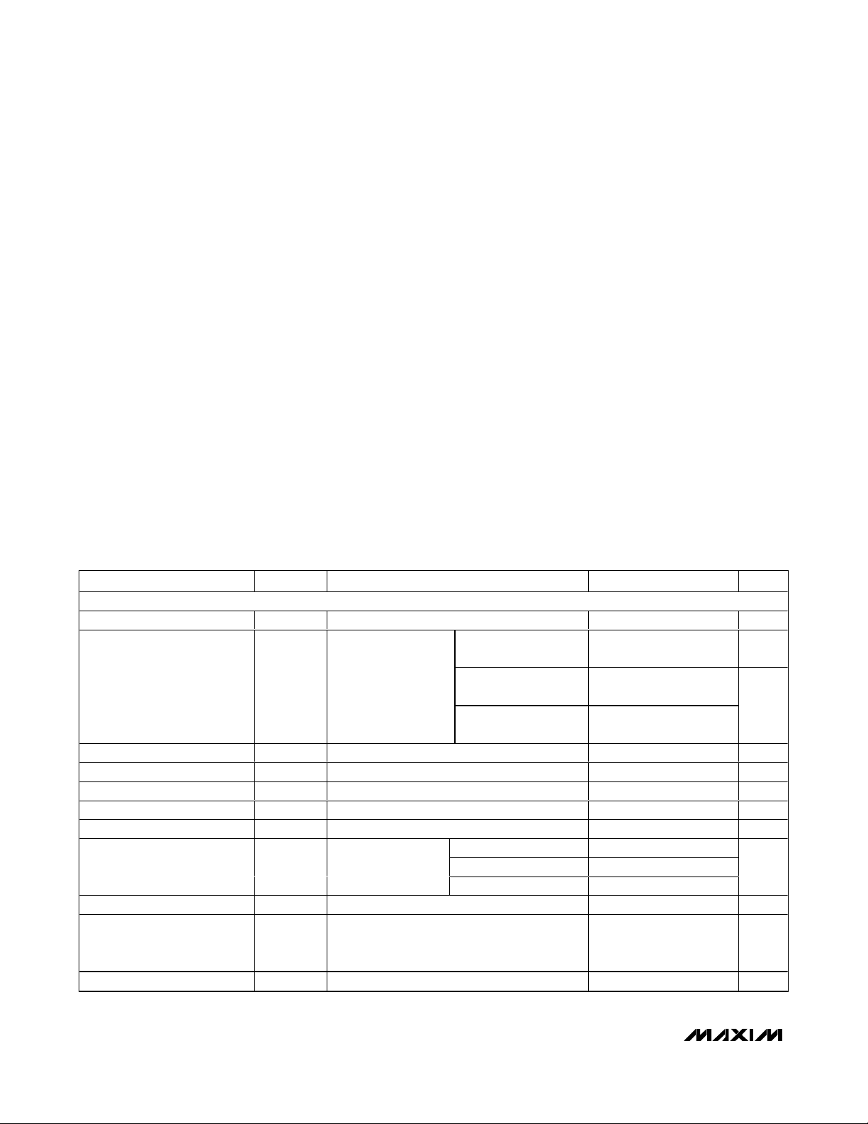
ABSOLUTE MAXIMUM RATINGS
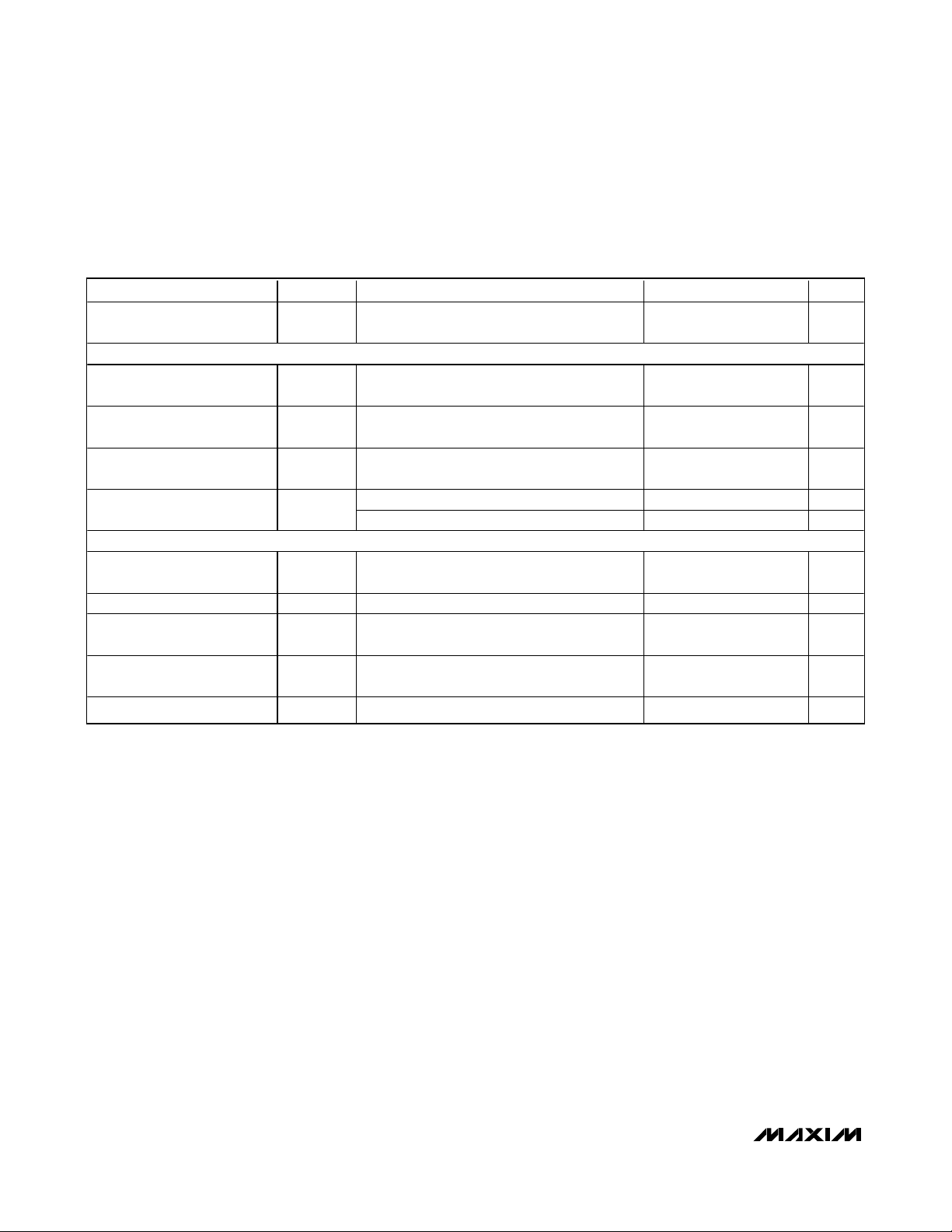
ELECTRICAL CHARACTERISTICS
(Circuit of Figure 1. VDD= VCC= V
SHDN
= V
PSI
= V
DPRSTP
= 5V, DPRSLPVR = GNDS = PGND_ = GND, VFB= V
CCI
= V
CSP
_ = V
CSN
_
= 1.200V, D0–D6 set for 1.20V (D0–D6 = 0001100). T
A
= 0°C to +85°C, unless otherwise specified. Typical values are at TA= +25°C.)
Stresses beyond those listed under “Absolute Maximum Ratings” may cause permanent damage to the device. These are stress ratings only, and functional
operation of the device at these or any other conditions beyond those indicated in the operational sections of the specifications is not implied. Exposure to
absolute maximum rating conditions for extended periods may affect device reliability.
VCC, VDDto GND .....................................................-0.3V to +6V
D0–D6, CSP_ to GND...............................................-0.3V to +6V
CSN12 (MAX8771) to GND ......................................-0.3V to +6V
CSN_ (MAX8770/MAX8772) to GND........................-0.3V to +6V
PHASEGD (MAX8771) to GND.................................-0.3V to +6V
THRM, VRHOT, CLKEN to GND...............................-0.3V to +6V
TIME, PWRGD, POUT to GND......................-0.3V to V
CC
+ 0.3V
REF, FB, CCV, CCI to GND ..........................-0.3V to V
CC
+ 0.3V
SHDN to GND (Note 1)...........................................-0.3V to +14V
TON to GND ...........................................................-0.3V to +30V
DPRSLPVR, DPRSTP, PSI to GND ...........................-0.3V to +6V
GNDS, PGND_ to GND .........................................-0.3V to +0.3V
DL_ to PGND_...............................................-0.3V to V
DD
+ 0.3V
BST_ to GND ..........................................................-0.3V to +36V
LX_ to BST_ ..............................................................-6V to +0.3V
BST_ to VDD...........................................................-0.3V to +30V
DH_ to LX_ ..................................................-0.3V to V
BST_
+0.3V
REF Short Circuit to GND ...........................................Continuous
Continuous Power Dissipation
40-Pin 6mm x 6mm Thin QFN
(derate 23.2mW/°C above +70°C).............................2051mW
Operating Temperature Range .........................-40°C to +105°C
Junction Temperature......................................................+150°C
Storage Temperature Range .............................-65°C to +165°C
Lead Temperature (soldering, 10s) .................................+300°C
Note 1: SHDN may be forced to 12V for the purpose of debugging prototype boards using the no-fault test mode, which disables
fault protection and disables overlapping operation.
)
PARAMETER SYMBOL CONDITIONS MIN TYP MAX UNITS
PWM CONTROLLER
Input Voltage Range VCC, V
DC Output-Voltage Accuracy V
Boot Voltage V
GNDS Input Range V
GNDS Gain A
GNDS Input Bias Current I
FB Input Bias Current I
On-Time Accuracy (Note 3) t
TON Shutdown Input Current SHDN = 0, VIN = 26V, VCC = VDD = 0 or 5V 0.01 0.1 µA
Minimum FB and CCI Voltages
for Pseudo-Fixed-Frequency
Operation
Minimum Off-Time t
BOOT
GNDS
GNDS
GNDS
OFF(MIN
OUT
FB
ON
Includes loadregulation error
(Note 2)
∆V
OUT
CSP_ = CSN_ for both enabled phases -2 +2 µA
VIN = 12V
V
FB
Switching frequency is reduced if FB and/or
CCI are less than this value
(Note 3) 300 375 ns
4.5 5.5 V
-0.4 +0.4 %
-4 +4
-10 +10
1.19 1.20 1.21 V
-200 +200 mV
-25 -15 +2 µA
= V
DD
/∆V
CCI
GNDS,
= 1.2V
DAC codes from
0.8375V to 1.500V
DAC codes from
0.500V to 0.825V
DAC codes below
0.4875V
-200mV ≤ V
R
TON
R
TON
R
TON
≤ +200mV 0.95 1.00 1.05 V/V
GNDS
= 96.75kΩ 142 167 192
= 200kΩ 300 333 366
= 303.25kΩ 425 500 575
0.2 0.25 V
mV
ns
Page 3
MAX8770/MAX8771/MAX8772
MAX8770/MAX8771/MAX8772 Dual-Phase, Quick-
PWM Controller for IMVP-6+ CPU Core Power Supplies
_______________________________________________________________________________________ 3
CONFIDENTIAL INFORMATION – RESTRICTED TO INTEL®IMVP-6 LICENSEES
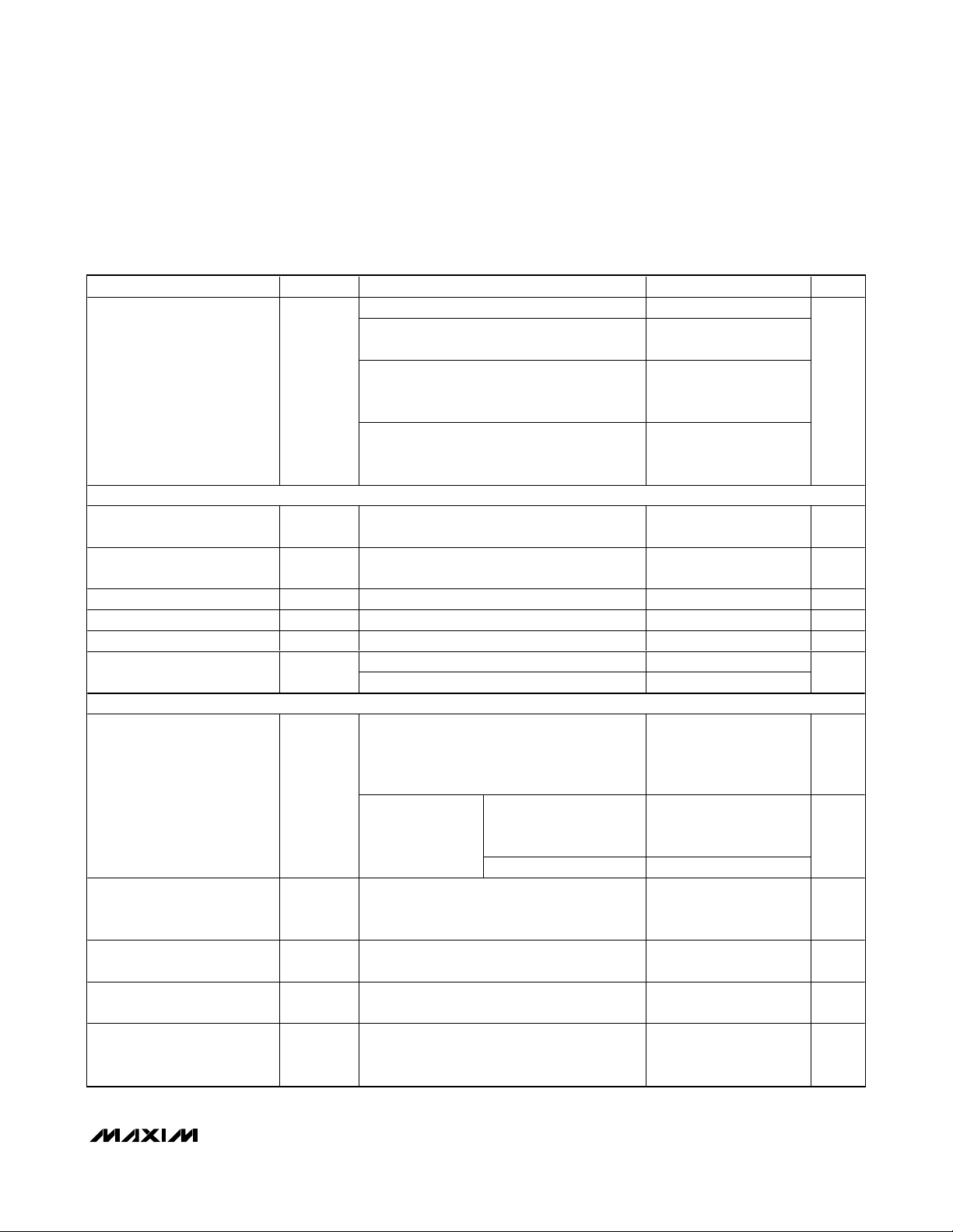
ELECTRICAL CHARACTERISTICS (continued)
(Circuit of Figure 1. VDD= VCC= V
SHDN
= V
PSI
= V
DPRSTP
= 5V, DPRSLPVR = GNDS = PGND_ = GND, VFB= V
CCI
= V
CSP
_ = V
CSN
_
= 1.200V, D0–D6 set for 1.20V (D0–D6 = 0001100). T
A
= 0°C to +85°C, unless otherwise specified. Typical values are at TA= +25°C.)
)
)
PARAMETER SYMBOL CONDITIONS MIN TYP MAX UNITS
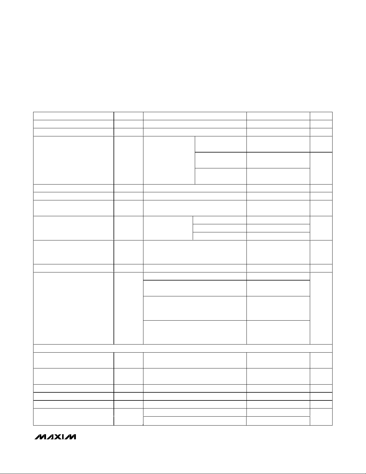
BIAS AND REFERENCE
Qui escent S up p l y C ur r ent ( V
Qui escent S up p l y C ur r ent ( V
S hutd ow n S up p l y C ur r ent ( V
S hutd ow n S up p l y C ur r ent ( V
Reference Voltage V
Reference Load Regulation ∆V
FAULT PROTECTION
Output Overvoltage Protection
Threshold
(MAX8770/MAX8771 Only)
Output OvervoltagePropagation Delay
(MAX8770/MAX8771 Only)
) I
C C
) I
D D
) I
C C
) I
D D
CC
DD
CC(SHDN
DD(SHDN
REF
REF
V
OVP
t
OVP
R
TIME
R
TIME
(5mV/µs nominal)
DPRSTP = high, DPRSLPVR = high,
R
TIME
nominal to 1.25mV/µs nominal
Startup and shutdown, R
(3.125mV/µs nominal) to 178kΩ
(0.625mV/µs nominal)
Measured at VCC, FB forced above the
regulation point, DPRSLPVR = V
Measured at VDD, FB forced above the
regulation point, DPRSLPVR = V
Measured at VCC, SHDN = GND 0.01 1 µA
Measured at VDD, SHDN = GND 0.01 1 µA
V
CC
I
REF
I
REF
Measured at FB with respect to unloaded
output voltage; rising edge;
PWM mode or skip mode after output reaches
the regulation voltage
Measured at FB;
rising edge
FB forced 25mV above trip threshold 10 µs
= 71.5kΩ (12.5mV/µs nominal) -10 +10
= 35.7kΩ (25mV/µs nominal) to 178kΩ
= 35.7kΩ to 178kΩ, SR = 6.25mV/µs
= 4.5V to 5.5V, I
= 0 to 500µA -2 -0.2
= -100µA to 0 0.21 6.2
-15 +15
-20 +20TIME Slew-Rate Accuracy
= 35.7kΩ
TIME
CC
CC
= 0 1.986 2.000 2.014 V
REF
Skip mode and output
have not reached the
regulation voltage
Minimum OVP threshold 0.8
-20 +20
510mA
0.01 1 µA
250 300 350 mV
1.75 1.80 1.85
%
mV
V
Output Undervoltage
Protection Threshold
Output Undervoltage
Propagation Delay
CLKEN Startup Delay
(Boot Time Period)
V
UVP
t
UVP
t
BOOT
Measured at FB with respect to unloaded
output voltage
FB forced 25mV below trip threshold 10 µs
Measured from the time when FB reaches the
boot target voltage based on the slew rate set
by R
TIME
-450 -400 -350 mV
20 60 100 µs
Page 4
MAX8770/MAX8771/MAX8772
MAX8770/MAX8771/MAX8772 Dual-Phase, Quick-
PWM Controller for IMVP-6+ CPU Core Power Supplies
4 _______________________________________________________________________________________
CONFIDENTIAL INFORMATION – RESTRICTED TO INTEL®IMVP-6 LICENSEES
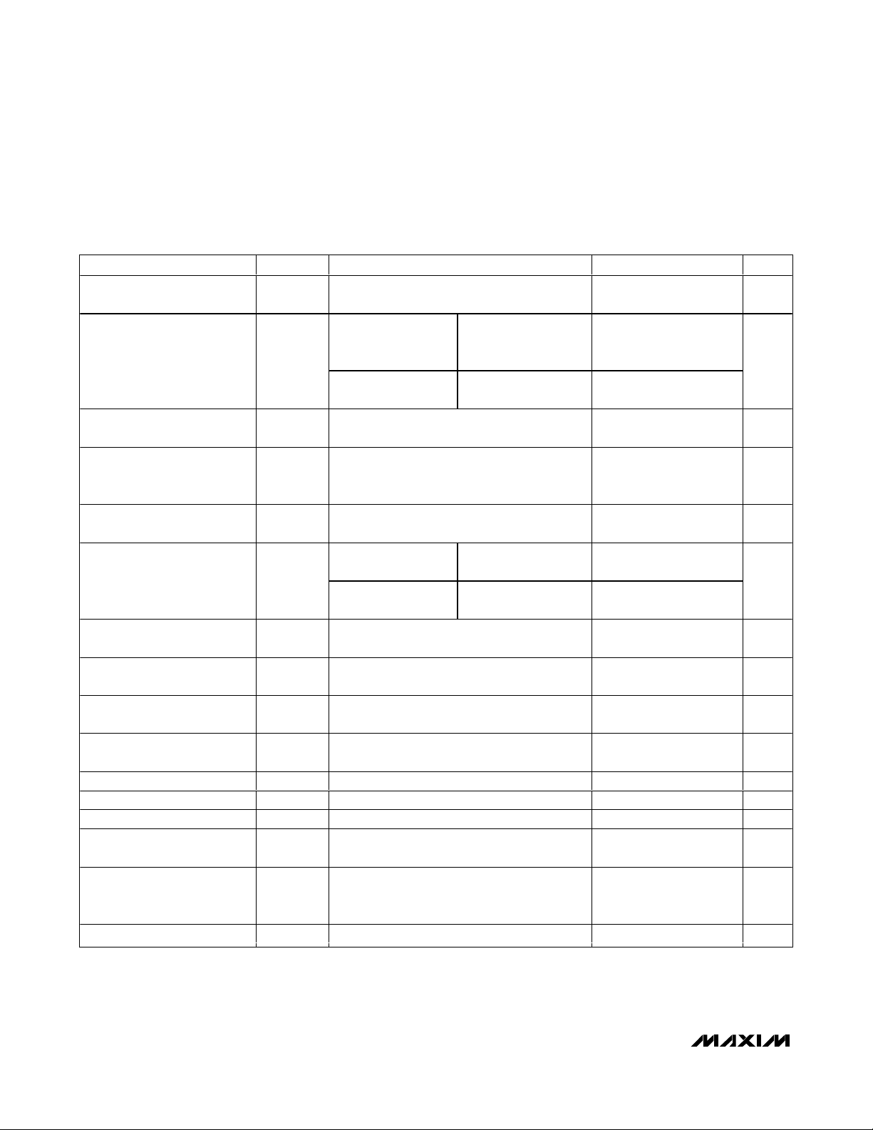
ELECTRICAL CHARACTERISTICS (continued)
(Circuit of Figure 1. VDD= VCC= V
SHDN
= V
PSI
= V
DPRSTP
= 5V, DPRSLPVR = GNDS = PGND_ = GND, VFB= V
CCI
= V
CSP
_ = V
CSN
_
= 1.200V, D0–D6 set for 1.20V (D0–D6 = 0001100). T
A
= 0°C to +85°C, unless otherwise specified. Typical values are at TA= +25°C.)
)
PARAMETER SYMBOL CONDITIONS MIN TYP MAX UNITS
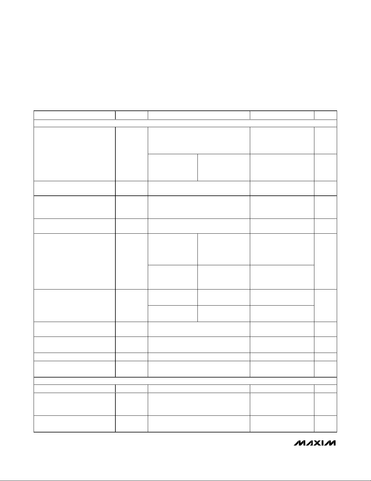
PWRGD, PHASEGD Startup
Delay
CLKEN, PWRGD Threshold
CLKEN, PWRGD, PHASEGD
Delay
t
PWRGD
Measured at startup from the time when
CLKEN goes low
Measured at FB with
respect to unloaded
output voltage
15mV hysteresis (typ)
FB forced 25mV outside the PWRGD trip
thresholds
Lower threshold, falling
edge (undervoltage)
Upper threshold, rising
edge (overvoltage)
mV
358ms
-350 -300 -250
+150 +200 +250
10 µs
CLKEN, PWRGD, PHASEGD
Transition Blanking Time
PHASEGD Transition Blanking
Time
PHASEGD Window
Comparator Thresholds
CLKEN, PWRGD, PHASEGD
Output Low Voltage
CLKEN, PWRGD, PHASEGD
Leakage Current
VRHOT Trip Threshold
VRHOT Delay t
VRHOT Output On-Resistance R
VRHOT Leakage Current High state. VRHOT forced to 5V 1 µA
THRM Input Leakage -100 +100 nA
VCC Undervoltage Lockout
Threshold
VCC Power-On Reset
Threshold
Thermal Shutdown Threshold T
t
BLANK
t
PHASEGD
VRHOT
VRHOT
V
UVLO(VCC
SHDN
Measured from the time when FB reaches the
target voltage based on the slew rate set by
R
TIME
Number of DH2 pulses from when phase 2 is
enabled
V(CCI, FB),
0.4V ≤ V(FB) ≤ 1.5V
15mV hysteresis (typ)
I
= 3mA 0.4 V
SINK
High state, CLKEN, PWRGD, PHASEGD forced
to 5V
Measured at THRM, with respect to V
edge, 115mV hysteresis (typ)
THRM forced 25mV below the VRHOT trip
threshold; falling edge
Low state 3.5 11 Ω
Rising edge, 50mV hysteresis, DL_ pulled low
below this level
Falling edge, typical hysteresis = 1.1V, faults
cleared and DL_ forced high when V
below this level
Hysteresis = 15°C 160 °C
Lower threshold,
0.6V
nominal
FB
Upper threshold,
1.4V
nominal
FB
CC
CC
; falling
falls
-20 +20
-20 +20
29.5 30 30.5 %
4.1 4.25 4.45 V
20 µs
32 Cycles
10 µs
1.8 V
mV
1µA
Page 5
MAX8770/MAX8771/MAX8772
MAX8770/MAX8771/MAX8772 Dual-Phase, Quick-
PWM Controller for IMVP-6+ CPU Core Power Supplies
_______________________________________________________________________________________ 5
CONFIDENTIAL INFORMATION – RESTRICTED TO INTEL®IMVP-6 LICENSEES
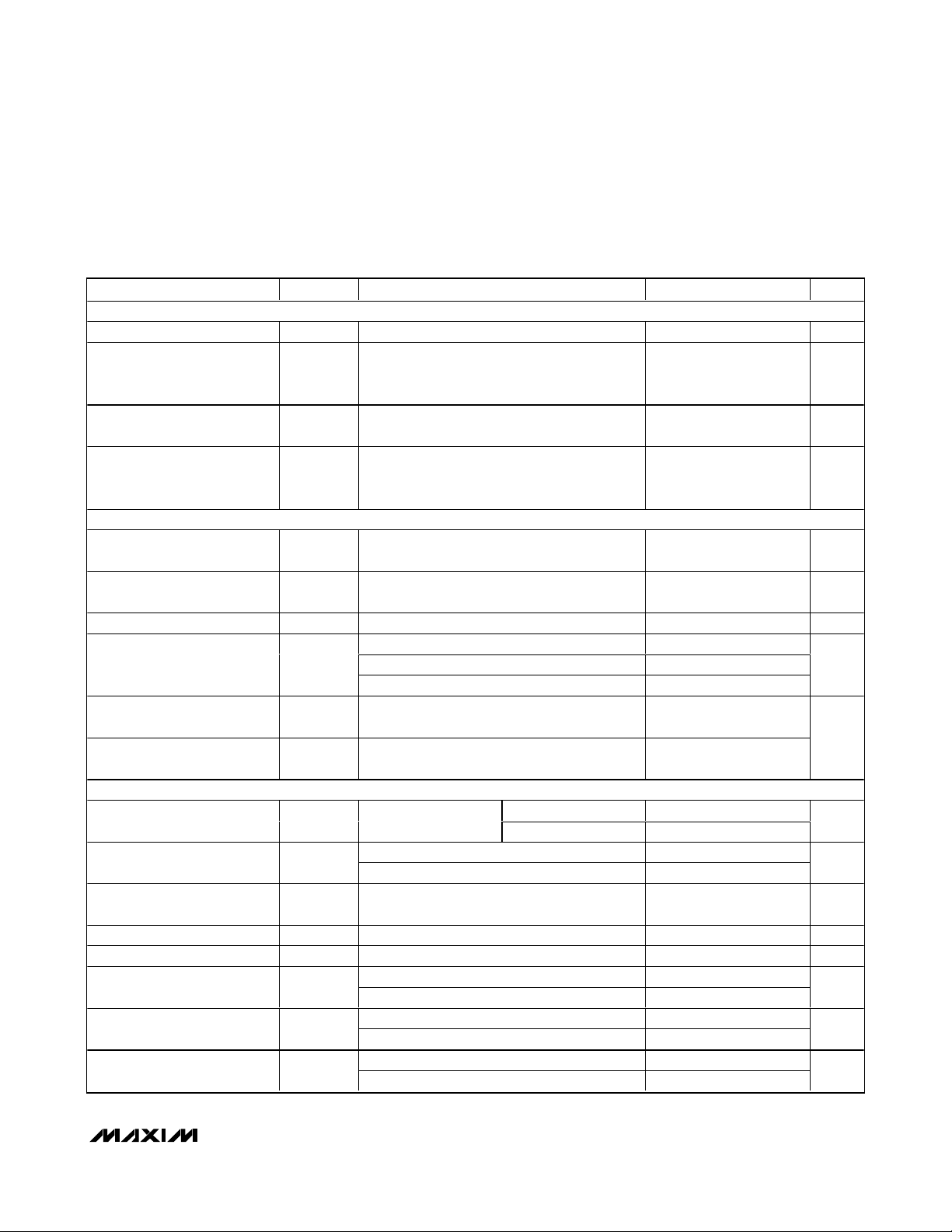
ELECTRICAL CHARACTERISTICS (continued)
(Circuit of Figure 1. VDD= VCC= V
SHDN
= V
PSI
= V
DPRSTP
= 5V, DPRSLPVR = GNDS = PGND_ = GND, VFB= V
CCI
= V
CSP
_ = V
CSN
_
= 1.200V, D0–D6 set for 1.20V (D0–D6 = 0001100). T
A
= 0°C to +85°C, unless otherwise specified. Typical values are at TA= +25°C.)
)
)
)
)
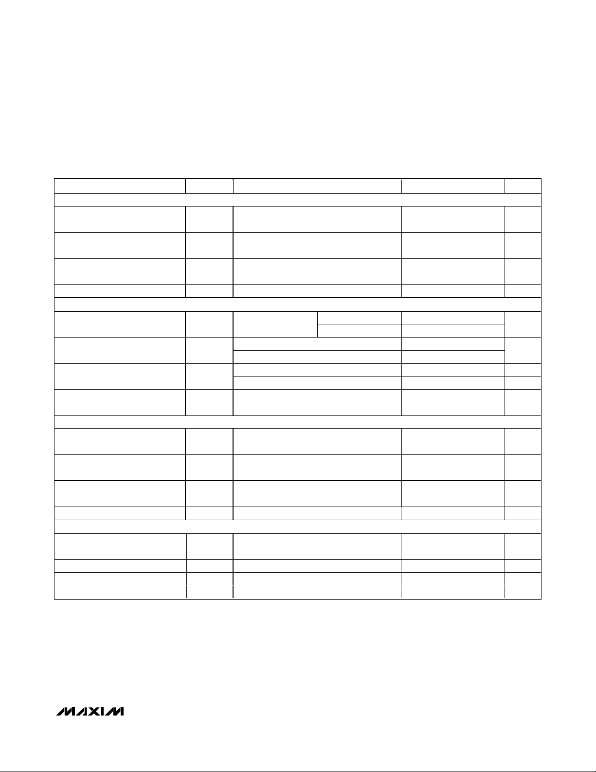
PARAMETER SYMBOL CONDITIONS MIN TYP MAX UNITS
DROOP AND BALANCE
DC Droop Amplifier Offset -1.0 +1.0 mV
DC Droop Amplifier
Transconductance
Current-Balance
Preamplifier Offset
Current-Balance Amplifier
Transconductance
CURRENT LIMIT
Valley Current-Limit Threshold
(Positive)
Valley Current-Limit Threshold
(Negative)
Zero Crossing Threshold V
C om m on- S ense C om m on- M od e
Inp ut Rang e
Phase 2 Disable Threshold
Gate Drivers
GATE DRIVERS
DH_ Gate Driver
On-Resistance
DL_ Gate Driver
On-Resistance
DH_ Gate Driver Source/Sink
Current
D L_ G ate D r i ver S our ce C ur r ent I
DL_ Gate Driver Sink Current I
Driver Propagation Delay
DL_ Transition Time
DH_ Transition Time
G
m(FB)
G
m(CCI
V
LIMIT
ZX
R
ON(DH_
R
ON(DL_
I
DH
D L( S OU RC E )
DL(SINK
∆IFB/(Σ∆VCS),
V
FB
V
CSP
[V(CSP1, CSN_) - V(CSP2, CSN_)] at I
∆ I
CCI
CCI = FB = CSN_ = 0.45V to 1.5V, and
V(CSP_, CSN_) = -10mV to +10mV
CSP_ - CSN_ 19.5 22.5 25.5 mV
CSP_, CSN_ -35 -30 -25 mV
PGND1 - LX1, DPRSLPVR = high (skip mode) 2.5 mV
CSP_ -0.2 +0.2
CSN_ -0.2 +0.2Current-Sense Input Current
CSN12 (MAX8771) -0.4 +0.4
CSP_ -CSN_ 0 2
CSP2 3 V
BST_ -LX_ forced
to 5V
High state (pullup) 0.7 2.0
Low state (pulldown) 0.25 0.5
DH_ forced to 2.5V, BST_ - LX_ forced to 5V 2.2 A
DL_ forced to 2.5V 2.7 A
DL_ forced to 2.5V 8 A
DH_ low to DL_ high 18 25
DL_ low to DH_ high 9 20
DL_ falling, C
DL_ rising, C
DH_ falling, C
DH_ rising, C
= V
_ = 1.2V,
CSN
_ - V
_ = 0 to +60mV
CSN
/∆ [V(CSP1, CSN_), V(CSP2, CSN_)]
High state (pullup) 0.9 2.5
Low state (pulldown) 0.7 2.5
= 3nF 20
DL_
= 3nF 20
DL_
= 3nF 20
DH_
= 3nF 20
DH_
= 0 -1.0 +1.0 mV
CCI
590 600 610 µS
200 µS
- 1 VCC - 0.4
CC
µA
V
Ω
Ω
ns
ns
ns
Page 6
MAX8770/MAX8771/MAX8772
MAX8770/MAX8771/MAX8772 Dual-Phase, Quick-
PWM Controller for IMVP-6+ CPU Core Power Supplies
6 _______________________________________________________________________________________
CONFIDENTIAL INFORMATION – RESTRICTED TO INTEL®IMVP-6 LICENSEES
ELECTRICAL CHARACTERISTICS (continued)
(Circuit of Figure 1. VDD= VCC= V
SHDN
= V
PSI
= V
DPRSTP
= 5V, DPRSLPVR = GNDS = PGND_ = GND, VFB= V
CCI
= V
CSP
_ = V
CSN
_
= 1.200V, D0–D6 set for 1.20V (D0–D6 = 0001100). T
A
= 0°C to +85°C, unless otherwise specified. Typical values are at TA= +25°C.)
PARAMETER SYMBOL CONDITIONS MIN TYP MAX UNITS
Internal Boost Charging Switch
On-Resistance
POWER MONITOR
Power-Monitor Output Voltage
for Typical HFM Conditions
Power-Monitor Gain Referred
to Feedback Voltage
Power-Monitor Gain Referred
to ΣV (CSP_, CSN)
Power-Monitor Load
Regulation
LOGIC AND I/O
Logic Input High Voltage V
SHDN No-Fault Level To enable no-fault mode 11 13 V
Low-Voltage Logic Input High
Voltage
Low-Voltage Logic Input Low
Voltage
Logic Input Current SHDN, PSI, DPRSLPVR, D0–D6 = 0 to 5V -1 +1 µA
V
V
IH
IHLV
ILLV
V
DD
V
FB
Σ∆V
V
FB
Sourcing: I
Sinking: I
SHDN, DPRSLPVR, rising edge,
hysteresis = 200mV
D0–D6, PSI, DRPSTP 0.67 V
D0–D6, PSI, DRPSTP 0.33 V
to BST_ 10 20 Ω
- V
CS
- V
= 1.200V, Σ∆VCS = 30mV 2.08 2.16 2.24 V
GNDS
= 30mV 1.72 1.80 1.88 V/V
= 1.200V, TA = +25°C to +85°C 70.5 72 73.5 V/V
GNDS
= 0 to 500µA -6 µV/µA
POUT
= 0 to 100µA 50 mV
POUT
1.2 1.7 2.3 V
Page 7
MAX8770/MAX8771/MAX8772
MAX8770/MAX8771/MAX8772 Dual-Phase, Quick-
PWM Controller for IMVP-6+ CPU Core Power Supplies
_______________________________________________________________________________________ 7
CONFIDENTIAL INFORMATION – RESTRICTED TO INTEL®IMVP-6 LICENSEES
ELECTRICAL CHARACTERISTICS
(Circuit of Figure 1. VDD= VCC= V
SHDN
= V
PSI
= V
DPRSTP
= 5V, DPRSLPVR = GNDS = PGND_ = GND, VFB= V
CCI
= V
CSP
_ = V
CSN
_
= 1.200V, D0–D6 set for 1.20V (D0-D6 = 0001100). T
A
= -40°C to +105°C, unless otherwise specified. Typical values are at TA=
+25°C.) (Note 4)
)
)
)
PARAMETER SYMBOL CONDITIONS MIN TYP MAX UNITS
PWM CONTROLLER
Input Voltage Range VCC, V
DC Output Voltage Accuracy V
Boot Voltage V
GNDS Input Range V
GNDS Gain A
Minimum FB and CCI Voltages
for Pseudo-Fixed-Frequency
Operation
Minimum Off-Time t
OUT
BOOT
GNDS
GNDS
ON
OFF(MIN
Includes loadregulation error
(Note 2)
∆V
+200mV
VIN = 12V
V
FB
Switching frequency is reduced if FB and/or
CCI are less than this value
(Note 3) 375 ns
R
TIME
R
TIME
178kΩ (5mV/µs nominal)
DD
DAC codes from
0.8375V to 1.500V
DAC codes from
0.500V to 0.825V
DAC codes below
0.4875V
4.5 5.5 V
-0.6 +0.6 %
-6 +6
-15 +15
1.182 1.218 V
-200 +200 mV
OUT
= V
/∆V
CCI
GNDS,
= 1.2V
-200mV ≤ V
R
TON
R
TON
R
TON
≤
GNDS
0.95 1.05 V/V
= 96.75kΩ 142 192
= 200kΩ 300 366On-Time Accuracy (Note 3) t
= 303.25kΩ 425 575
0.25 V
= 71.5kΩ (12.5mV/µs nominal) -10 +10
= 35.7kΩ (25mV/µs nominal) to
-15 +15
mV
ns
TIME Slew-Rate Accuracy
BIAS AND REFERENCE
Quiescent Supply Current (VCC)I
Quiescent Supply Current (VDD)I
Shutdown Supply Current (VCC)I
Shutdown Supply Current (VDD)I
Reference Voltage V
Reference Load Regulation ∆V
CC
DD
CC(SHDN
DD(SHDN
REF
REF
DPRSTP = high, DPRSLPVR = high, R
= 35.7kΩ to 178kΩ, SR = 6.25mV/µs
TIME
-20 +20
%
nominal to 1.25mV/µs nominal
Startup and shutdown,
R
= 35.7kΩ (3.125mV/µs nominal) to
TIME
-20 +20
178kΩ (0.625mV/µs nominal)
Measured at VCC, FB forced above the
regulation point, DPRSLPVR = V
CC
Measured at VDD, FB forced above the
regulation point, DPRSLPVR = V
CC
10 mA
1µA
Measured at VCC, SHDN = GND 1 µA
Measured at VDD, SHDN = GND 1 µA
V
= 4.5V to 5.5V, I
CC
I
= 0 to 500µA -2
REF
I
= -100µA to 0 6.2
REF
= 0 1.98 2.02 V
REF
mV
Page 8
MAX8770/MAX8771/MAX8772
MAX8770/MAX8771/MAX8772 Dual-Phase, Quick-
PWM Controller for IMVP-6+ CPU Core Power Supplies
8 _______________________________________________________________________________________
CONFIDENTIAL INFORMATION – RESTRICTED TO INTEL®IMVP-6 LICENSEES
ELECTRICAL CHARACTERISTICS (continued)
(Circuit of Figure 1. VDD= VCC= V
SHDN
= V
PSI
= V
DPRSTP
= 5V, DPRSLPVR = GNDS = PGND_ = GND, VFB= V
CCI
= V
CSP
_ = V
CSN
_ =
1.200V, D0–D6 set for 1.20V (D0-D6 = 0001100). T
A
= -40°C to +105°C, unless otherwise specified. Typical values are at TA= +25°C.)
(Note 4)
)
PARAMETER SYMBOL CONDITIONS MIN TYP MAX UNITS
FAULT PROTECTION
Output Overvoltage Protection
Threshold
(MAX8770/MAX8771 Only)
Output Undervoltage Protection
Threshold
CLKEN Startup Delay (Boot Time
Period)
PWRGD, PHASEGD Startup
Delay
CLKEN, PWRGD Threshold
V
OVP
V
UVP
t
BOOT
t
PWRGD
Measured at FB with respect to unloaded
output voltage, rising edge,
PWM mode, or skip mode after output
reaches the regulation voltage
Skip mode and
Measured at FB,
rising edge
Measured at FB with respect to unloaded
output voltage
Measured from the time when FB reaches
the boot target voltage based on the slew
rate set by R
Measured at startup from the time when
CLKEN goes low
Measured at FB
with respect to
unloaded output
voltage
15mV hysteresis
(typ)
TIME
output have not
reached the
regulation voltage
Lower threshold,
falling edge
(undervoltage)
Upper threshold,
rising edge
(overvoltage)
250 350 mV
1.75 1.85 V
-450 -350 mV
20 100 µs
38ms
-350 -250
+150 +250
mV
V(CCI,FB),
PHASEGD Window Comparator
Thresholds
CLKEN, PWRGD, PHASEGD
Output Low Voltage
VRHOT Trip Threshold V
VRHOT Output On-Resistance R
VCC Undervoltage Lockout
Threshold
DROOP AND BALANCE
DC Droop Amplifier Offset -1.5 +1.5 mV
DC Droop Amplifier
Transconductance
Current-Balance
Preamplifier Offsets
HOT
VRHOT
V
UVLO(VCC
G
m(FB)
0.4V ≤ V(FB) ≤ 1.5V
15mV hysteresis
(typ)
= 3mA 0.4 V
I
SINK
Measured at THRM, with respect to VCC,
falling edge, 115mV hysteresis (typ)
Low state 11 Ω
Rising edge, 50mV hysteresis, DL_ pulled
low below this level
∆IFB/(Σ∆VCS),
V
= V
FB
V
CSP
[V(CSPI, CSN_) - V(CPS2, CSN_)]
at I
CCI
_ - V
= 0
_ = 1.2V,
CSN
_ = 0 to +60mV
CSN
Lower threshold,
nominal
0.6V
FB
Upper threshold,
nominal
1.4V
FB
-20 +20
-20 +20
29.5 30.5 %
4.1 4.45 V
580 620 µs
-1.5 +1.5 mV
mV
Page 9
MAX8770/MAX8771/MAX8772
MAX8770/MAX8771/MAX8772 Dual-Phase, Quick-
PWM Controller for IMVP-6+ CPU Core Power Supplies
_______________________________________________________________________________________ 9
CONFIDENTIAL INFORMATION – RESTRICTED TO INTEL®IMVP-6 LICENSEES
ELECTRICAL CHARACTERISTICS (continued)
(Circuit of Figure 1. VDD= VCC= V
SHDN
= V
PSI
= V
DPRSTP
= 5V, DPRSLPVR = GNDS = PGND_ = GND, VFB= V
CCI
= V
CSP
_ = V
CSN
_ =
1.200V, D0–D6 set for 1.20V (D0-D6 = 0001100). T
A
= -40°C to +105°C, unless otherwise specified. Typical values are at TA= +25°C.)
(Note 4)
)
)
Note 2: DC output accuracy specifications refer to the trip level of the error amplifier. The output voltage has a DC regulation higher
than the trip level by 50% of the output ripple. When pulse skipping, the output rises by approximately 1.5% when transitioning from continuous conduction to no load.
Note 3: On-time and minimum off-time specifications are measured from 50% to 50% at the DH_ and DH_ pins, with LX_ forced to
GND, BST_ forced to 5V, and a 500pF capacitor from DH_ to LX_ to simulate external MOSFET gate capacitance. Actual incircuit times may be different due to MOSFET switching speeds.
Note 4: Specifications to T
A
= -40°C and +105°C are guaranteed by design and are not production tested.
PARAMETER SYMBOL CONDITIONS MIN TYP MAX UNITS
CURRENT LIMIT
Valley Current-Limit Threshold
(Positive)
Valley Current-Limit Threshold
(Negative)
Current-Sense Common-Mode
Input Range
Phase 2 Disable Threshold CSP2 3 VCC - 0.4 V
GATE DRIVERS
DH_ Gate Driver On-Resistance R
DL_ Gate Driver On-Resistance R
Driver Propagation Delay
Internal Boost Charging Switch
On-Resistance
POWER MONITOR
Power-Monitor Output Voltage for
Typical HFM Conditions
Power-Monitor Gain Referred to
Feedback Voltage
Power-Monitor Gain Referred to
ΣV(CSP_,CSN)
Power-Monitor Load Regulation Sourcing: I
LOGIC AND I/O
Logic-Input High Voltage V
Low-Voltage Logic-Input High
Low-Voltage Logic-Input Low
V
LIMIT
ON(DH_
ON(DL_
IH
V
IHLV
V
ILLV
CSP_ - CSN_ 18.5 26.5 mV
CSP_ - CSN_ -36 -24 mV
CSP_, CSN_ 0 2 V
BST_ – LX_ forced
to 5V
High state (pullup) 2.0
Low state (pulldown) 0.5
DH_ Low to DL_ High 15 ns
DL_ Low to DH_ High 9
V
to BST_ 20 Ω
DD
V
- V
FB
Σ∆V
CS
V
- V
FB
SHDN, DPRSLPVR, rising edge,
hysteresis = 200mV
D0–D6, PSI, DRPSTP 0.67 V
D0–D6, PSI, DRPSTP 0.33 V
= 1.200V, Σ∆VCS = 30mV 2.04 2.28 V
GNDS
= 30mV 1.70 1.90 V/V
= 1.200V 70 74 V/V
GNDS
POUT
High state (pullup) 2.5
Low state (pulldown) 2.5
= 0 to 500µA -6 µV/µA
1.2 2.3 V
Ω
Ω
Page 10
MAX8770/MAX8771/MAX8772
MAX8770/MAX8771/MAX8772 Dual-Phase, Quick-
PWM Controller for IMVP-6+ CPU Core Power Supplies
10 ______________________________________________________________________________________
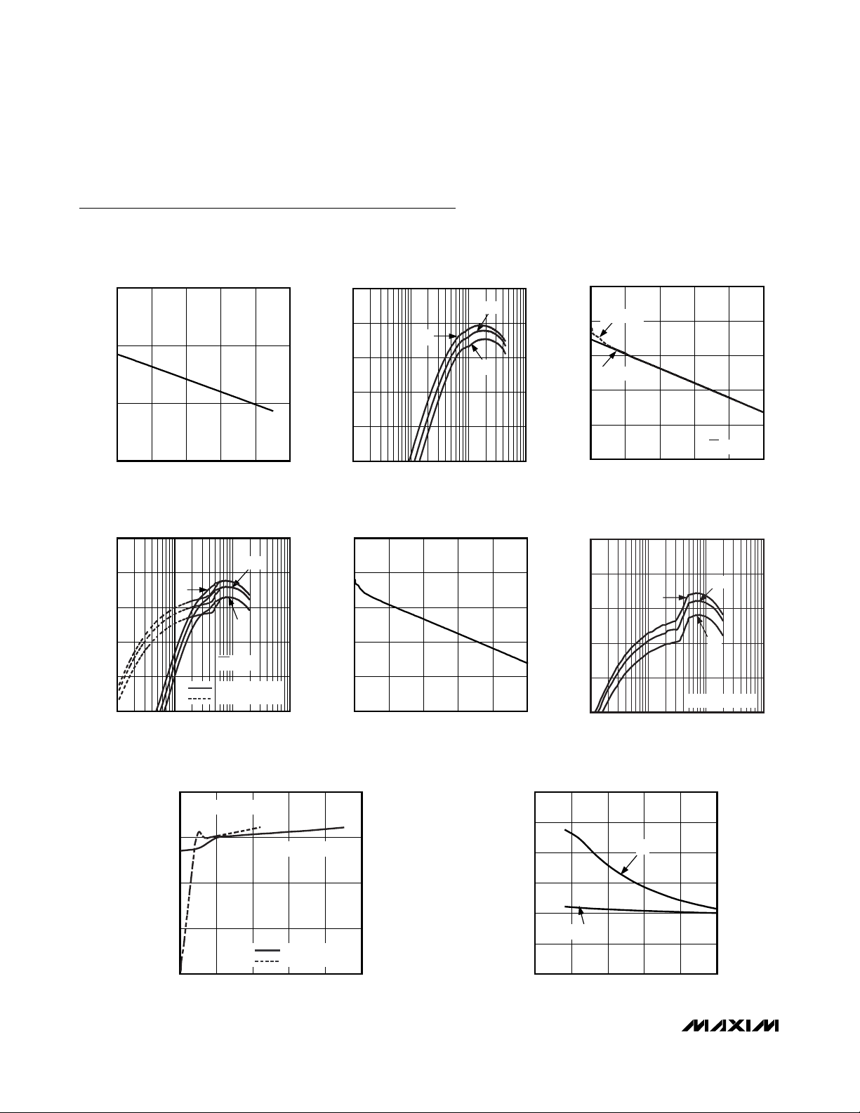
Typical Operating Characteristics
(Circuit of Figure 1. VIN= 12V, VCC= VDD, SHDN = PSI = 5V, DPRSLPVR = GND, D0–D6 set for 1.1500V, TA= 25°C, unless otherwise specified.)
OUTPUT VOLTAGE vs. LOAD CURRENT
(V
OUT(HFM)
= 1.2875V)
LOAD CURRENT (A)
OUTPUT VOLTAGE (V)
MAX8770 toc01
0 1020304050
1.1
1.2
1.3
1.4
EFFICIENCY vs. LOAD CURRENT
(V
OUT(HFM)
= 1.2875V)
LOAD CURRENT (A)
EFFICIENCY (%)
MAX8770 toc02
50
60
70
80
90
100
0.1 1 10 100
12V
7V
20V
OUTPUT VOLTAGE vs. LOAD CURRENT
(V
OUT(LFM)
= 0.9500V)
LOAD CURRENT (A)
OUTPUT VOLTAGE (V)
MAX8770 toc03
0 4 8 12 16 20
0.88
0.90
0.92
0.94
0.96
0.98
PWM MODE
SKIP MODE
PSI = GND
EFFICIENCY vs. LOAD CURRENT
(V
OUT(LFM)
= 0.9500V)
LOAD CURRENT (A)
EFFICIENCY (%)
MAX8770 toc04
50
60
70
80
90
100
0.1 1 10 100
12V
7V
20V
DPRSLPVR = GND
DPRSLPVR = V
CC
PSI - GND
OUTPUT VOLTAGE
vs. LOAD CURRENT (V
OUT(C4)
= 0.6500V)
LOAD CURRENT (A)
OUTPUT VOLTAGE (V)
MAX8770 toc05
0 4 8 12 16 20
0.58
0.60
0.62
0.64
0.66
0.68
CONFIDENTIAL INFORMATION – RESTRICTED TO INTEL®IMVP-6 LICENSEES
SWITCHING FREQUENCY
vs. LOAD CURRENT
LOAD CURRENT (A)
SWITCHING FREQUENCY (kHz)
MAX8770 toc07
0 1020304050
0
100
200
300
400
V
OUT(HFM)
= 1.2875V
V
OUT(LFM)
= 0.9500V
DPRSLPVR = GND
DPRSLPVR = V
CC
NO-LOAD SUPPLY CURRENT
vs. INPUT VOLTAGE (V
OUT(HFM)
= 1.2875V)
INPUT VOLTAGE (V)
SUPPLY CURRENT (mA)
MAX8770 toc08
0 5 10 15 20 25
0
25
50
75
100
125
150
I
IN
ICC + I
DD
EFFICIENCY vs. LOAD CURRENT
= 0.6500V)
(V
100
90
80
70
EFFICIENCY (%)
60
50
0.1 1 10 100
OUT(C4)
7V
DPRSLPVR = V
LOAD CURRENT (A)
20V
12V
MAX8770 toc06
CC
Page 11
MAX8770/MAX8771/MAX8772
MAX8770/MAX8771/MAX8772 Dual-Phase, Quick-
PWM Controller for IMVP-6+ CPU Core Power Supplies
______________________________________________________________________________________ 11
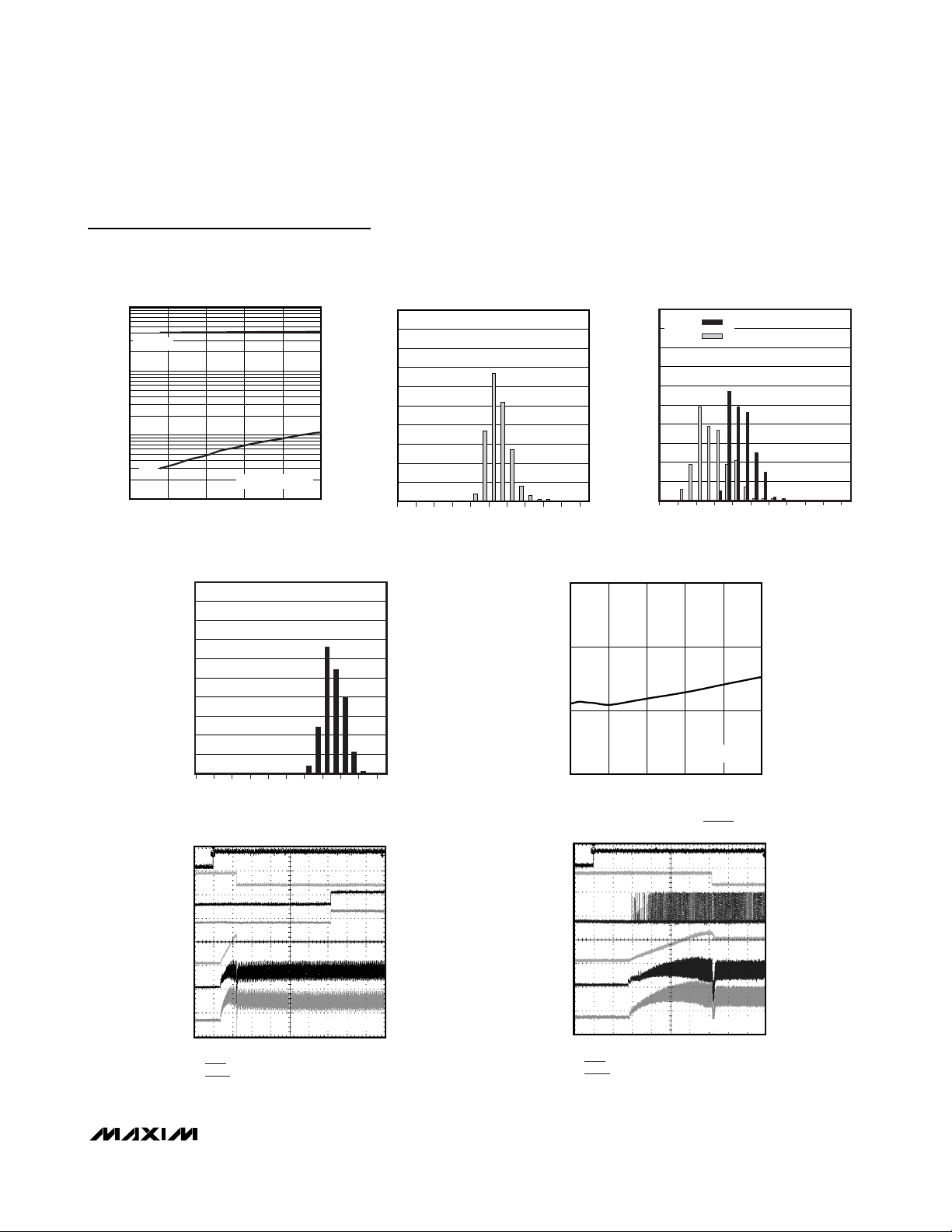
Typical Operating Characteristics (continued)
(Circuit of Figure 1. VIN= 12V, VCC= VDD, SHDN = PSI = 5V, DPRSLPVR = GND, D0–D6 set for 1.1500V, TA= 25°C, unless otherwise specified.)
CONFIDENTIAL INFORMATION – RESTRICTED TO INTEL®IMVP-6 LICENSEES
SOFT-START (UP TO PWRGD)
1ms/div
MAX8770 toc14
0
0
0
0
0
0
0
A
B
C
D
E
F
G
A. SHDN, 5V/div
B. CLKEN, 10V/div
C. PWRGD, 10V/div
D. PHASEGD, 10V/div
E. V
OUT
, 1V/div
F. I
LXI
, 10A/div
G. I
LX2
, 10V/div
R
LOAD
= 65mΩ
SOFT-START (UP TO CLKEN)
200µs/div
MAX8770 toc15
0
0
0
0
0
0
A
B
C
D
E
F
A. SHDN, 5V/div
B. CLKEN, 10V/div
C. LX1, 10V/div
D. V
OUT
, 1V/div
E. I
LXI
, 10A/div
F. I
LX2
, 10V/div
R
LOAD
= 65mΩ
10
0.1
SUPPLY CURRENT (mA)
0.01
NO-LOAD SUPPLY CURRENT
vs. INPUT VOLTAGE AT SKIP MODE
ICC + I
DD
1
I
IN
0 5 10 15 20 25
INPUT VOLTAGE (V)
DPRSLPVR = V
G
TRANSCONDUCTANCE
m(FB)
DISTRIBUTION
100
SAMPLE SIZE = 200
80
60
40
SAMPLE PERCENTAGE (%)
20
0
595 597 599 601 603 605
TRANSCONDUCTANCE (µS)
REFERENCE VOLTAGE DISTRIBUTION
100
MAX8770 toc09
CC
80
60
40
SAMPLE PERCENTAGE (%)
20
0
1.990 2.000 2.010
REFERENCE VOLTAGE (V)
SAMPLE SIZE = 200
MAX8770 toc10
OUTPUT OFFSET VOLTAGE DISTRIBUTION
100
1.2000V
0.8125V
80
60
40
SAMPLE PERCENTAGE (%)
20
0
-3 -2 -1 1 2 3
OUTPUT OFFSET VOLTAGE (mV)
SAMPLE SIZE = 200
INDUCTOR CURRENT DIFFERENCE
vs. LOAD CURRENT
0.3
MAX8770 toc12
0.2
(A)
L(CM)
- I
L(CS)
I
0.1
0
0 5 10 15 20 25
INPUT VOLTAGE (V)
R
SENSE
= 1mΩ
MAX8770 toc13
MAX8770 toc11
Page 12
MAX8770/MAX8771/MAX8772
MAX8770/MAX8771/MAX8772 Dual-Phase, Quick-
PWM Controller for IMVP-6+ CPU Core Power Supplies
12 ______________________________________________________________________________________
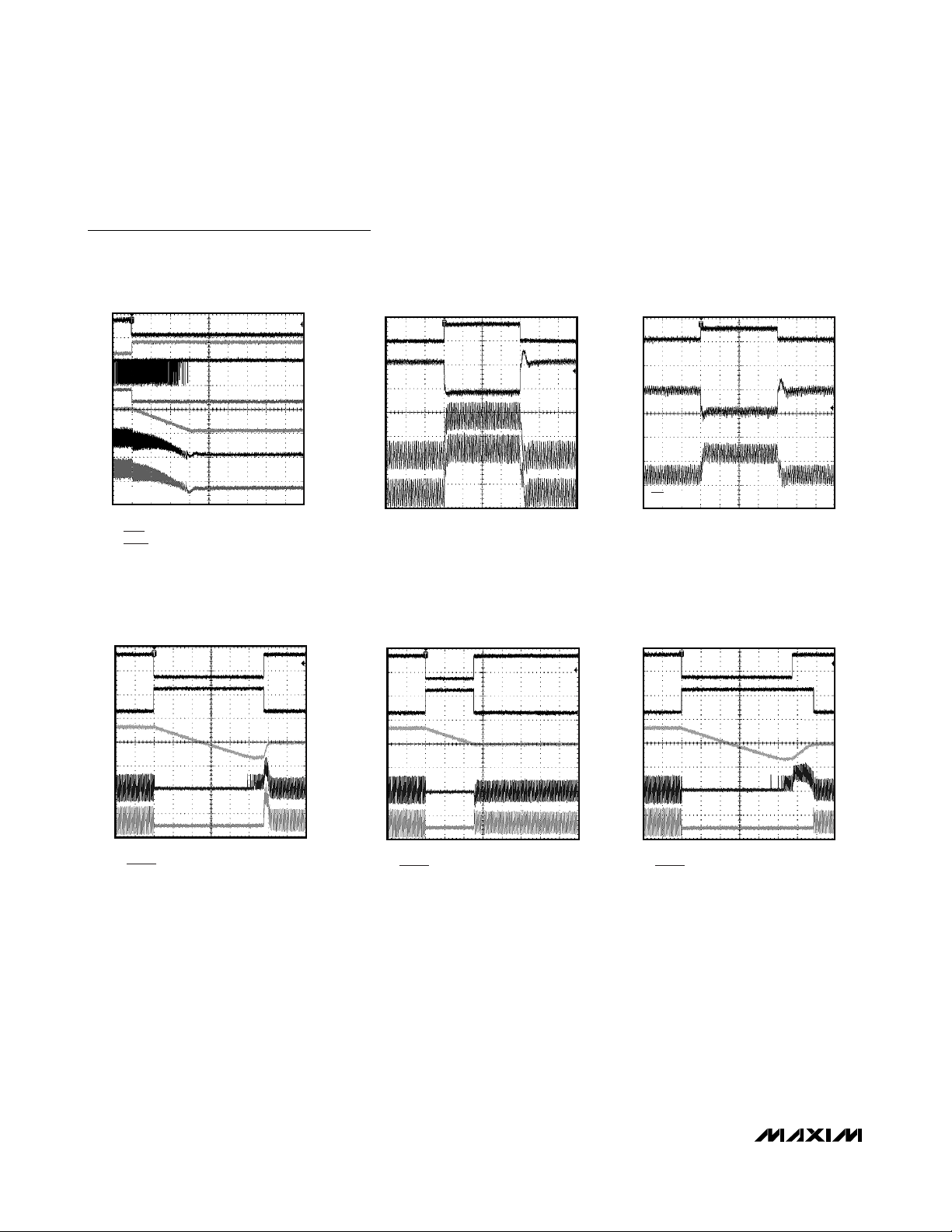
Typical Operating Characteristics (continued)
(Circuit of Figure 1. VIN= 12V, VCC= VDD, SHDN = PSI = 5V, DPRSLPVR = GND, D0–D6 set for 1.1500V, TA= 25°C, unless otherwise specified.)
SHUTDOWN WAVEFORMS
200µs/div
MAX8770 toc16
0
0
0
0
0
0
A
B
C
D
E
F
G
A. SHDN, 5V/div
B. CLKEN, 10V/div
C. DL1, 10V/div
D. PWRGD, 10V/div
E. V
OUT
, 1V/div
F. I
LXI
, 10A/div
G. I
LX2
, 10V/div
R
LOAD
= 65mΩ
HFM LOAD TRANSIENT
(V
OUT(HFM)
= 1.2875V
40µs/div
MAX8770 toc17
0
1.28V
1.22V
20A
0
0
A
B
C
D
A. I
OUT
= 5A TO 36A, 10A/div
B. V
OUT
, 50mV/div
C. I
LXI
, 10A/div
D. I
LX2
,10A/div
ENTERING DEEPER SLEEP
EXITING TO LFM
100µs/div
MAX8770 toc19
0
0
1.28V
0
0
A
B
D
C
E
A. DPRSTP, 5V/div
B. DPRSLPVR, 5V/div
C. V
OUT
, 500mV/div
I
OUT
= 2A
D. I
LXI
, 10A/div
E. I
LX2
, 10A/div
ENTERING DEEPER SLEEP
EXITING TO NEAREST VID
100µs/div
MAX8770 toc20
0
0
0
0
A
B
D
C
E
A. DPRSTP, 5V/div
B. DPRSLPVR, 5V/div
C. V
OUT
, 500mV/div
I
OUT
= 2A
D. I
LXI
, 10A/div
E. I
LX2
, 10A/div
LFM LOAD TRANSIENT
(V
OUT(LFM)
= 0.9500V
40µs/div
MAX8770 toc18
0
0.94V
0.92V
10A
0
A
B
C
A. I
OUT
= 5A TO 15A, 10A/div
B. V
OUT
, 50mV/div
C. I
LXI
, 10A/div
D. I
LX2
,10A/div
PSI = 0
ENTERING DEEPER SLEEP
EXITING TO LFM
100µs/div
MAX8770 toc21
0
0
1.28V
0
0
A
B
D
C
E
A. DPRSTP, 5V/div
B. DPRSLPVR, 5V/div
C. V
OUT
, 500mV/div
I
OUT
= 2A
D. I
LXI
, 10A/div
E. I
LX2
, 10A/div
CONFIDENTIAL INFORMATION – RESTRICTED TO INTEL®IMVP-6 LICENSEES
Page 13
MAX8770/MAX8771/MAX8772
MAX8770/MAX8771/MAX8772 Dual-Phase, Quick-
PWM Controller for IMVP-6+ CPU Core Power Supplies
______________________________________________________________________________________ 13
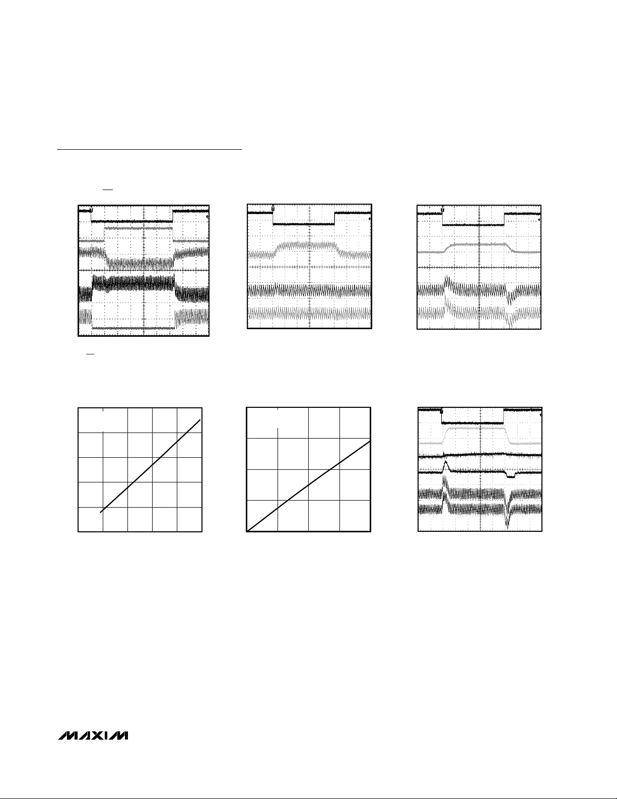
Typical Operating Characteristics (continued)
(Circuit of Figure 1. VIN= 12V, VCC= VDD, SHDN = PSI = 5V, DPRSLPVR = GND, D0–D6 set for 1.1500V, TA= 25°C, unless otherwise specified.)
CONFIDENTIAL INFORMATION – RESTRICTED TO INTEL®IMVP-6 LICENSEES
PSI + 1-LSB TRANSITION
40µs/div
MAX8770 toc22
0
0
0.93V
0
0
A
B
D
C
E
A. PSI, 5V/div
B. D0, 5V/div
C. V
OUT
, 20mV/div
I
OUT
= 10A
D. I
LXI
, 10A/div
E. I
LX2
, 10A/div
D0 DYNAMIC VID CODE CHANGE
20µs/div
MAX8770 toc23
0
0.93V
0
0
A
B
D
C
A. D0, 5V/div
B. V
OUT
, 20mV/div
I
OUT
= 10A
C. I
LXI
, 10A/div
D. I
LX2
, 10A/div
POWER MONITOR vs. OUTPUT VOLTAGE
OUTPUT VOLTAGE (V)
POWER MONITOR (V) .
MAX8770 toc25
0 0.3 0.6 0.9 1.2 1.5
0
0.2
0.4
0.6
0.8
1.0
R
SENSE
= 1mΩ
I
OUT
= 10A
POWER MONITOR vs. LOAD CURRENT
LOAD CURRENT (A)
POWER MONITOR (V) .
MAX8770 toc26
0 10203040
0
1
2
3
4
R
SENSE
= 1mΩ
V
OUT
= 1.2875V
D3 DYNAMIC VID CODE CHANGE
20µs/div
MAX8770 toc24
0
0.93V
0
0
A
B
C
D
A. D3, 5V/div
B. V
OUT
, 200mV/div
I
OUT
= 10A
C. I
LXI
, 10A/div
D. I
LX2
, 10A/div
0
0
0.72V
0
1.185
0A
B
C
D
E
F
POWER MONITOR -
VID TRANSITION RESPONSE
MAX8770 TOC28
40µs/div
A. D3, 5V/div
B. V
OUT
, 200mV/div
C. POUT WITH RC FILTER
(10kΩ, 0.1µF), 200mV/div
D. POUT, 2V/div
E. I
LX1
, 10A/div
F. I
LX2
, 10A/div
I
OUT
= 10A
Page 14
MAX8770/MAX8771/MAX8772
MAX8770/MAX8771/MAX8772 Dual-Phase, Quick-
PWM Controller for IMVP-6+ CPU Core Power Supplies
14 ______________________________________________________________________________________
CONFIDENTIAL INFORMATION – RESTRICTED TO INTEL®IMVP-6 LICENSEES
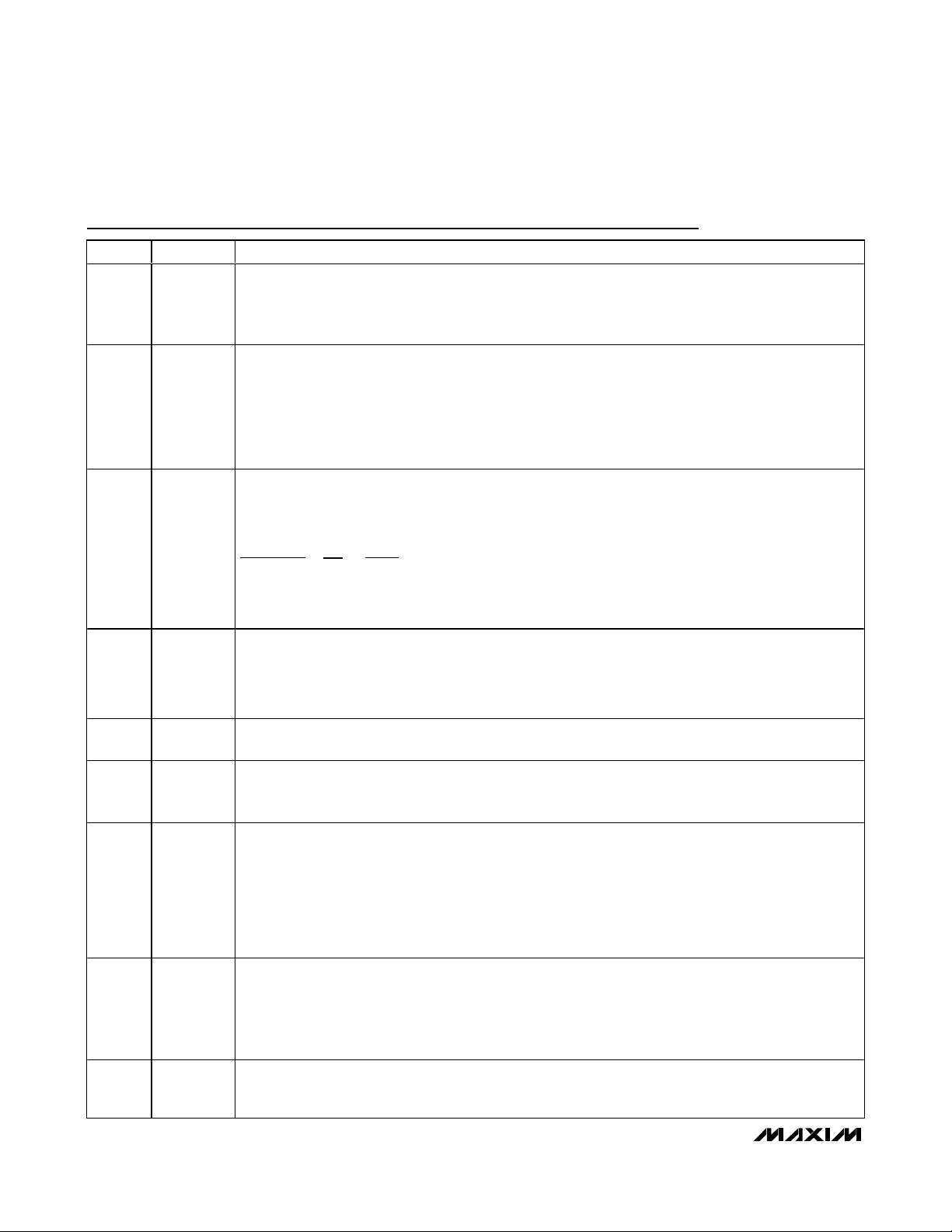
Pin Description
PIN NAME FUNCTION
Clock-Enable Logic Output. This inverted logic output indicates when the output voltage sensed at FB is in
1 CLKEN
2 PWRGD
3 PSI
4 POUT
5 VRHOT
6 THRM
regulation. CLKEN is forced low during VID transitions. Except during startup, CLKEN is the inverse of
PWRGD. See the Startup Timing Diagram (Figure 9). When in pulse-skipping mode (DPRSLPVR high), the
upper CLKEN threshold is disabled.
Open-Drain, Power-Good Output. After output-voltage transitions, except during power-up and power-
down, if FB is in regulation then PWRGD is high impedance. During startup, PWRGD is held low and
continues to be low while the part is in boot mode and until 5ms (typ) after CLKEN goes low.
PWRGD is forced low in shutdown. PWRGD is forced high impedance whenever the slew-rate controller is
active (output-voltage transitions).
When in pulse-skipping mode (DPRSLPVR high), the upper PWRGD threshold comparator is blanked.
A pullup resistor on PWRGD causes additional finite shutdown current.
Logic Input to Indicate Power Usage. PSI and DPRSLPVR together determine the operating mode as
shown in the truth table below. Blank the PWRGD upper threshold when the part is in skip mode. The part
is forced into full-phase PWM mode during startup, while in boot mode, during the transition from
boot mode to VID mode and during shutdown:
DPRSLPVR PSI Mode
1 0 Very low current (1-phase skip)
1 1 Low current (approximately 3A) (1-phase skip)
0 0 Intermediate power potential (1-phase PWM)
0 1 Max power potential (2- or 1-phase PWM as configured at CSP2)
Power-Monitor Output: V
monitor scale factor:
CSNpm = CSN12 for MAX8771.
CSNpm = CSN2 for MAX8770/MAX8772.
POUT is zero in shutdown.
POUT
= K
x V(CSNpm, GNDS) x ΣV(CSP_, CSN_), where K
PWR
is the power
PWR
Open-Drain Output of Internal Comparator. VRHOT is pulled low when the voltage at THRM goes below
1.5V (30% of V
Input of Internal Comparator. Connect the output of a resistor- and thermistor-divider (between V
GND) to THRM. Select the components such that the voltage at THRM falls below 1.5V (30% of V
desired high temperature.
). VRHOT is high impedance in shutdown.
CC
CC
CC
and
) at the
7 TIME
Slew-Rate Adjustment Pin. Connect a resistor R
Slew rate = (12.5mV/µs) x (71.5kΩ_/ R
where R
This slew rate applies to transitions into and out of the low-power pulse-skipping modes (and to the
transition from boot mode to VID mode. The slew rate for startup and shutdown is 1/8 this value. If the VID
DAC inputs are clocked, the slew rate for all other VID transitions is set by the rate at which they are
clocked, up to a maximum slew rate equal to the one set by R
is between 35.7kΩ and 178kΩ.
TIME
from TIME to GND to set the internal slew rate:
TIME
)
TIME
as defined above.
TIME
Switching-Frequency Setting Input. An external resistor between the input power source and TON sets the
switching period (T
8 TON
where C
TON is high impedance in shutdown.
= 16.26pF.
TON
Integrator Capacitor Connection. Connect a 470pF x (2/η
9 CCV
to set the integration time constant. The integrator is internally disabled when the part is in skip mode and
the output is above regulation.
= 1/fSW) per phase according to the following equation:
SW
T
SW
= C
TON
(R
TON
TOTAL
+ 6.5kΩ)
) x 300kHz/fSW capacitor from CCV to GND
Page 15

MAX8770/MAX8771/MAX8772
MAX8770/MAX8771/MAX8772 Dual-Phase, Quick-
PWM Controller for IMVP-6+ CPU Core Power Supplies
______________________________________________________________________________________ 15
CONFIDENTIAL INFORMATION – RESTRICTED TO INTEL®IMVP-6 LICENSEES
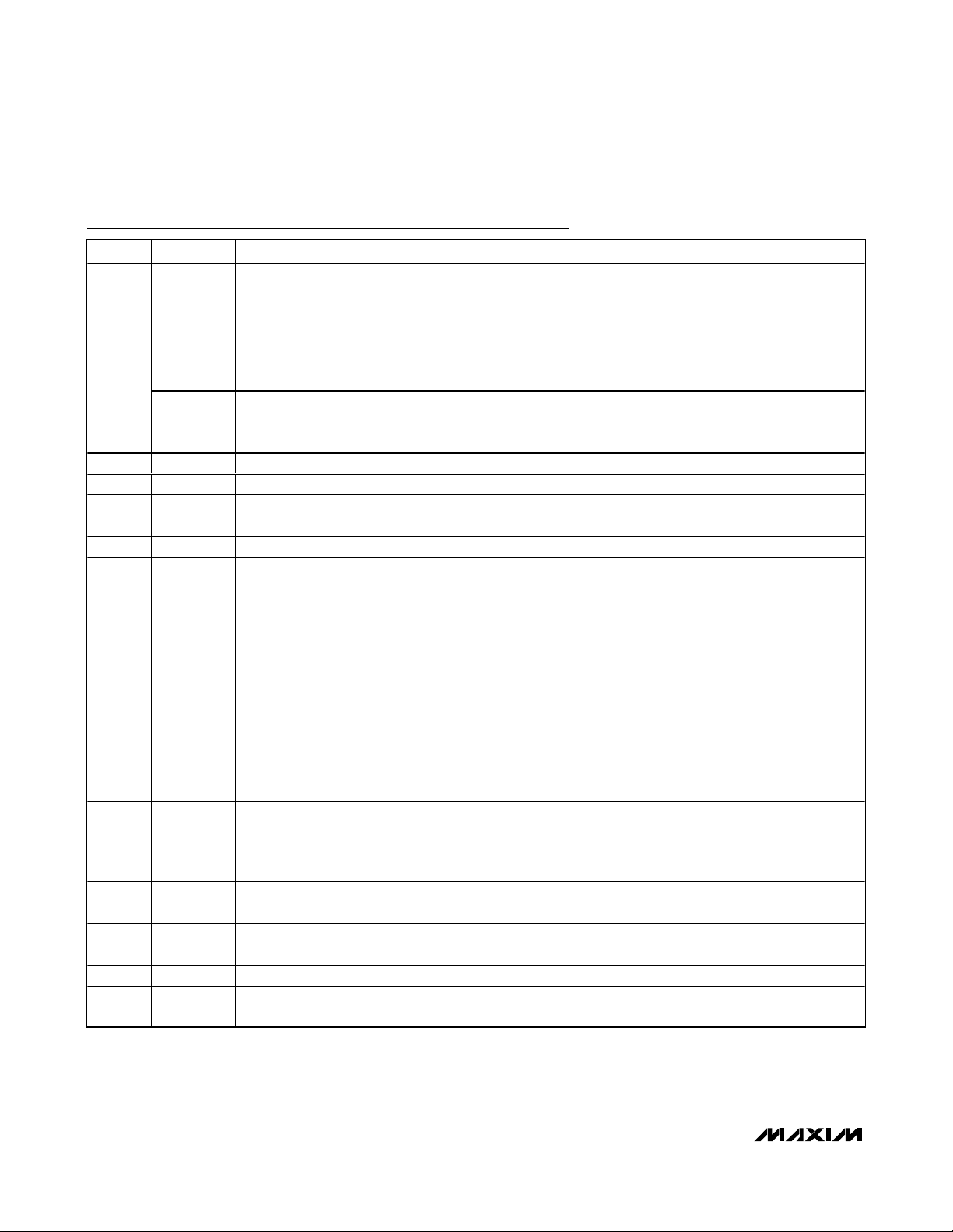
Pin Description (continued)
PIN NAME FUNCTION
10 CCI
11 REF
12 FB
13 GNDS
14 CSP2
CSN12
(MAX8771)
15
Current-Balance Compensation. Connect a 470pF capacitor between CCI and the positive side of the
feedback remote sense (or between CCI and GND). CCI is internally forced low in shutdown.
2.0V Refer ence Outp ut. Byp ass to G N D w i th a 1µF m a x im u m l ow - E S R ( cer am i c) cap aci tor . C an sour ce
500µA for exter nal l oad s. Load i ng RE F d eg r ad es O U T accur acy, accor d i ng to the RE F l oad - r eg ul ati on er r or .
Output of the DC-Voltage Positioning Transconductance Amplifier. Connect a resistor R
the positive side of the feedback remote sense to set the DC steady-state droop based on the voltagepositioning gain requirement:
= R
R
FB
where R
the current-sense resistors that are used to provide the (CSP_, CSN_) current-sense voltages. If lossless
sensing is used, R
thermistor to minimize the temperature dependence of the voltage-positioning slope. DC droop can be
disabled by shorting FB to the positive remote-sense point. FB is high impedance in shutdown.
Feedback Remote-Sense Input, Negative Side. Normally connected to GND directly at the load. GNDS
internally connects to a transconductance amplifier that fine tunes the output voltage— compensating for
voltage drops from the regulator ground to the load ground.
Positive Input of the Output Current Sense of Phase 2. This pin should be connected to the positive side of
the output current-sensing resistor or the filtering capacitor if the DC resistance of the output inductor is
utilized for current sensing. Tie this pin to V
Combined Negative Current-Sense Input for Phases 1 and 2. The negative current-sense signals of the
two phases (taken from the negative sides of the output current-sensing resistors or the filtering capacitors
if the DC resistances of the output inductors are utilized for current sensing) are resistively averaged, and
the resulting signal is connected to this pin. Pay special attention to board layout to maximize currentsensing accuracy; either place the sense elements (inductors for lossless sensing or sense resistors)
close to each other, or equalize the layout paths and PC board trace resistances between the sense
elements and the remote load. CSN12 is also used as the voltage input to the power monitor.
is the desired voltage-positioning slope and G
DROOP
= RL. In this case, consider making R
SENSE
/ (R
DROOP
for 1-phase operation.
CC
SENSE
between FB and
FB
x G
m(FB)
)
m(FB)
= 600µS (typ). R
a resistor network that includes an NTC
FB
SENSE
is the value of
16
CSN2
(MAX8770
/MAX8772)
CSP1
(MAX8771)
CSN1
(MAX8770/
MAX8772)
Negative Input of the Output Current Sense of Phase 2. This pin should be connected to the negative side
of the output current-sensing resistor or the filtering capacitor if the DC resistance of the output inductor is
utilized for current sensing. CSN2 is also used as the voltage input to the power monitor.
Positive Input of the Output Current Sense of Phase 1. This pin should be connected to the positive side of
the output current-sensing resistor or the filtering capacitor if the DC resistance of the output inductor is
utilized for current sensing.
Negative Input of the Output Current Sense of Phase 1. This pin should be connected to the negative side
of the output current-sensing resistor or the filtering capacitor if the DC resistance of the output inductor is
utilized for current sensing.
Page 16
MAX8770/MAX8771/MAX8772
MAX8770/MAX8771/MAX8772 Dual-Phase, Quick-
PWM Controller for IMVP-6+ CPU Core Power Supplies
16 ______________________________________________________________________________________
CONFIDENTIAL INFORMATION – RESTRICTED TO INTEL®IMVP-6 LICENSEES
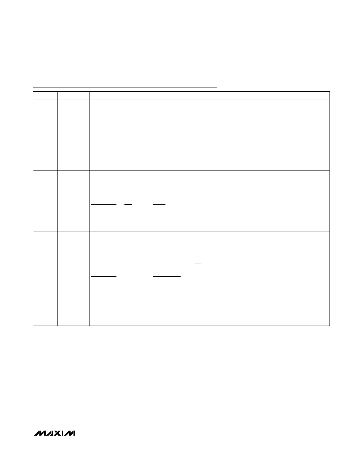
Pin Description (continued)
PIN NAME FUNCTION
Open-Drain, Phase-Good Output. Used to signal the system that one of the two phases either has a fault
condition or is not matched with the other. Detection is done by identifying the need for a large on-time
PHASEGD
(MAX8771)
17
difference between phases in order to achieve or move towards current balance. PHASEGD is low in
shutdown.
PHASEGD is forced high impedance whenever the slew-rate controller is active (output-voltage
transitions).
PHASEGD is forced high impedance while in 1-phase operation (DPRSLPVR = high or PSI = low).
CSP1
(MAX8770
MAX8772)
Positive Input of the Output Current Sense of Phase 1. This pin should be connected to the positive side of
the output current-sensing resistor or the filtering capacitor if the DC resistance of the output inductor is
utilized for current sensing.
18 GND Analog Ground. Connect to the exposed backside pad and low-current analog ground terminations.
19 V
CC
20 BST2
Controller Supply Voltage. Connect to a 4.5V to 5.5V source. Bypass to GND with 1µF minimum.
Boost Flying-Capacitor Connection for the DH2 high-side gate driver. An internal switch between V
BST2 charges the flying capacitor during the time the low-side FET is on.
21 DH2 Phase-2, High-Side Gate-Driver Output. DH2 swings from LX2 to BST2. Low in shutdown.
22 LX2
23 PGND2
Phase-2 Inductor Connection. LX2 is the internal lower supply rail for the DH2 high-side gate driver. Also
used as an input to the phase 2’s zero-crossing comparator.
Power Ground for Phase 2. Ground connection for the DL2 driver. Also used as an input to phase 2’s zero
crossing comparator.
Phase-2, Low-Side Gate-Driver Output. DL2 swings from PGND2 to V
24 DL2
25 V
DD
DL2 is also forced high when an output overvoltage fault is detected, overriding any negative current-limit
condition that may be present. DL2 is forced low in skip mode (DPRSLPVR high) after an inductor current
zero crossing (PGND2 - LX2) is detected. DL2 is forced low in 1-phase mode (TWO - PH = low).
Supply Voltage Input for the DL1 and DL2 Drivers. VDD is also the supply voltage used to internally
recharge the BST1, BST2 flying capacitors during the off-times of the respective phases. Connect V
the 4.5V to 5.5V system supply voltage. Bypass V
ceramic capacitors.
Phase 1, Low-Side Gate-Driver Output. DL1 swings from PGND1 to V
26 DL1
DL1 is also forced high when an output overvoltage fault is detected, overriding any negative current-limit
condition that may be present. DL1 is forced low in skip mode (DPRSLPVR high) whenever an inductor
current zero crossing (PGND1 - LX1) is detected.
. DL2 is forced high in shutdown.
DD
to PGND1 and PGND2 with a 1µF each or greater
DD
. DL1 is forced high in shutdown.
DD
DD
DD
and
to
27 PGND1
28 LX1
Power Ground for Phase 1. Ground connection for the DL1 driver. Also used as an input to the phase 1’s
zero crossing comparator.
Phase 1 Inductor Connection. LX1 is the internal lower supply rail for the DH1 high-side gate driver. Also
used as an input to the phase-1’s zero-crossing comparator.
29 DH1 Phase 1 High-Side Gate-Driver Output. DH1 swings from LX1 to BST1. Low in shutdown.
30 BST1
Boost Flying Capacitor Connection for the DH1 High-Side Gate Driver. An internal switch between V
and BST1 charges the flying capacitor during the time the low-side FET is on.
DD
Page 17
MAX8770/MAX8771/MAX8772
MAX8770/MAX8771/MAX8772 Dual-Phase, Quick-
PWM Controller for IMVP-6+ CPU Core Power Supplies
______________________________________________________________________________________ 17
CONFIDENTIAL INFORMATION – RESTRICTED TO INTEL®IMVP-6 LICENSEES
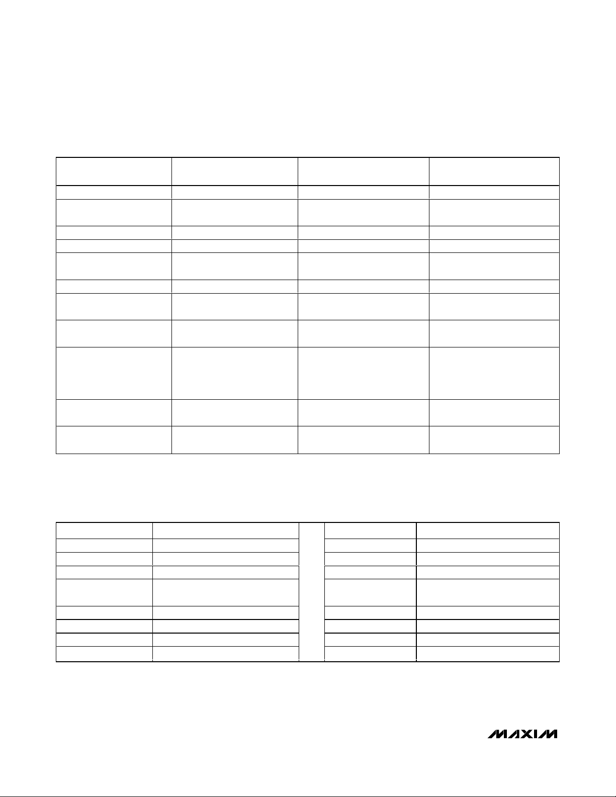
Pin Description (continued)
PIN NAME FUNCTION
Low-Voltage VID DAC Code Input. The D0–D6 inputs do not have internal pullups. These 1.0V logic inputs
31–37 D0–D6
38 SHDN
39 DPRSLPVR
40 DPRSTP
EP EP Exposed Backside Pad. Connect the exposed backside pad to AGND.
are designed to interface directly with the CPU. The output voltage is set by the VID code indicated by the
logic-level voltages on D0–D6 (see Table 4).
Shutdown Control Input. This input cannot withstand the battery voltage. Connect to V
operation. Connect to ground to put the IC into its 1µA max shutdown state. During startup, the output
voltage is ramped up to the boot voltage slowly at a slew rate that is 1/8 the slew rate set by the TIME
resistor. During the transition from normal operation to shutdown, the output voltage is ramped down at the
same slow slew rate. Forcing SHDN to 11V~13V disables both OVP and UVP protection circuits, clears the
fault latch, disables transient phase overlap, and disables the BST_ charging switches. Do not connect
SHDN to > 13V.
Logic Input to Indicate Power Usage. PSI and DPRSLPVR together determine the operating mode as
shown in the truth table below. The PWRGD upper threshold is blanked when the part is in skip mode. The
part is forced into full-phase PWM mode during startup, while in boot mode, during the transition
from boot mode to VID mode, and during shutdown.
DPRSLPVR PSI Mode
1 0 Very low current (1-phase skip)
1 1 Low current (approximately 3A) (1-phase skip)
0 0 Intermediate power potential (1-phase PWM)
0 1 Max power potential (full-phase PWM: number of phases by CSP2)
1.0V Logic-Input Signal. This signal from the system is usually the logical complement of the DPRSLPVR
signal. However, there is a special condition during C4 exit when both DPRSTP and DPRSLPVR could
temporarily be simultaneously high. If this happens, the slew rate reduces to 1/4 of the normal (R
based) slew rate for the duration of this condition. The slew rate returns to normal when this condition is
exited. Note that only DPRSLPVR and PSI (but
skip) and the number of active phases:
DPRSLPVR DPRSTP Functionality
0 0 Normal slew rate, number of phases set by PSI and CSP2
(DPRSLPVR low →→→→ DPRSTP is ignored)
0 1 Normal slew rate, number of phases set by PSI and CSP2
(DPRSLPVR low →→→→ DPRSTP is ignored)
1 0 Normal slew rate, 1-phase skip mode
1 1 Slew rate reduced to 1/4 of normal,1-phase skip mode
not DPRSTP) determine the mode of operation (PWM vs.
for normal
CC
TIME
-
Page 18
MAX8770/MAX8771/MAX8772
MAX8770/MAX8771/MAX8772 Dual-Phase, Quick-
PWM Controller for IMVP-6+ CPU Core Power Supplies
18 ______________________________________________________________________________________
CONFIDENTIAL INFORMATION – RESTRICTED TO INTEL®IMVP-6 LICENSEES
Table 1. Component Selection for Standard Applications
Table 2. Component Suppliers
DESIGNATION
Input Voltage Range 7V to 24V 7V to 24V 7V to 24V
VID Output Voltage
(D6–D0)
Load Line -2.1mV/A -2.1mV/A -5.1mV/A
Maximum Load Current 36A 44A 9A
Inductor (per Phase)
Switching Frequency 300kHz (R
High-Side MOSFET
(N
, per Phase)
H
Low-Side MOSFET
(N
, per Phase)
L
Total Input Capacitance
(C
)
IN
1.2875V/36A COMPONENTS
(FIGURE 1)
1.2875V
(D6–D0 = 0010001)
0.36µH, 0.8mΩ
NEC/Tokin MPC1055LR36
= 200kΩ) 300kHz (R
TON
Siliconix (1) Si7892ADP Siliconix (1) Si7892ADP Siliconix (1) Si7892ADP
Siliconix (2) Si7336ADP Siliconix (2) Si7336ADP Siliconix (1) Si7336ADP
(4) 10µF, 25V
Taiyo Yuden TMK432BJ106KM
or
TDK C4532X5R1E106M
1.1500V/44A COMPONENTS
(FIGURE 1)
1.1500V
(D6–D0 = 0011100)
0.33µH, 0.82mΩ
Panasonic ETQP5LR33XFC
= 200kΩ) 300kHz (R
TON
(4) 10µF, 25V
Taiyo Yuden TMK432BJ106KM
or
TDK C4532X5R1E106M
0.9000V/9A COMPONENTS
(FIGURE 12)
0.9000V
(D6–D0 = 0110000)
0.56µH, 1.3mΩ
NEC/Tokin MPC1040LR56
= 200kΩ)
TON
(2) 10µF, 25V
Taiyo Yuden TMK432BJ106KM
or
TDK C4532X5R1E106M
Total Output Capacitance
(C
)
OUT
Current-Sense Resistor
(R
, per Phase)
CS
(4) 330µF, 2.5V, 6mΩ
Panasonic EEFSX0D0D331XR
1.0mΩ
Panasonic ERJM1WTJ1M0U
(4) 330µF, 2.5V, 6mΩ
Panasonic EEFSX0D0D331XR
1.0mΩ
Panasonic ERJM1WTJ1M0U
(2) 330µF, 2.5V, 6mΩ
Panasonic EEFSX0D0D331XR
Panasonic ERJM1WTJ2M0U
MANUFACTURER WEBSITE MANUFACTURER WEBSITE
AVX www.avxcorp.com Pulse www.pulseeng.com
BI Technologies www.bitechnologies.com Renesas www.renesas.com
Central Semiconductor www.centralsemi.com Sanyo www.secc.co.jp
Fairchild
Semiconductor
International Rectifier www.irf.com Sumida www.sumida.com
Kemet www.kemet.com Taiyo Yuden www.t-yuden.com
NEC/Tokin www.nec-tokin.com TDK www.component.tdk.com
Panasonic www.panasonic.com TOKO www.tokoam.com
www.fairchildsemi.com Siliconix (Vishay) www.vishay.com
2.0mΩ
Page 19
MAX8770/MAX8771/MAX8772
MAX8770/MAX8771/MAX8772 Dual-Phase, Quick-
PWM Controller for IMVP-6+ CPU Core Power Supplies
______________________________________________________________________________________ 19
CONFIDENTIAL INFORMATION – RESTRICTED TO INTEL®IMVP-6 LICENSEES
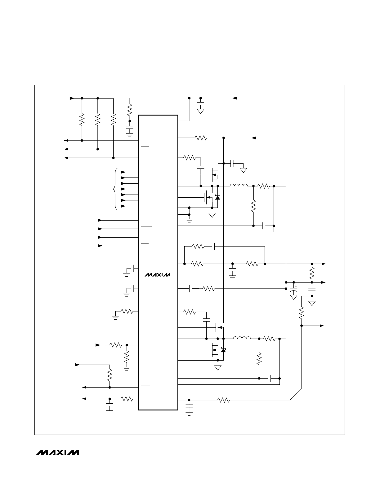
Figure 1. Standard 2-Phase IMVP-6 44A Application Circuit
R17
100
5V BIAS
SUPPLY
INPUT V
IN
8V TO 24V
C
IN
RCS1
L1
C8
4700pF
1mΩ
R12
100Ω
C11
2.2nF
R10
100Ω
RCS1
R12
100Ω
1mΩ
C11
2.2nF
L1
* CSN1 and CSN2 are bonded together on the
MAX8771 and called CSN12
** Optional -- Resistor allow remote sensing for system
verification when the CPU is not present
+ PHASEGD is only on the MAX8771
CPU V
CC
SENSE
R11**
10Ω
OUTPUT
C
OUT
R16**
10Ω
CPU GND
SENSE
3.3V BIAS
CLK_ENABLE#
IMVPOK
SUPPLY
1.2V BIAS
SUPPLY
10kΩ
R4
DPRLSPVR
1.9kΩ
PSI#
DPRSTP#
VR_ON
CC
R3
DAC INPUTS
(1V LOGIC)
56Ω
C10
0.1µF
1.9kΩ
R7
C1
3.40kΩ
C7
200kΩ
R18
0Ω
R9
C9
4700pF
R18
N
C3
0.22µF
N
L1
N
2.2µF
H1
R18
0Ω
L2
C13
OPEN
N
H2
R1
10Ω
R2
C2
2.2µF
C5
470pF
C6
0.1µF
71.5kΩ
R6
13kΩ
NTC4
100kΩ
R5
R8
10kΩ
V
CC
PHASEGD
CLKEN
PWRGD
D0
D1
D2
D3
D4
D5
D6
PSI
DPRSTP
DPRSLPVR
SHDN
CCV
MAX8770
MAX8771
REF
MAX8772
TIME
THRMV
VRHOT
POUT
V
RTON
BST1
DH1
DL1
PGND1
GND
CSP1
*CSN1
CCI
BST2
DH2
LX2
DL2
PGND2
CSP2
*CSN2
GNDS
LX1
DD
R22
0Ω
FB
470pF
R23
0Ω
Page 20
MAX8770/MAX8771/MAX8772
MAX8770/MAX8771/MAX8772 Dual-Phase, Quick-
PWM Controller for IMVP-6+ CPU Core Power Supplies
20 ______________________________________________________________________________________
CONFIDENTIAL INFORMATION – RESTRICTED TO INTEL®IMVP-6 LICENSEES
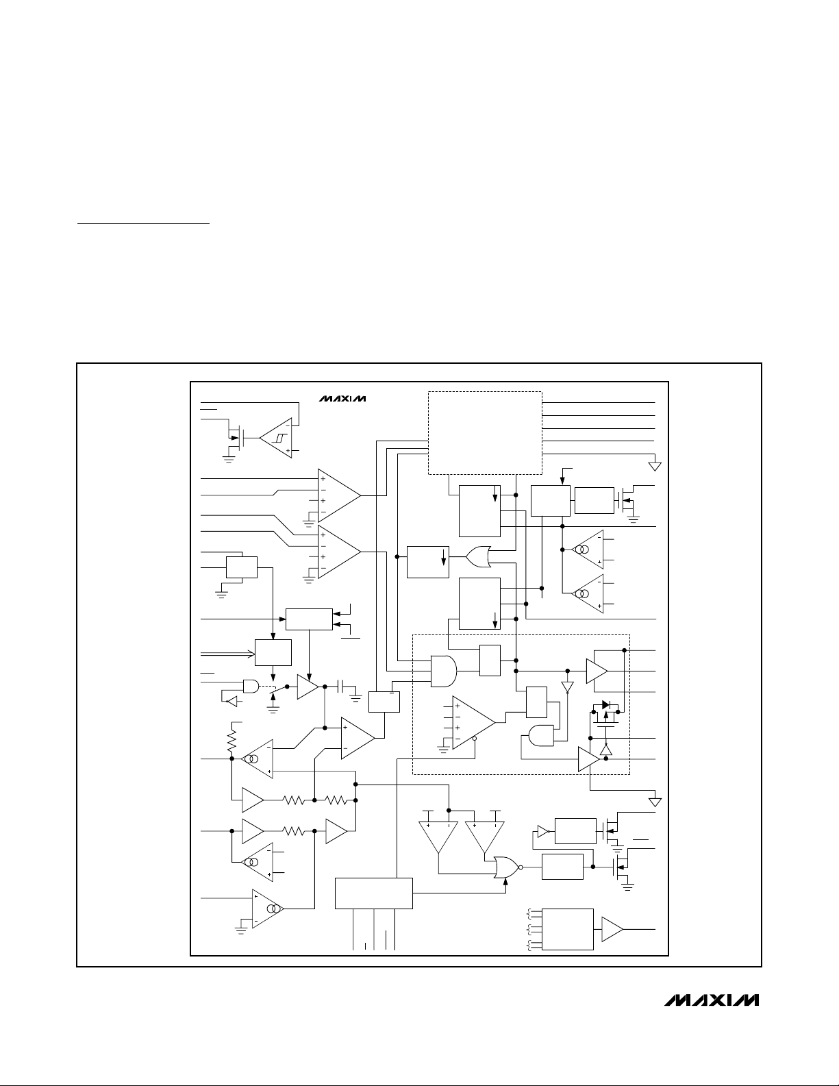
Figure 2. Functional Block Diagram
MAX8770/MAX8771/MAX8772
Detailed Description
Free-Running, Constant On-Time PWM
Controller with Input Feed-Forward
The Quick-PWM control architecture is a pseudo-fixedfrequency, constant-on-time, current-mode regulator
with voltage feed-forward (Figure 2). This architecture
relies on the output filter capacitor’s ESR to act as the
current-sense resistor, so the output ripple voltage pro-
vides the PWM ramp signal. The control algorithm is simple: the high-side switch on-time is determined solely by
a one-shot whose period is inversely proportional to
input voltage, and directly proportional to output voltage
or the difference between the main and secondary
inductor currents (see the On-Time One-Shot section).
Another one-shot sets a minimum off-time. The on-time
one-shot triggers when the error comparator goes low,
the inductor current of the selected phase is below the
valley current-limit threshold, and the minimum off-time
one-shot times out. The controller maintains 180° out-of-
THRM
VRHOT
CSP2
CSN2
CSP1
CSN1
VCC
REF
REF
(2.0V)
GND
TIME
D0–D6
SHDN
CCV
FB
GNDS
Gm(CCV)
(FB)
G
m
FAULT
REF
x2
DAC
CSP_
CSN_
0.3 x V
22.5mV
22.5mV
R-TO-I
CONVERTER
CC
TARGET
MAX8770
MAX8771
MAX8772
DPRSLPVR
DPRSTP
QQ
PHASE CONTROL
DPRSLPVR
PSI
T
Q
MINIMUM
OFF-TIME
TRIG
Q
ONE-SHOT
Q
CSP1
CSN1
2.5mV
TARGET
- 300mV
SKIP
BLANK
DPRSTP
SECONDARY
PHASE DRIVERS
TRIG
ONE-SHOT
PHASE 2
ON-TIME
PHASE 1
ON-TIME
ONE-SHOT
TRIG
R
Q
S
SKIP
TARGET
+ 200mV
CSP1 - CSN1
CSN1 - GNDS
CSP2 - CSN2
CURRENTBALANCE-
FAULT
FB
MAIN PHASE
DRIVERS
S
Q
R
STARTUP
60µs
STARTUP
DELAY
POWER
MONITOR
G
m
G
m
5ms
DELAY
BLANK
(CCI)
(CCI)
5ms
STARTUP
DELAY
CSN2
CSP2
CSP1
CSN1
BST2
DH2
PGND2
PHASEGD
TON
BST1
PGND1
PWRGD
CLKEN
POUT
LX2
DL2
CCI
DH1
LX1
V
DD
DL1
Page 21

MAX8770/MAX8771/MAX8772
MAX8770/MAX8771/MAX8772 Dual-Phase, Quick-
PWM Controller for IMVP-6+ CPU Core Power Supplies
______________________________________________________________________________________ 21
CONFIDENTIAL INFORMATION – RESTRICTED TO INTEL®IMVP-6 LICENSEES
phase operation by alternately triggering the main and
secondary phases after the error comparator drops
below the output voltage set point.
Dual 180° Out-of-Phase Operation
The two phases in the MAX8770/MAX8771/MAX8772
operate 180° out-of-phase to minimize input and output
filtering requirements, reduce electromagnetic interference (EMI), and improve efficiency. This effectively lowers component count—reducing cost, board space,
and component power requirements— making the
MAX8770/MAX8771/MAX8772 ideal for high-power,
cost-sensitive applications.
Typically, switching regulators provide power using
only 1 phase instead of dividing the power among several phases. In these applications, the input capacitors
must support high instantaneous current requirements.
The high RMS ripple current can lower efficiency due to
I2R® power loss associated with the input capacitor’s
effective series resistance (ESR). Therefore, the system
typically requires several low-ESR input capacitors in
parallel to minimize input voltage ripple, to reduce ESRrelated power losses, and to meet the necessary RMS
ripple current rating.
With the MAX8770/MAX8771/MAX8772, the controller
shares the current between two phases that operate
180° out-of-phase, so the high-side MOSFETs never
turn on simultaneously during normal operation. The
instantaneous input current of either phase is effectively
halved, resulting in reduced input voltage ripple, ESR
power loss, and RMS ripple current (see the Input
Capacitor Selection section). Therefore, the same performance may be achieved with fewer or less-expensive input capacitors.
+5V Bias Supply (VCCand VDD)
The Quick-PWM controller requires an external +5V
bias supply in addition to the battery. Typically, this
+5V bias supply is the notebook’s 95% efficient +5V
system supply. Keeping the bias supply external to the
IC improves efficiency and eliminates the cost associated with the +5V linear regulator that would otherwise be
needed to supply the PWM circuit and gate drivers. If
stand-alone capability is needed, the +5V bias supply
can be generated with an external linear regulator.
The +5V bias supply must provide VCC(PWM controller) and VDD(gate-drive power), so the maximum
current drawn is:
I
BIAS
= ICC- fSW(Q
G(LOW)
+ Q
G(HIGH)
)
where ICCis provided in the Electrical Characteristics
Table, fSWis the switching frequency, and Q
G(LOW)
and Q
G(HIGH)
are the MOSFET data sheet’s total gate-
charge specification limits at VGS= 5V.
VINand VDDcan be tied together if the input power
source is a fixed +4.5V to +5.5V supply. If the +5V
bias supply is powered up prior to the battery supply,
the enable signal (SHDN going from low to high) must
be delayed until the battery voltage is present to
ensure startup.
Switching Frequency (TON)
Connect a resistor (R
TON
) between TON and VINto set
the switching period TSW= 1/fSW, per phase:
TSW= C
TON(RTON
+ 6.5kΩ)
where C
TON
= 16.26pF.
A 96.75kΩ to 303.25kΩ corresponds to switching periods of 167ns (600kHz) to 500ns (200kHz), respectively.
High-frequency (600kHz) operation optimizes the application for the smallest component size, trading off efficiency due to higher switching losses. This may be
acceptable in ultra-portable devices where the load
currents are lower and the controller is powered from a
lower voltage supply. Low-frequency (200kHz) operation offers the best overall efficiency at the expense of
component size and board space.
On-Time One-Shot
The core of each phase contains a fast, low-jitter,
adjustable one-shot that sets the high-side MOSFETs
on-time. The one-shot for the main phase varies the ontime in response to the input and feedback voltages.
The main high-side switch on-time is inversely proportional to the input voltage (VIN), and proportional to the
feedback voltage (VFB):
where the switching period (TSW= 1/fSW) is set by the
resistor at the TON pin, and 0.075V is an approximation
to accommodate the expected drop across the lowside MOSFET switch.
The one-shot for the secondary phase varies the ontime in response to the input voltage and the difference
between the main and secondary inductor currents.
Two identical transconductance amplifiers integrate the
difference between the master and slave current-sense
signals. The summed output is internally connected to
I2R is a registered trademark of instruments for Research and
Industry, Inc.
TV V
t
()
ON MAIN
=
SW FB
0 075
.
+
()
V
IN
Page 22

MAX8770/MAX8771/MAX8772
MAX8770/MAX8771/MAX8772 Dual-Phase, Quick-
PWM Controller for IMVP-6+ CPU Core Power Supplies
22 ______________________________________________________________________________________
CONFIDENTIAL INFORMATION – RESTRICTED TO INTEL®IMVP-6 LICENSEES
CCI, allowing adjustment of the integration time constant with a compensation network connected between
CCI and FB. The resulting compensation current and
voltage are determined by the following equations:
I
CCI
= GM(V
CMP
- V
CMN
) - GM(V
CSP
- V
CSN
)
V
CCI
= VFB+ I
CCIZCCI
where Z
CCI
is the impedance at the CCI output. The
secondary on-time one-shot uses this integrated signal
(V
CCI
) to set the secondary high-side MOSFETs ontime. When the main and secondary current-sense signals (VCM= V
CMP
- V
CMN
and VCS= V
CSP-VCSM
)
become unbalanced, the transconductance amplifiers
adjust the secondary on-time, which increases or
decreases the secondary inductor current until the current-sense signals are properly balanced:
= (Main On-Time)
+ (Secondary Current Balance Correction)
This algorithm results in a nearly constant switching frequency and balanced inductor currents, despite the lack
of a fixed-frequency clock generator. The benefits of a
constant switching frequency are twofold: first, the frequency can be selected to avoid noise-sensitive regions
such as the 455kHz IF band; second, the inductor ripplecurrent operating point remains relatively constant,
resulting in easy design methodology and predictable
output voltage ripple. The on-time one-shots have good
accuracy at the operating points specified in the
Electrical Characteristics table. On-times at operating
points far removed from the conditions specified in the
Electrical Characteristics table can vary over a wider
range. For example, the 600kHz setting typically runs
about 5% slower, with inputs much greater than +12V
due to the very short on-times required.
On-times translate only roughly to switching frequencies. The on-times guaranteed in the Electrical
Characteristics table are influenced by switching
delays in the external high-side MOSFET. Resistive
losses, including the inductor, both MOSFETs, output
capacitor ESR, and PC board copper losses in the output and ground tend to raise the switching frequency at
higher output currents. Also, the dead-time effect
increases the effective on-time, reducing the switching
frequency. It occurs only during forced-PWM operation
and dynamic output-voltage transitions when the induc-
tor current reverses at light or negative load currents.
With reversed inductor current, the inductor’s EMF
causes LX to go high earlier than normal, extending the
on-time by a period equal to the DH-rising dead time.
For loads above the critical conduction point, where the
dead-time effect is no longer a factor, the actual switching frequency (per phase) is:
where V
DIS
is the sum of the parasitic voltage drops in
the inductor discharge path, including synchronous
rectifier, inductor, and PC board resistances; V
CHG
is
the sum of the parasitic voltage drops in the inductor
charge path, including high-side switch, inductor, and
PC board resistances; and tONis the on-time as determined above.
Current Sense
The output current of each phase is sensed. Low-offset
amplifiers are used for current balance, voltage-positioning gain, and current limit. Sensing the current at
the output of each phase offers advantages, including
less noise sensitivity, more accurate current sharing
between phases, and the flexibility of using either a
current-sense resistor or the DC resistance of the output inductor.
Using the DC resistance (R
DCR
) of the output inductor
allows higher efficiency. In this configuration, the initial
tolerance and temperature coefficient of the inductor’s
DCR must be accounted for in the output-voltage
droop-error budget and power monitor. This currentsense method uses an RC filtering network to extract
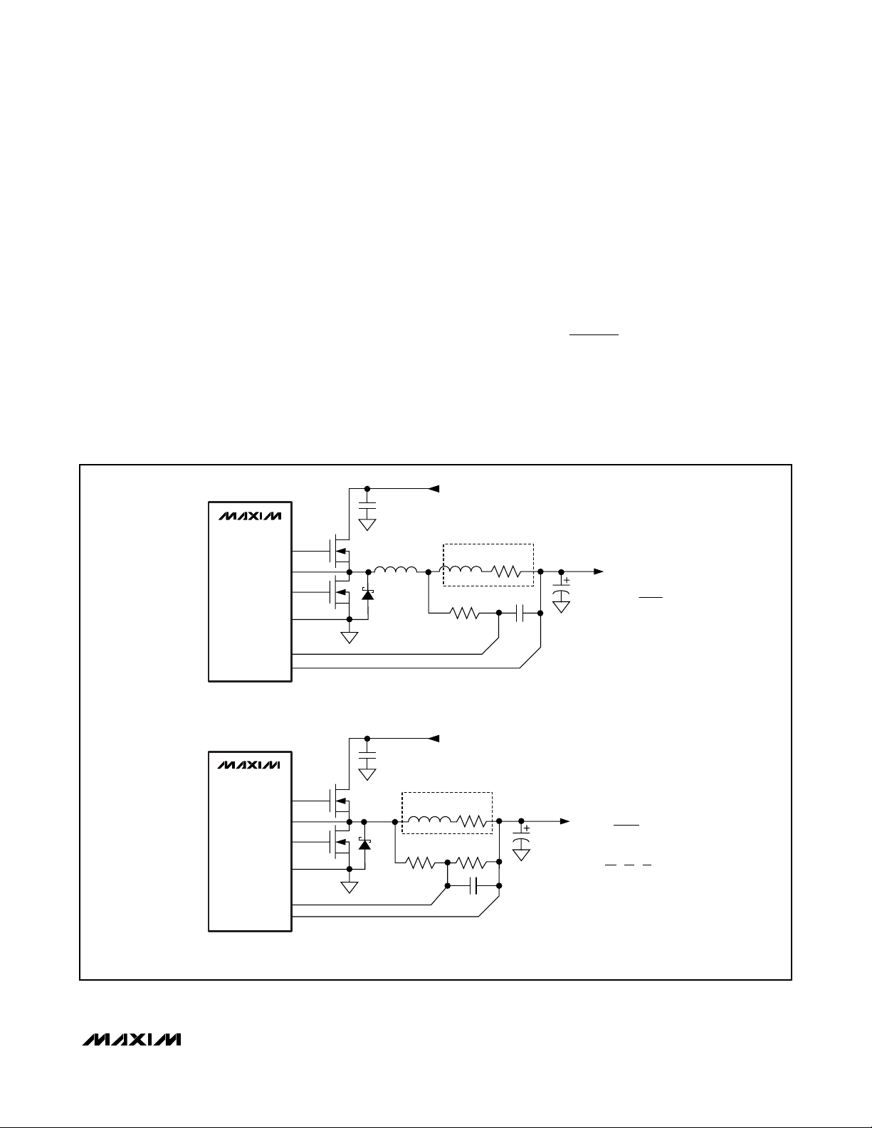
the current information from the output inductor (see
Figure 3). The resistive divider used should provide a
current-sense resistance (RCS) low enough to meet the
current-limit requirements, and the time constant of the
RC network should match the inductor’s time constant
(L/RCS):
where R
CS
is the required current-sense resistance,
and R
DCR
is the inductor’s series DC resistance. Use
the worst-case inductance and R
DCR
values provided
by the inductor manufacturer, adding some margin for
the inductance drop over temperature and load. To
()
tT
ON SEC SW
=
()
=
⎛
VV
CCI
⎜
⎝
⎛
VV
FB
T
SW
⎜
⎝
.
+
0 075
V
IN
.
+
0 075
V
IN
⎞
⎟
⎠
⎞
⎟
⎠
⎛
IZ
CCI CCI
T
+
SW
⎜
⎝
⎞
⎟
V
⎠
IN
VV
+
OUT DIS
f
SW
()
=
tVV V
ON IN DIS CHG
+−
R
2
⎛
R
=
⎜
CS DCR
⎝
R
=+
CS
CRR
+
RR
12
L
111
⎡
⎢
⎣
EQ
⎞
R and
⎟
⎠
⎤
⎥
2
⎦
Page 23
MAX8770/MAX8771/MAX8772
MAX8770/MAX8771/MAX8772 Dual-Phase, Quick-
PWM Controller for IMVP-6+ CPU Core Power Supplies
______________________________________________________________________________________ 23
CONFIDENTIAL INFORMATION – RESTRICTED TO INTEL®IMVP-6 LICENSEES
minimize the current-sense error due to the currentsense inputs’ bias current (I
CSP
_ and I
CSN
_), choose
R1||R2 to be less than 2kΩ and use the above equation
to determine the sense capacitance (CEQ). Choose
capacitors with 5% tolerance and resistors with 1% tolerance specifications. Temperature compensation is
recommended for this current-sense method. See the
Voltage Positioning and the Loop Compensation section for detailed information.
When using a current-sense resistor for accurate output-voltage positioning, the circuit requires a differential
RC filter to eliminate the AC voltage step cause by the
equivalent series inductance (L
ESL
) of the currentsense resistor (see Figure 3). The ESL-induced voltage
step does not affect the average current-sense voltage,
but results in a significant peak current-sense voltage
error that results in unwanted offsets in the regulation
voltage and results in early current-limit detection.
Similar to the inductor DCR sensing method above, the
RC filter’s time constant should match the L/R time constant formed by the current-sense resistor’s parasitic
inductance:
where L
ESL
is the equivalent series inductance of the
current-sense resistor, R
SENSE
is current-sense resistance value, and CEQand REQare the time-constant
matching components.
Figure 3. Current-Sense Methods
C
IN
N
DH_
LX_
DL_
PGND
CSP_
CSN_
H
L
D
N
L
L
L
ESL
= 1
CR
EQ
R
SENSE
)
INPUT (V
IN
SENSE RESISTOR
L
ESLRSENSE
CEQR1 =
L
SENSE
R
SENSE
C
OUT
R1
C
EQ
A) OUTPUT SERIES RESISTOR SENSING
B) LOSSLESS INDUCTOR SENSING
DH_
LX_
DL_
PGND
CSP_
CSN_
INPUT (V
)
DCR
IN
R2
R1 + R2
L
R1 R2C
[ + ]
EQ
R
DCR
11
R
=
CS
R
DCR
( )
=
C
R2
C
EQ
OUT
C
IN
N
H
D
N
L
L
INDUCTOR
L
R1
FOR THERMAL COMPENSATION:
R2 SHOULD CONSIST OF AN NTC RESISTOR IN
SERIES WITH A STANDARD THIN-FILM RESISTOR
Page 24

MAX8770/MAX8771/MAX8772
MAX8770/MAX8771/MAX8772 Dual-Phase, Quick-
PWM Controller for IMVP-6+ CPU Core Power Supplies
24 ______________________________________________________________________________________
CONFIDENTIAL INFORMATION – RESTRICTED TO INTEL®IMVP-6 LICENSEES
Current Balance
Without active current-balance circuitry, the current
matching between phases depends on the MOSFETs’
on-resistance (R
DS(ON)
), thermal ballasting, on/off-time
matching, and inductance matching. For example, variation in the low-side MOSFET on-resistance (ignoring
thermal effects) results in a current mismatch that is
proportional to the on-resistance difference:
However, mismatches between on-times, off-times, and
inductor values increase the worst-case current imbalance, making it impossible to passively guarantee
accurate current balancing.
The MAX8770/MAX8771/MAX8772 integrate the difference between the current-sense voltages and adjust the
on-time of the secondary phase to maintain current balance. The current balance now relies on the accuracy of
the current-sense resistors instead of the inaccurate, thermally sensitive on-resistance of the low-side MOSFETs.
With active current balancing, the current mismatch is
determined by the current-sense resistor values and the
offset voltage of the transconductance amplifiers:
where R
SENSE
= RCM= RCSand V
OS(IBAL)
is the current-balance offset specification in the Electrical
Characteristics table .
The worst-case current mismatch occurs immediately
after a load transient due to inductor value mismatches
resulting in different di/dt for the two phases. The time it
takes the current-balance loop to correct the transient
imbalance depends on the mismatch between the
inductor values and switching frequency.
Current Limit
The current-limit circuit employs a unique “valley” current-sensing algorithm that uses current-sense resistors
between the current-sense inputs (CSP_ to CSN12 for
MAX8771, CSP_ to CSN_ for MAX8770/MAX8772) as
the current-sensing elements. If the current-sense signal of the selected phase is above the current-limit
threshold, the PWM controller does not initiate a new
cycle until the inductor current of the selected phase
drops below the valley current-limit threshold. When
either phase trips the current limit, both phases are
effectively current limited since the interleaved controller does not initiate a cycle with either phase.
Since only the valley current is actively limited, the actual peak current is greater than the current-limit threshold
by an amount equal to the inductor ripple current.
Therefore, the exact current-limit characteristic and
maximum load capability are a function of the currentsense resistance, inductor value, and battery voltage.
When combined with the UVP circuit, this current-limit
method is effective in almost every circumstance.
The positive current-limit threshold is fixed internally at
22.5mV. There is also a negative current limit that prevents excessive reverse inductor currents when V
OUT
is sinking current. The negative current-limit threshold
is set at -30mV. When a phase drops below the negative current limit, the controller immediately activates an
on-time pulse—DL turns off, and DH turns on—allowing
the inductor current to remain above the negative current threshold.
Carefully observe the PC board layout guidelines to
ensure that noise and DC errors do not corrupt the current-sense signals seen by the current-sense inputs
(CSP_, CSN_). For the MAX8771, where the negative
current-sense returns are to a common pin, it is recommended that the current-sense elements (sense resistor or inductor DCR) be placed close to each other to
minimize any voltage differences that might arise due
to trace impedance between the two common nodes.
Feedback Adjustment Amplifiers
Voltage-Positioning Amplifier
(Steady-State Droop)
The MAX8770/MAX8771/MAX8772 include a transconductance amplifier for adding gain to the voltage-positioning sense path. The amplifier’s input is generated
by summing the current-sense inputs, which differentially sense the voltage across either current-sense
resistors or the inductor’s DCR. The amplifier’s output
connects directly to the regulator’s voltage-positioned
feedback input (FB), so the resistance between FB and
the output-voltage sense point determines the voltagepositioning gain:
V
OUT
= V
TARGET
- RFBI
FB
where the target voltage (V
TARGET
) is defined in the
Nominal Output Voltage Selection section, and the FB
amplifier’s output current (IFB) is determined by the
sum of the current-sense voltages:
where VCS= V
CSP
- V
CSN
is the differential current-
sense voltage, and G
m(FB)
is typically 600µS as defined
in the Electrical Characteristics table.
III
MAIN SEC MAIN
III
OS IBAL LMAIN LSEC
()
⎡
⎛
R
−= −
=−=
1
⎢
⎢
⎣
MAIN
⎜
R
⎝
SEC
V
OS IBAL
R
SENSE
()
⎤
⎞
⎥
⎟
⎠
⎥
⎦
IG V
=
FB m FB CSX
()
η
PH
∑
X
=
1
Page 25

MAX8770/MAX8771/MAX8772
MAX8770/MAX8771/MAX8772 Dual-Phase, Quick-
PWM Controller for IMVP-6+ CPU Core Power Supplies
______________________________________________________________________________________ 25
CONFIDENTIAL INFORMATION – RESTRICTED TO INTEL®IMVP-6 LICENSEES
Differential Remote Sense
The MAX8770/MAX8771/MAX8772 include differential,
remote-sense inputs to eliminate the effects of voltage
drops along the PC board traces and through the
processor’s power pins. The feedback-sense node
connects to the voltage-positioning resistor (RFB). The
ground-sense (GNDS) input connects to an amplifier
that adds an offset directly to the target voltage, effectively adjusting the output voltage to counteract the
voltage drop in the ground path. Connect the voltagepositioning resistor (RFB), and ground sense (GNDS)
input directly to the processor’s remote-sense outputs
as shown in Figure 1.
Integrator Amplifier
An integrator amplifier forces the DC average of the FB
voltage to equal the target voltage. This transconductance amplifier integrates the feedback voltage and provides a fine adjustment to the regulation voltage (Figure
2), allowing accurate DC output-voltage regulation
regardless of the output ripple voltage. The integrator
amplifier has the ability to shift the output voltage by
±60mV (typ), including DC offset and AC ripple. The integration time constant can be set easily with an external
compensation capacitor at the CCV pin. Use a 470pF x
(2/η
TOTAL
) x 300kHz/fSWor greater ceramic capacitor.
The MAX8770/MAX8771/MAX8772 disable the integrator by connecting the amplifier inputs together at the
beginning of all VID transitions done in pulse-skipping
mode (DPRSLPVR = high). The integrator remains disabled until 20µs after the transition is completed (the
internal target settles) and the output is in regulation
(edge detected on the error comparator).
Transient-Overlap Operation
When a transient occurs, the response time of the controller depends on how quickly it can slew the inductor
current. Multiphase controllers that remain 180° out-of-
phase when a transient occurs actually respond slower
than an equivalent single-phase controller. In order to
provide fast transient response, the MAX8770/
MAX8771/MAX8772 support a phase-overlap mode that
allows the dual regulators to operate in-phase when
heavy load transients are detected, effectively reducing
the response time. After either high-side MOSFET turns
off, if the output voltage does not exceed the regulation
voltage when the minimum off-time expires, the controller
simultaneously turns on both high-side MOSFETs during
the next on-time cycle. This maximizes the total inductor
current slew rate. The phases remain overlapped until
the output voltage exceeds the regulation voltage after
the minimum off-time expires.
After the phase-overlap mode ends, the controller
automatically begins with the opposite phase. For
example, if the secondary phase provided the last ontime pulse before overlap operation began, the controller starts switching with the main phase when
overlap operation ends.
Nominal Output-Voltage Selection
The nominal no-load output voltage (V
TARGET
) is
defined by the selected voltage reference (VID DAC)
plus the remote ground-sense adjustment (V
GNDS
), as
defined in the following equation:
where V
DAC
is the selected VID voltage. On startup, the
MAX8770/MAX8771/MAX8772 slew the target voltage
from ground to the preset boot voltage.
DAC Inputs (D0–D6)
The digital-to-analog converter (DAC) programs the output voltage using the D0–D6 inputs. D0–D6 are low-voltage (1.0V) logic inputs, designed to interface directly
with the CPU. Do not leave D0–D6 unconnected.
Changing D0–D6 initiates a transition to a new outputvoltage level. Change D0–D6 together, avoiding greater
than 20ns skew between bits. Otherwise, incorrect DAC
readings may cause a partial transition to the wrong voltage level followed by the intended transition to the correct voltage level, lengthening the overall transition time.
The available DAC codes and resulting output voltages
are compatible with the IMVP-6 (Table 4) specifications.
VVVV
TARGET FB DAC GNDS
== +
Page 26

MAX8770/MAX8771/MAX8772
MAX8770/MAX8771/MAX8772 Dual-Phase, Quick-
PWM Controller for IMVP-6+ CPU Core Power Supplies
26 ______________________________________________________________________________________
CONFIDENTIAL INFORMATION – RESTRICTED TO INTEL®IMVP-6 LICENSEES
Table 3. Operating Mode Truth Table
*Multiphase operation = All enabled phases active.
INPUTS
SHDN DPRSTP DPRSLPVR PSI
Low X X X DISABLED
PHASE
OPERATION*
OPERATING MODE
Low-Power Shutdown Mode. DL1 and DL2 forced high,
and the controller is disabled. The supply current drops to
1µA (max).
Multiphase
Rising X X X
High X Low High
High X Low Low
High Low High X
High High High X
forced PWM
R
1/8
TIME
rate
Multiphase
forced PWM;
normal R
slew rate
1-phase forced
PWM;
normal R
slew rate
1-phase pulse
skipping,
normal R
slew rate
1-phase pulse
skipping,
1/4 R
TIME
rate
Startup/Boot. When SHDN is pulled high, the
MAX8770/MAX8771/MAX8772 begin the startup sequence.
Once the REF is above 1.84V, the controller enables the PWM
slew
controller and ramps the output voltage up to the boot
voltage. See Figure 9.
Full Power. The no-load output voltage is determined by the
selected VID DAC code (D0–D6, Table 4).
TIME
Intermediate Power. The no-load output voltage is determined
by the selected VID DAC code (D0–D6, Table 4). When PSI is
pulled low, the MAX8770/MAX8771/MAX8772 immediately
TIME
disable phase 2—DH2, and DL2 pulled low.
Deeper Sleep Mode. The no-load output voltage is
determined by the selected VID DAC code (D0–D6, Table 4).
When DPRSLPVR is pulled high, the MAX8770/MAX8771/
MAX8772 immediately enter 1-phase pulse-skipping
TIME
operation allowing automatic PWM/PFM switchover under
light loads. The PWRGD and CLKEN upper thresholds are
blanked. DH2 and DL2 are pulled low.
Deeper Sleep Slow-Exit Mode. The no-load output voltage is
determined by the selected VID DAC code (D0–D6, Table 4).
When DPRSTP is pulled high while DPRSLPVR is already
high, the MAX8770/MAX8771/MAX8772 remain in 1-phase
slew
pulse-skipping operation, allowing automatic PWM/PFM
switchover under light loads. The PWRGD and CLKEN upper
thresholds are blanked. DH2 and DL2 are pulled low.
Shutdown. When SHDN is pulled low, the
Multiphase
Falling X X X
High X X X DISABLED
forced-PWM,
R
1/8
TIME
rate
MAX8770/MAX8771/MAX8772 immediately pull PWRGD and
PHASEGD low, CLKEN becomes high impedance, all
slew
enabled phases are activated, and the output voltage is
ramped down to ground. Once the output reaches zero, the
controller enters the low-power shutdown state. See Figure 9.
Fault Mode. The fault latch has been set by the MAX8770/
MAX8771/MAX8772 UVP or thermal shutdown protection, or
by the MAX8771 OVP protection. The controller remains in
FAULT mode until V
power is cycled or SHDN toggled.
CC
Page 27
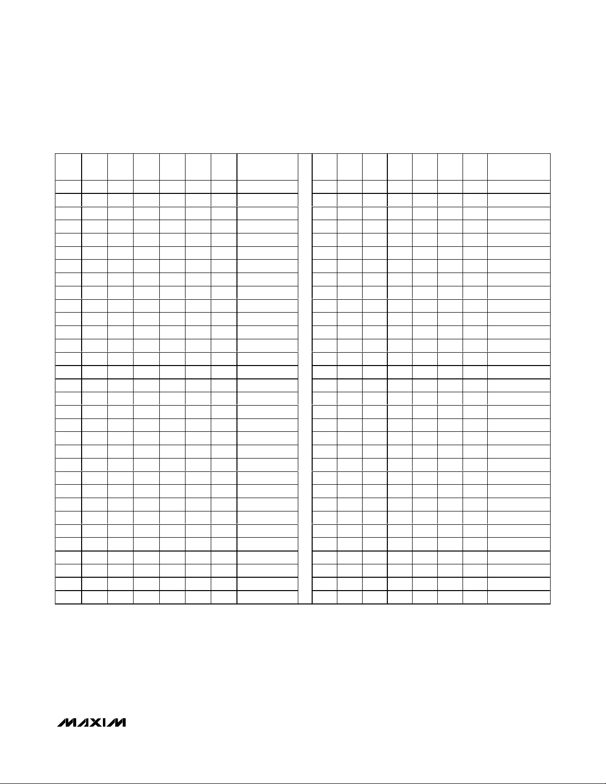
MAX8770/MAX8771/MAX8772
MAX8770/MAX8771/MAX8772 Dual-Phase, Quick-
PWM Controller for IMVP-6+ CPU Core Power Supplies
______________________________________________________________________________________ 27
CONFIDENTIAL INFORMATION – RESTRICTED TO INTEL®IMVP-6 LICENSEES
Table 4. IMVP-6 Output Voltage VID DAC Codes
D6 D5 D4 D3 D2 D1 D0
0000000 1.5000 1000000 0.7000
0000001 1.4875 1000001 0.6875
0000010 1.4750 1000010 0.6750
0000011 1.4625 1000011 0.6625
0000100 1.4500 1000100 0.6500
0000101 1.4375 1000101 0.6375
0000110 1.4250 1000110 0.6250
0000111 1.4125 1000111 0.6125
0001000 1.4000 1001000 0.6000
0001001 1.3875 1001001 0.5875
0001010 1.3750 1001010 0.5750
0001011 1.3625 1001011 0.5625
0001100 1.3500 1001100 0.5500
0001101 1.3375 1001101 0.5375
0001110 1.3250 1001110 0.5250
0001111 1.3125 1001111 0.5125
0010000 1.3000 1010000 0.5000
0010001 1.2875 1010001 0.4875
0010010 1.2750 1010010 0.4750
0010011 1.2625 1010011 0.4625
0010100 1.2500 1010100 0.4500
0010101 1.2375 1010101 0.4375
0010110 1.2250 1010110 0.4250
0010111 1.2125 1010111 0.4125
0011000 1.2000 1011000 0.4000
0011001 1.1875 1011001 0.3875
0011010 1.1750 1011010 0.3750
0011011 1.1625 1011011 0.3625
0011100 1.1500 1011100 0.3500
0011101 1.1375 1011101 0.3375
0011110 1.1250 1011110 0.3250
0011111 1.1125 1011111 0.3125
OUTPUT
VOLTAGE (V)
D6 D5 D4 D3 D2 D1 D0
VOLTAGE (V)
OUTPUT
Page 28
MAX8770/MAX8771/MAX8772
MAX8770/MAX8771/MAX8772 Dual-Phase, Quick-
PWM Controller for IMVP-6+ CPU Core Power Supplies
28 ______________________________________________________________________________________
CONFIDENTIAL INFORMATION – RESTRICTED TO INTEL®IMVP-6 LICENSEES
Table 4. IMVP-6 Output Voltage VID DAC Codes (continued)
D6 D5 D4 D3 D2 D1 D0
0100000 1.1000 1100000 0.3000
0100001 1.0875 1100001 0.2875
0100010 1.0750 1100010 0.2750
0100011 1.0625 1100011 0.2625
0100100 1.0500 1100100 0.2500
0100101 1.0375 1100101 0.2375
0100110 1.0250 1100110 0.2250
0100111 1.0125 1100111 0.2125
0101000 1.0000 1101000 0.2000
0101001 0.9875 1101001 0.1875
0101010 0.9750 1101010 0.1750
0101011 0.9625 1101011 0.1625
0101100 0.9500 1101100 0.1500
0101101 0.9375 1101101 0.1375
0101110 0.9250 1101110 0.1250
0101111 0.9125 1101111 0.1125
0110000 0.9000 1110000 0.1000
0110001 0.8875 1110001 0.0875
0110010 0.8750 1110010 0.0750
0110011 0.8625 1110011 0.0625
0110100 0.8500 1110100 0.0500
0110101 0.8375 1110101 0.0375
0110110 0.8250 1110110 0.0250
0110111 0.8125 1110111 0.0125
0111000 0.8000 1111000 0
0111001 0.7875 1111001 0
0111010 0.7750 1111010 0
0111011 0.7625 1111011 0
0111100 0.7500 1111100 0
0111101 0.7375 1111101 0
0111110 0.7250 1111110 0
0111111 0.7125 1111111 0
OUTPUT
VOLTAGE (V)
D6 D5 D4 D3 D2 D1 D0
OUTPUT
VOLTAGE (V)
Page 29

MAX8770/MAX8771/MAX8772
MAX8770/MAX8771/MAX8772 Dual-Phase, Quick-
PWM Controller for IMVP-6+ CPU Core Power Supplies
______________________________________________________________________________________ 29
CONFIDENTIAL INFORMATION – RESTRICTED TO INTEL®IMVP-6 LICENSEES
Suspend Mode
When the processor enters low-power deeper sleep
mode, the IMVP-6 CPU sets the VID DAC code to a
lower output voltage and drives DPRSLPVR high. The
MAX8770/MAX8771/MAX8772 respond by slewing the
internal target voltage to the new DAC code, switching
to single-phase operation, and letting the output voltage gradually drift down to the deeper sleep voltage.
During the transition, the MAX8770/MAX8771/MAX8772
blank both the upper and lower PWRGD and CLKEN
thresholds until 20µs after the internal target reaches
the deeper sleep voltage. Once the 20µs timer expires,
the MAX8770/MAX8771/MAX8772 reenable the lower
PWRGD and CLKEN threshold, but keep the upper
threshold blanked. PHASEGD remains blanked high
impedance while DPRSLPVR is high.
Output-Voltage Transition Timing
The MAX8770/MAX8771/MAX8772 perform mode transitions in a controlled manner, automatically minimizing
input surge currents. This feature allows the circuit
designer to achieve nearly ideal transitions, guaranteeing just-in-time arrival at the new output-voltage level
with the lowest possible peak currents for a given output capacitance.
At the beginning of an output-voltage transition, the
MAX8770/MAX8771/MAX8772 blank PHASEGD,
CLKEN, and PWRGD upper and lower thresholds, preventing the open-drain outputs from changing states
during the transition. The controller enables the lower
CLKEN and PWRGD threshold approximately 20µs
after the slew-rate controller reaches the target output
voltage, but the upper CLKEN and PWRGD threshold is
enabled only if the controller remains in forced-PWM
operation. If the controller enters pulse-skipping operation, the upper CLKEN and PWRGD threshold remains
blanked. The slew rate (set by resistor R
TIME
) must be
set fast enough to ensure that the transition may be
completed within the maximum allotted time.
The MAX8770/MAX8771/MAX8772 automatically control the current to the minimum level required to complete the transition in the calculated time. The slew-rate
controller uses an internal capacitor and current source
programmed by R
TIME
to transition the output voltage.
The total transition time depends on R
TIME
, the voltage
difference, and the accuracy of the slew-rate controller
(C
SLEW
accuracy). The slew rate is not dependent on
the total output capacitance, as long as the surge current is less than the current limit. For all dynamic VID
transitions, the transition time (t
TRAN
) is given by:
where dV
TARGET
/dt = 12.5mV/µs × 71.5kΩ / R
TIME
is
the slew rate, V
OLD
is the original output voltage, and
V
NEW
is the new target voltage. See TIME Slew Rate
Accuracy in Electrical Characteristics for slew-rate limits. For soft-start and shutdown, the controller automatically reduces the slew rate to 1/8.
The output voltage tracks the slewed target voltage,
making the transitions relatively smooth. The average
inductor current per phase required to make an output
voltage transition is:
where dV
TARGET
/dt is the required slew rate, C
OUT
is
the total output capacitance, and η
TOTAL
is the number
of active phases.
Deeper Sleep Transitions
When DPRSLPVR goes high, the MAX8770/MAX8771/
MAX8772 immediately disable phase 2 (DH2 and DL2
forced low), blank PHASEGD high impedance
(MAX8771 only), and enter pulse-skipping operation
(see Figures 4 and 5). If the VIDs are set to a lower voltage setting, the output drops at a rate determined by
the load and the output capacitance. The internal target
still ramps as before, and CLKEN and PWRGD upper
and lower thresholds remain blanked until 20µs after
the internal target reaches the programmed VID code.
Once this time expires, PWRGD monitors only the lower
threshold:
• Fast C4E Deeper Sleep Exit: When exiting deeper
sleep (DPRSLPVR pulled low) while the output voltage still exceeds the deeper sleep voltage, the
MAX8770/MAX8771/MAX8772 quickly slew (50mV/µs
min regardless of R
TIME
setting) the internal target
voltage to the DAC code provided by the processor
as long as the output voltage is above the new target. The controller remains in skip mode until the output voltage equals the internal target. Once the
internal target reaches the output voltage, phase 2 is
enabled. The controller blanks PWRGD, PHASEGD,
and CLKEN (forced high impedance) until 20µs after
the transition is completed. See Figure 4.
VV
t
TRAN
C
I
≅×
L
η
TOTAL
NEW OLD
=
dV dt
()
TARGET
OUT
dV dt
()
−
/
TARGET
/
Page 30
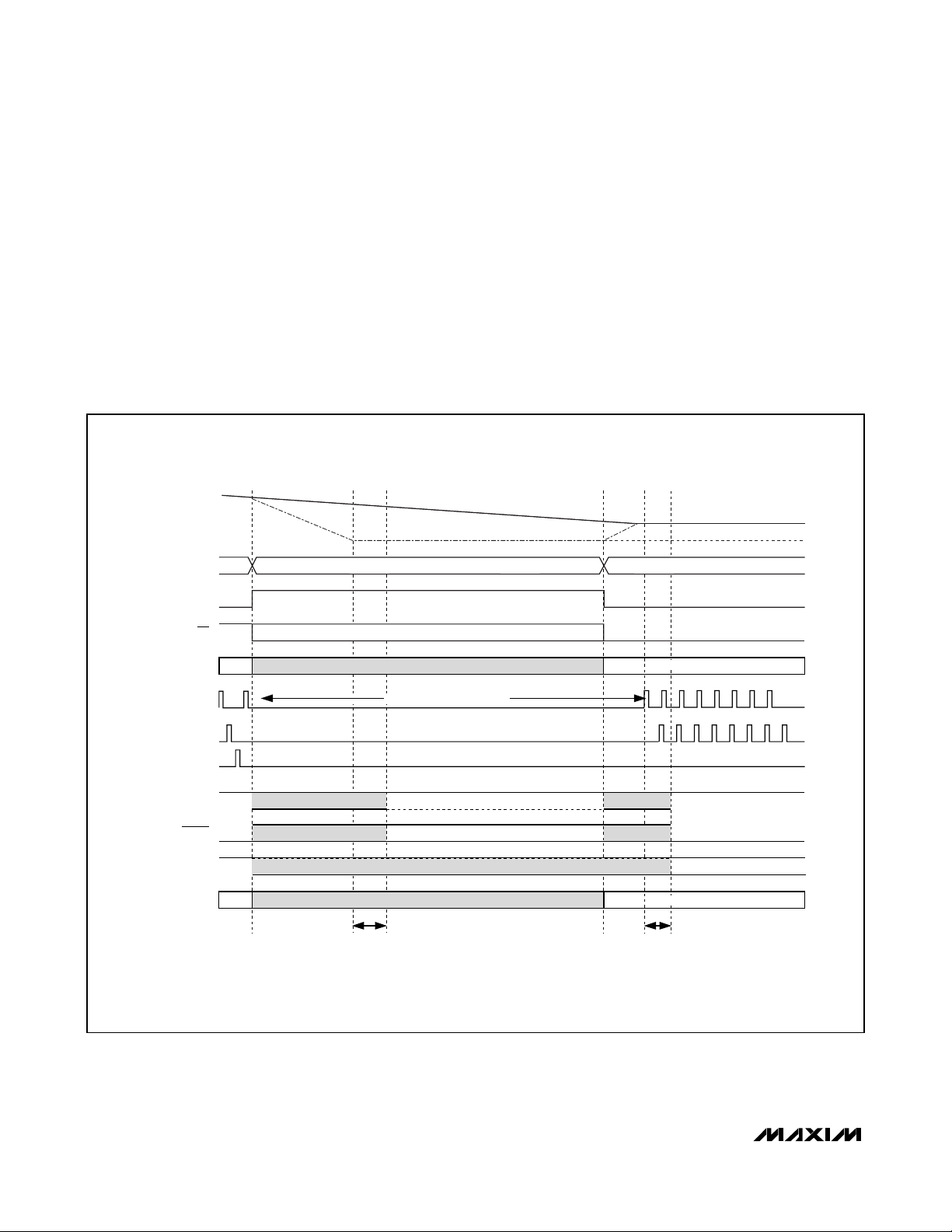
MAX8770/MAX8771/MAX8772
MAX8770/MAX8771/MAX8772 Dual-Phase, Quick-
PWM Controller for IMVP-6+ CPU Core Power Supplies
30 ______________________________________________________________________________________
CONFIDENTIAL INFORMATION – RESTRICTED TO INTEL®IMVP-6 LICENSEES
• Standard C4 Deeper Sleep Exit: When exiting
deeper sleep (DPRSLPVR pulled low) while the output voltage is regulating to the deeper sleep voltage,
the MAX8770/MAX8771/MAX8772 immediately activate all enabled phases and ramp the output voltage
to the LFM DAC code provided by the processor at
the slew rate set by R
TIME
. The controller blanks
PWRGD, PHASEGD, and CLKEN (forced high
impedance) until 20µs after the transition is completed. See Figure 5.
• Slow C4 Deeper Sleep Exit: When exiting deeper
sleep (DPRSLPVR high, DPRSTP pulled high) while
the output voltage is regulating to the deeper sleep
voltage, the MAX8770/MAX8771/MAX8772 remain in
1-phase skip mode and ramp the output voltage to the
LFM DAC code provided by the processor at 1/4 the
slew-rate set by R
TIME
. The controller blanks PWRGD,
PHASEGD, and CLKEN (forced high impedance) until
20µs after the transition is completed. See Figure 6.
Figure 4. C4E (C4 Early Exit) Transition
ACTUAL V
CPU CORE
VOLTAGE
VID (D0–D6)
DPRSLPVR
PSI
INTERNAL
PWM CONTROL
DO NOT CARE (DPRSLPVR DOMINATES STATE)
1-PHASE SKIP (DH1 ACTIVE, DH2 = DL2 = FORCED LOW)
INTERNAL TARGET
DEEPER SLEEP VID
OUT
FORCED PWM
t
BLANK
20µs TYP
NO PULSES: V
SET TO 1.75V MIN
DH1
PWM2
DH2
PWRGD
CLKEN
PHASEGD
OVP
BLANK HIGH-Z BLANK HIGH-ZBLANK HIGH THRESHOLD ONLY
BLANK LO
> V
OUT
TARGET
BLANK HIGH THRESHOLD ONLY
BLANK HIGH-Z
BLANK LO
TRACKS INTERNAL TARGET
t
BLANK
20µs TYP
Page 31
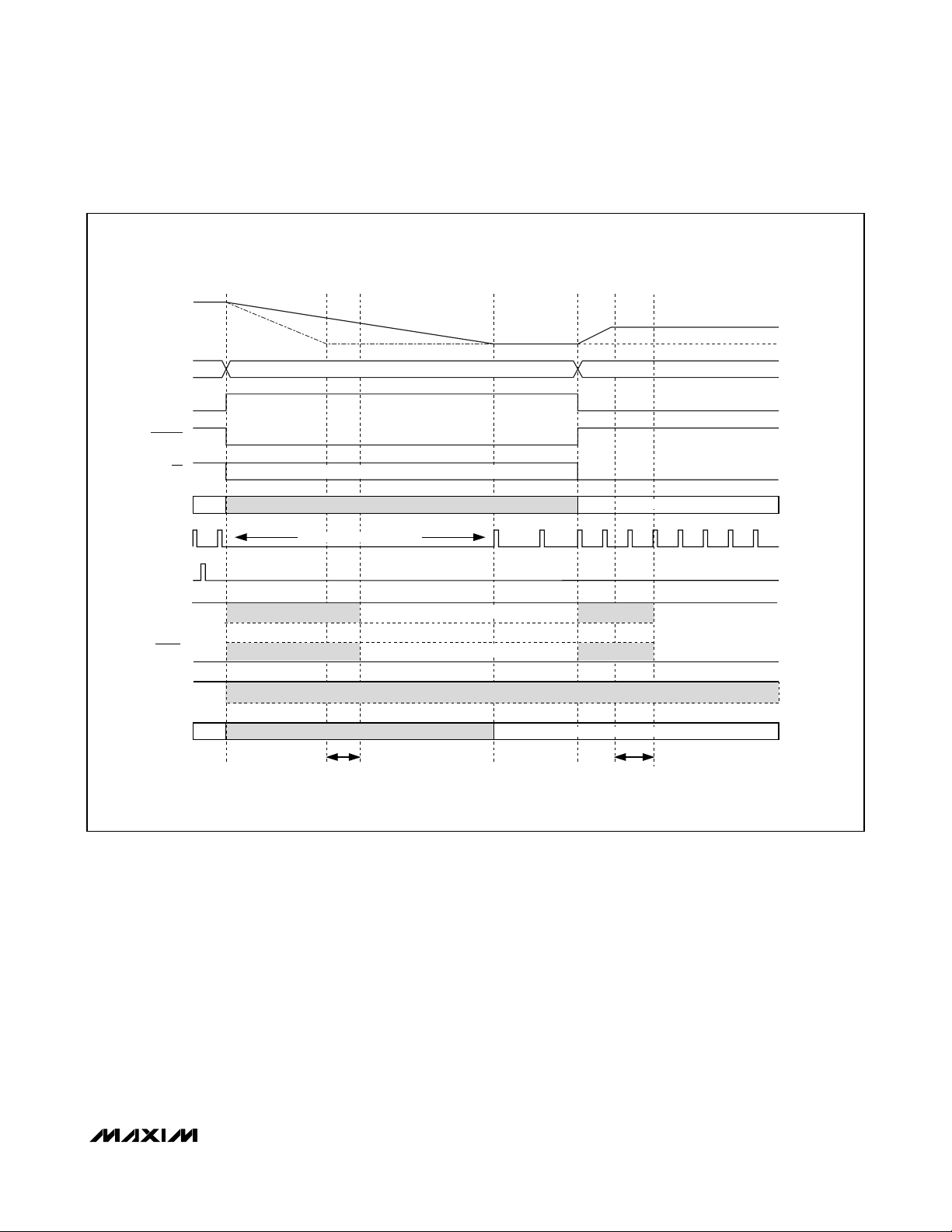
MAX8770/MAX8771/MAX8772
MAX8770/MAX8771/MAX8772 Dual-Phase, Quick-
PWM Controller for IMVP-6+ CPU Core Power Supplies
______________________________________________________________________________________ 31
CONFIDENTIAL INFORMATION – RESTRICTED TO INTEL®IMVP-6 LICENSEES
Figure 5. Standard C4 Transition
ACTIVE VID
CPU CORE
VOLTAGE
VID (D0–D6)
DPRSLPVR
DPRSTP
INTERNAL
TARGET
ACTUAL V
DEEPER SLEEP VID
OUT
LFM VID
DPRSLP VID
LFM VID
PSI
INTERNAL
PWM CONTROL
DH1
DH2
PWRGD
CLKEN
PHASEGD
OVP
DO NOT CARE (DPRSLPVR DOMINATES STATE)
1-PHASE SKIP (DH1 ACTIVE, DL2 FORCED LOW)
NO PULSES: V
BLANK HIGH-Z
BLANK LOW
SET TO 1.75V MIN TRACKS INTERNAL TARGET
20µs TYP
t
BLANK
> V
OUT
TARGET
BLANK HIGH THRESHOLD ONLY
BLANK HIGH THRESHOLD ONLY
BLANK HIGH-Z (1-PHASE OPERATION)
1-PHASE FORCED PWM
BLANK HIGH-Z
BLANK LOW
t
BLANK
20µs TYP
Page 32
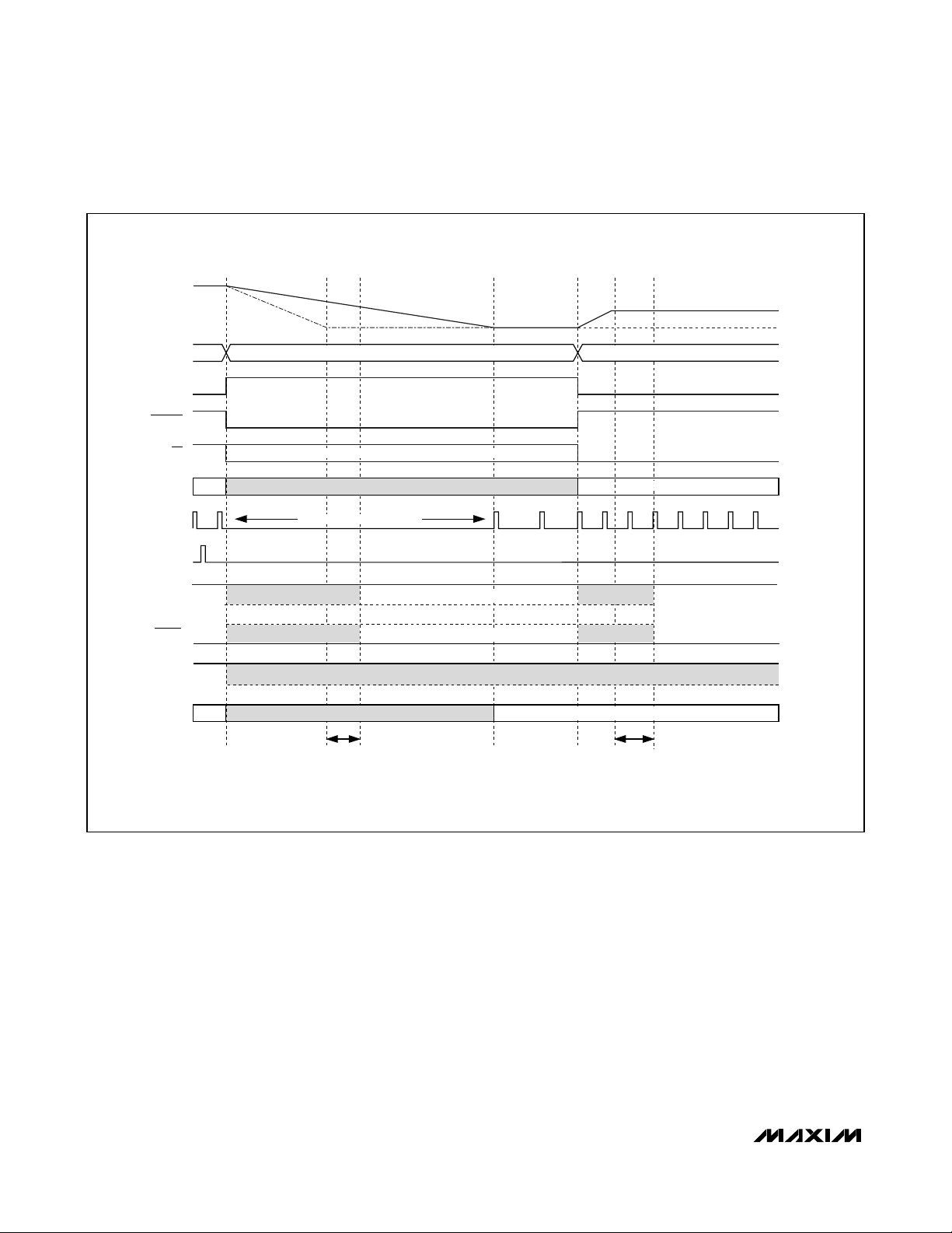
MAX8770/MAX8771/MAX8772
MAX8770/MAX8771/MAX8772 Dual-Phase, Quick-
PWM Controller for IMVP-6+ CPU Core Power Supplies
32 ______________________________________________________________________________________
CONFIDENTIAL INFORMATION – RESTRICTED TO INTEL®IMVP-6 LICENSEES
Figure 6. Slow C4 Transition
ACTIVE VID
CPU CORE
VOLTAGE
VID (D0–D6)
DPRSLPVR
DPRSTP
INTERNAL
TARGET
ACTUAL V
DEEPER SLEEP VID
OUT
LFM VID
DPRSLP VID
LFM VID
PSI
INTERNAL
PWM CONTROL
DH1
DH2
PWRGD
CLKEN
PHASEGD
BLANK HIGH-Z
BLANK LOW
DO NOT CARE (DPRSLPVR DOMINATES STATE)
1-PHASE SKIP (DH1 ACTIVE, DL2 FORCED LOW)
NO PULSES: V
> V
OUT
TARGET
BLANK HIGH THRESHOLD ONLY
BLANK HIGH THRESHOLD ONLY
BLANK HIGH-Z (1-PHASE OPERATION)
OVP
SET TO 1.75V MIN TRACKS INTERNAL TARGET
t
BLANK
20µs TYP
1-PHASE FORCED PWM
BLANK HIGH-Z
BLANK LOW
t
BLANK
20µs TYP
Page 33
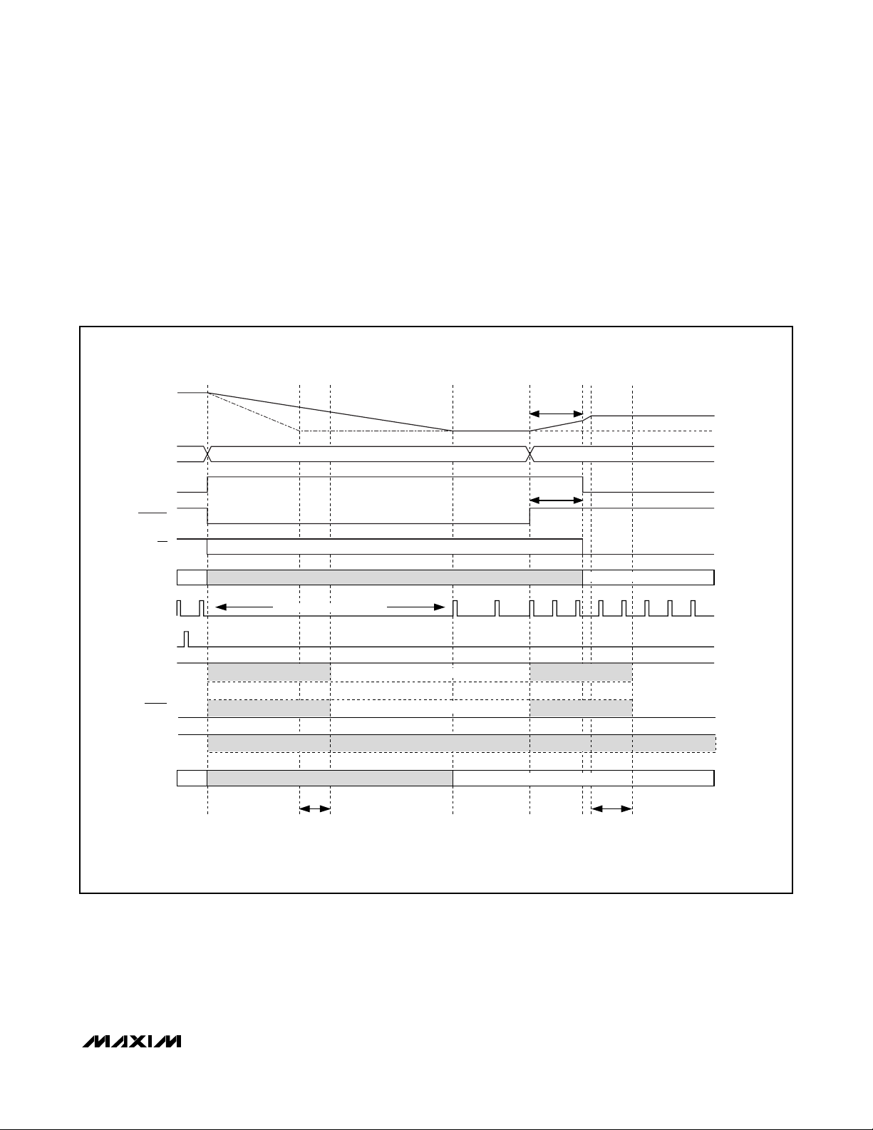
MAX8770/MAX8771/MAX8772
MAX8770/MAX8771/MAX8772 Dual-Phase, Quick-
PWM Controller for IMVP-6+ CPU Core Power Supplies
______________________________________________________________________________________ 33
CONFIDENTIAL INFORMATION – RESTRICTED TO INTEL®IMVP-6 LICENSEES
PSI
Transitions
When PSI is pulled low, the MAX8770/MAX8771/
MAX8772 immediately disable phase 2 (DH2 and DL2
forced low), blank PHASEGD high impedance, and enter
single-phase PWM operation (see Figure 7). When PSI is
pulled high, the MAX8770/MAX8771/MAX8772 enable
phase 2. PHASEGD is blanked high impedance for 32
switching cycles on DH2, allowing sufficient time/cycles
for phase 1 and 2 to achieve current balance. In a typical
IMVP-6 application, the VID is reduced by 1 LSB
(12.5mV) when PSI is pulled low, and increased by 1
LSB when PSI is pulled high.
Figure 7. PSI# Transition
ACTIVE VID
CPU CORE
VOLTAGE
VID (D0–D6)
DPRSLPVR
DPRSTP
PSI
INTERNAL
PWM CONTROL
DH1
INTERNAL
TARGET
DO NOT CARE (DPRSLPVR DOMINATES STATE)
1-PHASE SKIP (DH1 ACTIVE, DH2 = DL2 - FORCED LOW)
NO PULSES: V
ACTUAL V
DEEPER SLEEP VID
> V
OUT
TARGET
OUT
SLOW SLEW RATE
LFM VID
DPRSLP VID
LFM VID
SLOW SLEW RATE
1-PHASE FORCED PWM
DH2
PWRGD
CLKEN
PHASEGD
OVP
BLANK HIGH-Z
BLANK LOW
BLANK HIGH THRESHOLD ONLY
BLANK HIGH THRESHOLD ONLY
BLANK HIGH-Z (1-PHASE OPERATION)
SET TO 1.75V MIN TRACKS INTERNAL TARGET
t
BLANK
20µs TYP
BLANK HIGH-Z
BLANK LOW
t
BLANK
20µs TYP
Page 34
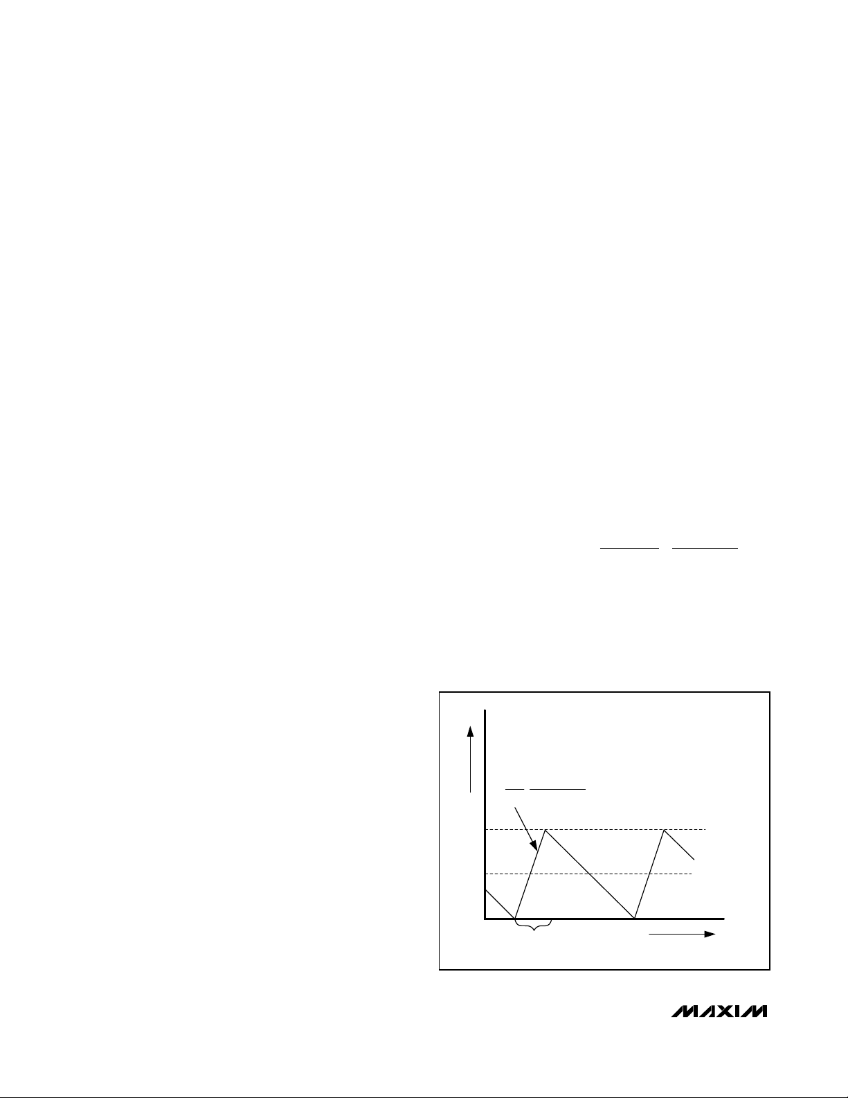
MAX8770/MAX8771/MAX8772
MAX8770/MAX8771/MAX8772 Dual-Phase, Quick-
PWM Controller for IMVP-6+ CPU Core Power Supplies
34 ______________________________________________________________________________________
CONFIDENTIAL INFORMATION – RESTRICTED TO INTEL®IMVP-6 LICENSEES
Forced-PWM Operation (Normal Mode)
During soft-start, soft-shutdown, and normal operation—when the CPU is actively running (DPRSLPVR =
low, Table 5)—the MAX8770/MAX8771/MAX8772 operate with the low-noise, forced-PWM control scheme.
Forced-PWM operation disables the zero-crossing
comparators of all active phases, forcing the low-side
gate-drive waveforms to be constantly the complement
of the high-side gate-drive waveforms. This keeps the
switching frequency constant and allows the inductor
current to reverse under light loads, providing fast,
accurate negative-output-voltage transitions by quickly
discharging the output capacitors.
Forced-PWM operation comes at a cost; the no-load
+5V bias supply current remains between 10mA to
50mA per phase, depending on the external MOSFETs
and switching frequency. To maintain high efficiency
under light-load conditions, the processor may switch
the controller to a low-power, pulse-skipping control
scheme after entering suspend mode.
PSI determines how many phases are active when
operating in forced-PWM mode (DPRSLPVR = low).
When PSI is pulled low, the main phase remains active
but the secondary phase is disabled (DH2 and DL2
forced low).
Light-Load Pulse-Skipping Operation
(Deeper Sleep)
When DPRSLPVR is pulled high, the MAX8770/
MAX8771/MAX8772 operate with a single-phase,
pulse-skipping mode. The pulse-skipping mode
enables the driver’s zero-crossing comparator, so the
controller pulls DL1 low when its current-sense inputs
detect “zero” inductor current. This keeps the inductor
from discharging the output capacitors and forces the
controller to skip pulses under light-load conditions to
avoid overcharging the output.
When pulse skipping, the controller blanks the upper
PWRGD and CLKEN thresholds, and also blanks
PHASEGD high impedance for the MAX8771. Upon
entering pulse-skipping operation, the controller temporarily sets the OVP threshold to 1.80V, preventing
false OVP faults when the transition to pulse-skipping
operation coincides with a downward VID code
change. Once the error amplifier detects that the output
voltage is in regulation, the OVP threshold tracks the
selected VID DAC code. The MAX8770/MAX8771/
MAX8772 automatically use forced-PWM operation during soft-start and soft-shutdown, regardless of the
DPRSLPVR and PSI configuration.
Automatic Pulse-Skipping Switchover
In skip mode (DPRSLPVR = high), an inherent automatic switchover to PFM takes place at light loads (Figure
8). This switchover is affected by a comparator that
truncates the low-side switch on-time at the inductor
current’s zero crossing. The zero-crossing comparator
senses the inductor current across the low-side
MOSFETs. Once V
LX
drops below the zero crossing
comparator threshold (see the Electrical Characteristics
table), the comparator forces DL low (Figure 2). This
mechanism causes the threshold between pulse-skipping PFM and nonskipping PWM operation to coincide
with the boundary between continuous and discontinuous inductor-current operation. The PFM/PWM
crossover occurs when the load current of each phase
is equal to 1/2 the peak-to-peak ripple current, which is
a function of the inductor value (Figure 8). For a battery-input 7V to 20V range, this threshold is relatively
constant, with only a minor dependence on the input
voltage due to the typically low duty cycles. The total
load current at the PFM/PWM crossover threshold
(I
LOAD(SKIP)
) is approximately:
where η
TOTAL
is the number of active phases.
The switching waveforms may appear noisy and asynchronous when light loading activates pulse-skipping
operation, but this is a normal operating condition that
results in high light-load efficiency. Trade-offs between
PFM noise and light-load efficiency are made by vary-
Figure 8. Pulse-Skipping/Discontinuous Crossover Point
I
=
LOAD SKIP TOTAL
()
INDUCTOR CURRENT
0
η
V
– V
BATT
OUT
L
∆i
∆t
ON-TIME
⎛
TVLVV
⎛
SW OUT IN OUT
⎜
⎝
TIME
−
⎞
⎟
⎜
⎠
V
⎝
IN
I
LOAD
I
PEAK
= I
PEAK
⎞
⎟
⎠
/2
Page 35
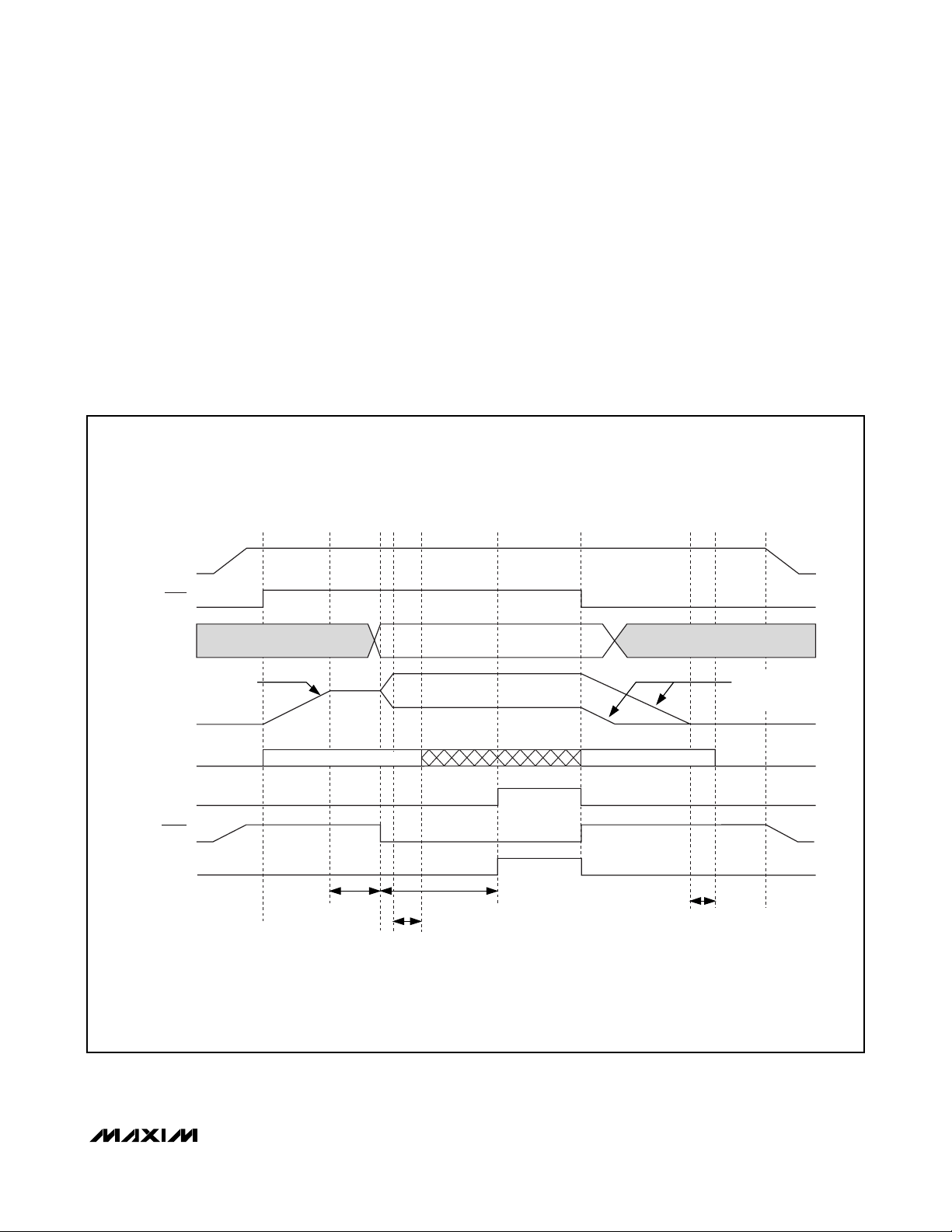
MAX8770/MAX8771/MAX8772
MAX8770/MAX8771/MAX8772 Dual-Phase, Quick-
PWM Controller for IMVP-6+ CPU Core Power Supplies
______________________________________________________________________________________ 35
CONFIDENTIAL INFORMATION – RESTRICTED TO INTEL®IMVP-6 LICENSEES
ing the inductor value. Generally, low inductor values
produce a broader efficiency vs. load curve, while
higher values result in higher full-load efficiency
(assuming that the coil resistance remains fixed) and
less output-voltage ripple. Penalties for using higher
inductor values include larger physical size and
degraded load-transient response, especially at low
input-voltage levels.
Power-Up Sequence (POR, UVLO)
The MAX8770/MAX8771/MAX8772 are enabled when
SHDN is driven high (Figure 9). The reference powers
up first. Once the reference exceeds its UVLO threshold, the internal analog blocks are turned on and
masked by a 150µs one-shot delay. The PWM controller then begins switching.
Power-on reset (POR) occurs when V
CC
rises above
approximately 2V, resetting the fault latch and preparing the controller for operation. The V
CC
UVLO circuitry
Figure 9. Power-Up and Shutdown Sequence Timing Diagram
V
CC
SHDN
VID (D0–D6)
INVALID
CODE
INVALID
CODE
SOFT-START =
1/8th SLEW RATE SET
V
CORE
INTERNAL
PWM CONTROL
PHASEGD
CLKEN
PWRGD
BY R
TIME
FORCED PWM
t
BLANK
60µs TYP
t
BLANK
20µs TYP
t
BLANK
5ms TYP
FORCED PWM
t
BLANK
20µs TYP
SOFT-SHUTDOWN =
1/8th SLEW RATE SET
BY R
TIME
Page 36

MAX8770/MAX8771/MAX8772
MAX8770/MAX8771/MAX8772 Dual-Phase, Quick-
PWM Controller for IMVP-6+ CPU Core Power Supplies
36 ______________________________________________________________________________________
CONFIDENTIAL INFORMATION – RESTRICTED TO INTEL®IMVP-6 LICENSEES
inhibits switching until VCCrises above 4.25V. The controller powers up the reference once the system
enables the controller, VCCabove 4.25V and SHDN dri-
ven high. With the reference in regulation, the controller
ramps the output voltage to the 1.20V boot voltage at
1/8 the slew rate set by R
TIME
:
where dV
TARGET
/dt = 12.5mV/µs x 71.5kΩ / R
TIME
is the
slew rate. The soft-start circuitry does not use a variable
current limit, so full output current is available immediately. CLKEN is pulled low approximately 60µs after the
MAX8770/MAX8771/MAX8772 reach the boot voltage. At
the same time, the MAX8770/MAX8771/MAX8772 slew
the output to the voltage set at the VID inputs at the programmed slew rate. PWRGD and PHASEGD become
high impedance approximately 5ms after CLKEN is
pulled low. The MAX8770/MAX8771/MAX8772 automatically use forced-PWM operation during soft-start and
soft-shutdown, regardless of the DPRSLPVR and PSI
configuration.
For automatic startup, the battery voltage should be
present before VCC. If the controller attempts to bring
the output into regulation without the battery-voltage
present, the fault latch trips. The controller remains shut
down until the fault latch is cleared by toggling SHDN
or cycling the VCCpower supply below 0.5V.
If the VCCvoltage drops below 4.25V, the controller
assumes that there is not enough supply voltage to
make valid decisions. To protect the output from overvoltage faults, the controller shuts down immediately
and forces a high-impedance output.
Shutdown
When SHDN goes low, the MAX8770/MAX8771/MAX8772
enter low-power shutdown mode. CLKEN is pulled high
and PWRGD is pulled low immediately, and the output
voltage ramps down at 1/8 the slew rate set by R
TIME
:
where dV
TARGET
/dt = 12.5mV/µs x 71.5kΩ / R
TIME
is
the slew rate. Slowly discharging the output capacitors
by slewing the output over a long period of time keeps
the average negative inductor current low (damped
response), thereby eliminating the negative output-voltage excursion that occurs when the controller discharges the output quickly by permanently turning on
the low-side MOSFET (underdamped response). This
eliminates the need for the Schottky diode normally
connected between the output and ground to clamp
the negative output-voltage excursion. After the controller reaches the zero target, the MAX8770/
MAX8771/MAX8772 shut down completely—the drivers
are disabled (DL1 and DL2 driven high)—the reference
turns off, and the supply currents drop to about 1µA
(max) 20µs.
When a fault condition—output UVLO or thermal shutdown—activates the shutdown sequence, the protection
circuitry sets the fault latch to prevent the controller from
restarting. To clear the fault latch and reactivate the controller, toggle SHDN or cycle V
CC
power below 0.5V.
Power Monitor (POUT)
The MAX8770/MAX8771/MAX8772 include a singlequadrant multiplier used to determine the actual output
power based on the inductor current (sum of the differential CS inputs) and output voltage (CSNpm to GNDS,
when CSNpm = CSN12 for MAX8771, CSNpm = CSN2
for MAX8770/MAX8772). The buffered output of this
multiplier is connected to POUT and provides a voltage
relative to the output power dissipation:
where the power-monitor scale factor (K
PWR
) is typically 16.67mV. The power monitor allows the system to
accurately monitor the CPU’s power dissipation and
quickly predict if the system is about to overheat before
the significantly slower temperature sensor signals an
overtemperature alert.
Phase Fault (PHASEGD, MAX8771 Only)
The MAX8771 includes a phase-fault output that signals the system that one of the two phases either has a
fault condition or is not matched with the other.
Detection is done by identifying the need for a large ontime difference between phases in order to achieve or
move towards current balance. PHASEGD is forced low
when V
CCI
is below 0.6xVFBor above 1.4xVFB.
PHASEGD is high impedance when the MAX8771 is set
to run in 1-phase operation (DPRSLPVR high, or PSI
low and DPRSLPVR low). On exit to the 2-phase mode,
PHASEGD is forced high impedance for 32 switching
cycles on DH2.
PHASEGD is low in shutdown. PHASEGD is forced high
impedance whenever the slew rate controller is active
(output voltage transitions).
t
TRAN START
()
8
V
=
BOOT
dV dt
()
TARGET
/
8
V
t
TRAN SHDN
()
=
OUT
dV dt
()
TARGET
/
VpmV I R
()()
V
=
PWR
−
CSN GNDS LOAD SENSE
K
PWR
Page 37

MAX8770/MAX8771/MAX8772
MAX8770/MAX8771/MAX8772 Dual-Phase, Quick-
PWM Controller for IMVP-6+ CPU Core Power Supplies
______________________________________________________________________________________ 37
CONFIDENTIAL INFORMATION – RESTRICTED TO INTEL®IMVP-6 LICENSEES
Temperature Comparator (
VRHOT
)
The MAX8770/MAX8771/MAX8772 also feature an
independent comparator with an accurate threshold
(V
HOT
) that tracks the analog supply voltage (V
HOT
=
0.3V
CC
). This makes the thermal trip threshold indepen-
dent of the V
CC
supply voltage tolerance. Use a resis-
tor- and thermistor-divider between V
CC
and GND to
generate a voltage-regulator overtemperature monitor.
Place the thermistor as close to the MOSFETs and
inductors as possible.
Fault Protection (Latched)
Output Overvoltage Protection (MAX8770/
MAX8771 Only)
The OVP circuit is designed to protect the CPU against
a shorted high-side MOSFET by drawing high current
and blowing the battery fuse. The MAX8770/MAX8771
continuously monitor the output for an overvoltage fault.
The controller detects an OVP fault if the output voltage
exceeds the set VID DAC voltage by more than 300mV,
regardless of the operating state. During pulse-skipping operation (DPRSLPVR = high), the OVP threshold
is set at 1.8V once a downward VID transition occurs,
and reverts to track the VID DAC voltage when the output reaches the set VID code.
When the OVP circuit detects an overvoltage fault while
in multiphase mode (DPRSLPVR = low, PSI = high), the
MAX8770/MAX8771 immediately force DL1 and DL2
high and pull DH1 and DH2 low. This action turns on
the synchronous-rectifier MOSFETs with 100% duty
and, in turn, rapidly discharges the output filter capacitor and forces the output low. If the condition that
caused the overvoltage (such as a shorted high-side
MOSFET) persists, the battery fuse blows. Toggle
SHDN or cycle the VCCpower supply below 0.5V to
clear the fault latch and reactivate the controller.
When an overvoltage fault occurs while in 1-phase
operation (DPRSLPVR = high, or PSI = low), the
MAX8770/MAX8771 immediately force DL1 high and
pull DH1 low. DL2 and DH2 remain low as phase 2 was
disabled. DL2 is forced high only when the output falls
below the UV threshold. Overvoltage protection can be
disabled through the no-fault test mode (see the No-
Fault Test Mode section).
Output Undervoltage Protection
The output UVP function is similar to foldback current
limiting, but employs a timer rather than a variable current limit. If the MAX8770/MAX8771/MAX8772 output
voltage is 400mV below the target voltage, the controller activates the shutdown sequence and sets the
fault latch. Once the controller ramps down to zero, it
forces the DL1 and DL2 high and pulls DH1 and DH2
low. Toggle SHDN or cycle the V
CC
power supply
below 0.5V to clear the fault latch and reactivate the
controller.
UVP can be disabled through the no-fault test mode
(see the No-Fault Test Mode section).
Thermal-Fault Protection
The MAX8770/MAX8771/MAX8772 feature a thermalfault-protection circuit. When the junction temperature
rises above +160°C, a thermal sensor sets the fault
latch and activates the soft-shutdown sequence. Once
the controller ramps down to zero, it forces the DL1 and
DL2 high and pulls DH1 and DH2 low. Toggle SHDN or
cycle the VCCpower supply below 0.5V to clear the
fault latch and reactivate the controller after the junction
temperature cools by 15°C.
Thermal shutdown can be disabled through the no-fault
test mode (see the No-Fault Test Mode section).
No-Fault Test Mode
The latched fault-protection features can complicate
the process of debugging prototype breadboards
since there are (at most) a few milliseconds in which to
determine what went wrong. Therefore, a “no-fault” test
mode is provided to disable the fault protection—overvoltage protection, undervoltage protection, and thermal shutdown. Additionally, the test mode clears the
fault latch if it has been set. The no-fault test mode is
entered by forcing 11V to 13V on SHDN.
MOSFET Gate Drivers
The DH and DL drivers are optimized for driving moderate-sized high-side and larger low-side power
MOSFETs. This is consistent with the low duty factor
seen in notebook applications where a large VIN- V
OUT
differential exists. The high-side gate drivers (DH)
source and sink 2.2A, and the low-side gate drivers
(DL) source 2.7A and sink 8A. This ensures robust gate
drive for high-current applications. The DH_ floating
high-side MOSFET drivers are powered by internal
boost switch charge pumps at BST_, while the DL_ synchronous-rectifier drivers are powered directly by the
5V bias supply (VDD).
Adaptive dead-time circuits monitor the DL and DH drivers and prevent either FET from turning on until the
other is fully off. The adaptive driver dead time allows
operation without shoot-through with a wide range of
MOSFETs, minimizing delays and maintaining efficiency.
There must be a low-resistance, low-inductance path
from the DL and DH drivers to the MOSFET gates for
the adaptive dead-time circuits to work properly; otherwise, the sense circuitry in the MAX8770/
Page 38
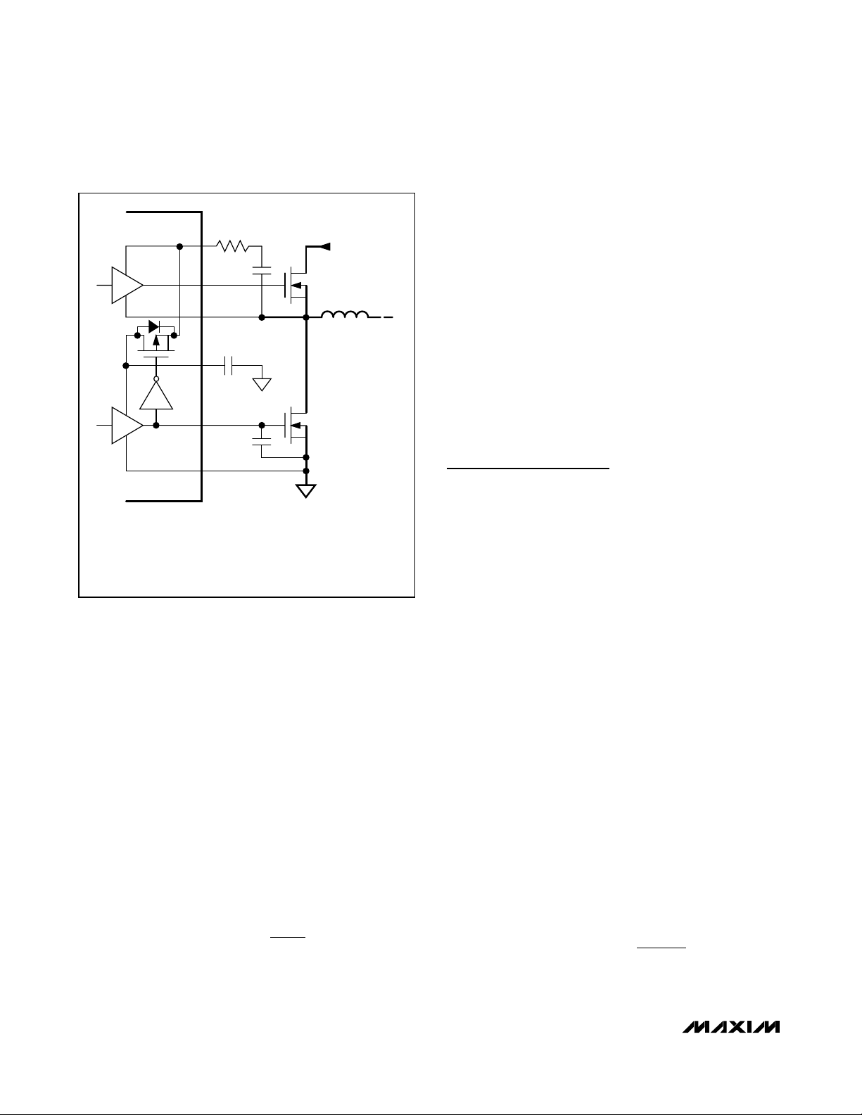
MAX8770/MAX8771/MAX8772
MAX8770/MAX8771/MAX8772 Dual-Phase, Quick-
PWM Controller for IMVP-6+ CPU Core Power Supplies
38 ______________________________________________________________________________________
CONFIDENTIAL INFORMATION – RESTRICTED TO INTEL®IMVP-6 LICENSEES
MAX8771/MAX8772 interprets the MOSFET gates as
“off” while charge actually remains. Use very short,
wide traces (50 mils to 100 mils wide if the MOSFET is
1in from the driver).
The internal pulldown transistor that drives DL low is
robust, with a 0.25Ω (typ) on-resistance. This helps prevent DL from being pulled up due to capacitive coupling from the drain to the gate of the low-side
MOSFETs when the inductor node (LX) quickly switches from ground to VIN. Applications with high-input voltages and long inductive driver traces may require
rising LX edges that do not pull up the low-side
MOSFETs’ gate, causing shoot-through currents. The
capacitive coupling between LX and DL created by the
MOSFET’s gate-to-drain capacitance (C
RSS
), gate-to-
source capacitance (C
ISS
- C
RSS
), and additional
board parasitics should not exceed the following minimum threshold:
Typically, adding a 4700pF between DL and power
ground (CNLin Figure 10), close to the low-side
MOSFETs, greatly reduces coupling. Do not exceed
22nF of total gate capacitance to prevent excessive
turn-off delays.
Alternatively, shoot-through currents may be caused by
a combination of fast high-side MOSFETs and slow lowside MOSFETs. If the turn-off delay time of the low-side
MOSFET is too long, the high-side MOSFETs can turn
on before the low-side MOSFETs have actually turned
off. Adding a resistor less than 5Ω in series with BST
slows down the high-side MOSFET turn-on time, eliminating the shoot-through currents without degrading
the turn-off time (R
BST
in Figure 10). Slowing down the
high-side MOSFET also reduces the LX node rise time,
thereby reducing EMI and high-frequency coupling
responsible for switching noise.
Multiphase Quick-PWM
Design Procedure
Firmly establish the input voltage range and maximum
load current before choosing a switching frequency
and inductor operating point (ripple-current ratio). The
primary design trade-off lies in choosing a good switching frequency and inductor operating point, and the following four factors dictate the rest of the design:
• Input voltage range: The maximum value (V
IN(MAX)
)
must accommodate the worst-case high-AC adapter
voltage. The minimum value (V
IN(MIN)
) must account
for the lowest input voltage after drops due to connectors, fuses, and battery selector switches. If there
is a choice at all, lower input voltages result in better
efficiency.
• Maximum load current: There are two values to
consider. The peak load current (I
LOAD(MAX)
) determines the instantaneous component stresses and filtering requirements, and thus drives output capacitor
selection, inductor saturation rating, and the design
of the current-limit circuit. The continuous load current (I
LOAD
) determines the thermal stresses and
thus drives the selection of input capacitors,
MOSFETs, and other critical heat-contributing components. Modern notebook CPUs generally exhibit
I
LOAD
= I
LOAD(MAX)
x 80%.
For multiphase systems, each phase supports a fraction of the load, depending on the current balancing.
When properly balanced, the load current is evenly distributed among each phase:
where η
TOTAL
is the total number of active phases.
Figure 10. Gate Drive Circuit
(R
)*
C
BYP
BST
C
BST
(CNL)*
INPUT (V
)
IN
N
H
L
N
L
BST
DH
LX
V
DD
DL
PGND
)* OPTIONAL—THE RESISTOR LOWERS EMI BY DECREASING THE
(R
BST
SWITCHING NODE RISE TIME.
)* OPTIONAL—THE CAPACITOR REDUCES LX TO DL CAPACITIVE
(C
NL
COUPLING THAT CAN CAUSE SHOOT-THROUGH CURRENTS
VV
GS TH IN
()
⎛
>
⎜
⎝
C
C
RSS
ISS
⎞
⎟
⎠
I
I
LOAD PHASE
()
=
LOAD
η
TOTAL
Page 39

MAX8770/MAX8771/MAX8772
MAX8770/MAX8771/MAX8772 Dual-Phase, Quick-
PWM Controller for IMVP-6+ CPU Core Power Supplies
______________________________________________________________________________________ 39
CONFIDENTIAL INFORMATION – RESTRICTED TO INTEL®IMVP-6 LICENSEES
• Switching frequency: This choice determines the
basic trade-off between size and efficiency. The optimal frequency is largely a function of maximum input
voltage due to MOSFET switching losses that are
proportional to frequency and V
IN
2
. The optimum frequency is also a moving target, due to rapid
improvements in MOSFET technology that are making higher frequencies more practical.
• Inductor operating point: This choice provides
trade-offs between size vs. efficiency and transient
response vs. output noise. Low inductor values provide better transient response and smaller physical
size, but also result in lower efficiency and higher
output noise due to increased ripple current. The
minimum practical inductor value is one that causes
the circuit to operate at the edge of critical conduction (where the inductor current just touches zero
with every cycle at maximum load). Inductor values
lower than this grant no further size-reduction benefit.
The optimum operating point is usually found
between 20% and 50% ripple current.
Inductor Selection
The switching frequency and operating point (% ripple
current or LIR) determine the inductor value as follows:
where η
TOTAL
is the total number of phases.
Find a low-loss inductor having the lowest possible DC
resistance that fits in the allotted dimensions. Ferrite
cores are often the best choice, although powdered
iron is inexpensive and can work well at 200kHz. The
core must be large enough not to saturate at the peak
inductor current (I
PEAK
):
Transient Response
The inductor ripple current impacts transient-response
performance, especially at low VIN- V
OUT
differentials.
Low inductor values allow the inductor current to slew
faster, replenishing charge removed from the output filter capacitors by a sudden load step. The amount of
output sag is also a function of the maximum duty factor, which can be calculated from the on-time and minimum off-time. For a dual-phase controller, the
worst-case output sag voltage may be determined by:
where t
OFF(MIN)
is the minimum off-time (see the
Electrical Characteristics table).
The amount of overshoot due to stored inductor energy
can be calculated as:
where η
TOTAL
is the total number of active phases.
Setting the Current Limit
The minimum current-limit threshold must be high
enough to support the maximum load current when the
current limit is at the minimum tolerance value. The valley of the inductor current occurs at I
LOAD(MAX)
minus
half the ripple current; therefore:
where η
TOTAL
is the total number of active phases,
and I
LIMIT(LOW)
equals the minimum current-limit
threshold voltage divided by the current-sense resistor
(R
SENSE
). For the 22.5mV default setting, the minimum
current-limit threshold is 19.5mV.
⎛
VV
−
L
=
η
TOTAL
IN OUT
⎜
f I LIRVV
⎝
SW LOAD MAX
()
⎞
⎛
⎞
OUT
⎟
⎜
⎟
⎝
IN
⎠
⎠
V
SAG
⎡
2
⎛
VT
∆
LI
()
LOAD(MAX)
=
CV
2
OUT OUT
∆
I
LOAD(MAX)
+
C
2
⎡
⎛
()
⎢
⎜
⎢
⎝
⎣
⎡
⎢⎢
OUT
⎢
⎣
OUT SW
⎢
⎜
⎝
⎢
⎣
VVT
2
−
IN OUT SW
V
IN
⎛
VT
OUT SW
⎜
V
⎝
IN
⎞
t
+
OFF MIN
⎟
V
⎠
IN
⎞
2
−
⎟
⎠
⎞
t
+
()
OFF MIN
⎟
⎠
()
t
()
OFF MIN
⎤
⎥
⎥
⎦
⎤
⎥
⎥
⎦
2
()
V
SOAR
IL
∆
()
≈
LOAD MAX
2η
CV
TOTAL OUT OUT
⎤
⎥
⎥
⎦
I
PEAK
I
⎛
LOAD MAX
=
⎜
η
⎝
TOTAL
⎞
()
⎟
⎠
LIR
⎛
1
⎜
⎝
⎞
+
⎟
⎠
2
I
LIMIT LOW
()
⎛
LOAD MAX
>
⎜
η
⎝
TOTAL
⎞
()
⎟
⎠
LIR
⎛
1
⎜
⎝
⎞
−
⎟
⎠
2
I
Page 40

MAX8770/MAX8771/MAX8772
MAX8770/MAX8771/MAX8772 Dual-Phase, Quick-
PWM Controller for IMVP-6+ CPU Core Power Supplies
40 ______________________________________________________________________________________
CONFIDENTIAL INFORMATION – RESTRICTED TO INTEL®IMVP-6 LICENSEES
Output Capacitor Selection
The output filter capacitor must have low enough ESR to
meet output ripple and load-transient requirements, yet
have high enough ESR to satisfy stability requirements.
In CPU V
CORE
converters and other applications where
the output is subject to large load transients, the output
capacitor’s size typically depends on how much ESR is
needed to prevent the output from dipping too low
under a load transient. Ignoring the sag due to finite
capacitance:
In non-CPU applications, the output capacitor’s size
often depends on how much ESR is needed to maintain
an acceptable level of output ripple voltage. The output
ripple voltage of a step-down controller equals the total
inductor ripple current multiplied by the output capacitor’s ESR. When operating multiphase systems out-ofphase, the peak inductor currents of each phase are
staggered, resulting in lower output ripple voltage by
reducing the total inductor ripple current. For multiphase operation, the maximum ESR to meet ripple
requirements is:
where η
TOTAL
is the total number of active phases and
fSWis the switching frequency per phase. The actual
capacitance value required relates to the physical size
needed to achieve low ESR, as well as to the chemistry
of the capacitor technology. Thus, the capacitor is usually selected by ESR and voltage rating rather than by
capacitance value (this is true of polymer types).
When using low-capacity ceramic filter capacitors,
capacitor size is usually determined by the capacity
needed to prevent V
SAG
and V
SOAR
from causing
problems during load transients. Generally, once
enough capacitance is added to meet the overshoot
requirement, undershoot at the rising load edge is no
longer a problem (see the V
SAG
and V
SOAR
equations
in the Transient Response section).
Output Capacitor Stability Considerations
For Quick-PWM controllers, stability is determined by
the value of the ESR zero relative to the switching
frequency. The boundary of instability is given by the
following equation:
where:
where C
OUT
is the total output capacitance, R
ESR
is the
total ESR, R
SENSE
is the current-sense resistance (R
CM
= RCS), R
DROOP
is the voltage-positioning gain, and
R
PCB
is the parasitic board resistance between the out-
put capacitors and sense resistors.
For a standard 300kHz application, the ESR zero frequency must be well below 95kHz, preferably below
50kHz. Tantalum, Sanyo POSCAP, and Panasonic SP
capacitors in widespread use at the time of publication
have typical ESR zero frequencies below 50kHz. In the
standard application circuit, the ESR needed to support
a 30mV
P-P
ripple is 30mV/(40A x 0.3) = 2.5mΩ. Four
330µF/2.5V Panasonic SP (type SX) capacitors in parallel provide 1.5mΩ (max) ESR. With a 2mΩ droop and
0.5mΩ PC board resistance, the typical combined ESR
results in a zero at 30kHz.
Ceramic capacitors have a high ESR zero frequency,
but applications with significant voltage positioning can
take advantage of their size and low ESR. Do not put
high-value ceramic capacitors directly across the output
without verifying that the circuit contains enough voltage
positioning and series PC board resistance to ensure
stability. When only using ceramic output capacitors,
output overshoot (V
SOAR
) typically determines the minimum output capacitance requirement. Their relatively
low capacitance value can cause output overshoot
when stepping from full-load to no-load conditions,
unless a small inductor value is used (high switching
frequency) to minimize the energy transferred from
inductor to capacitor during load-step recovery. The
efficiency penalty for operating at 600kHz is approximately 5% when compared to the 300kHz circuit, primarily due to the high-side MOSFET switching losses.
R
ESR
V
RR
()
≤
+
ESR PCB
⎡
⎢
VVV
η
−
()
⎢
IN TOTAL OUT OUT
⎣
Vf L
IN SW
≤
STEP
I
∆
LOAD MAX
()
⎤
V
⎥
RIPPLE
⎥
⎦
f
f
ESR
f
=
ESR
RRR R
EFF ESR DROOP PCB
2π
=+ +
SW
≤
π
1
RC
EFF OUT
and
Page 41

MAX8770/MAX8771/MAX8772
MAX8770/MAX8771/MAX8772 Dual-Phase, Quick-
PWM Controller for IMVP-6+ CPU Core Power Supplies
______________________________________________________________________________________ 41
CONFIDENTIAL INFORMATION – RESTRICTED TO INTEL®IMVP-6 LICENSEES
Unstable operation manifests itself in two related but
distinctly different ways: double-pulsing and feed-back
loop instability. Double pulsing occurs due to noise on
the output or because the ESR is so low that there is
not enough voltage ramp in the output voltage signal.
This “fools” the error comparator into triggering a new
cycle immediately after the minimum off-time period
has expired. Double pulsing is more annoying than
harmful, resulting in nothing worse than increased output ripple. However, it can indicate the possible presence of loop instability due to insufficient ESR. Loop
instability can result in oscillations at the output after
line or load steps. Such perturbations are usually
damped, but can cause the output voltage to rise
above or fall below the tolerance limits.
The easiest method for checking stability is to apply a
very fast zero-to-max load transient and carefully
observe the output voltage ripple envelope for overshoot and ringing. It can help to simultaneously monitor
the inductor current with an AC current probe. Do not
allow more than one cycle of ringing after the initial
step-response under/overshoot.
Input Capacitor Selection
The input capacitor must meet the ripple current
requirement (I
RMS
) imposed by the switching currents.
The multiphase Quick-PWM controllers operate out-ofphase while the Quick-PWM slave controllers provide
selectable out-of-phase or in-phase on-time triggering.
Out-of-phase operation reduces the RMS input current
by dividing the input current between several staggered stages. For duty cycles less than 100%/η
OUTPH
per phase, the I
RMS
requirements may be determined
by the following equation:
where η
TOTAL
is the total number of out-of-phase
switching regulators. The worst-case RMS current
requirement occurs when operating with VIN=
2η
TOTALVOUT
. At this point, the above equation simpli-
fies to I
RMS
= 0.5 x I
LOAD/ηTOTAL
.
For most applications, nontantalum chemistries (ceramic, aluminum, or OS-CON) are preferred due to their
resistance to inrush surge currents typical of systems
with a mechanical switch or connector in series with the
input. If the Quick-PWM controller is operated as the
second stage of a two-stage power-conversion system,
tantalum input capacitors are acceptable. In either configuration, choose an input capacitor that exhibits less
than +10°C temperature rise at the RMS input current
for optimal circuit longevity.
Power MOSFET Selection
Most of the following MOSFET guidelines focus on the
challenge of obtaining high load-current capability
when using high-voltage (>20V) AC adapters. Low-current applications usually require less attention.
The high-side MOSFET (NH) must be able to dissipate
the resistive losses plus the switching losses at both
V
IN(MIN)
and V
IN(MAX)
. Calculate both of these sums.
Ideally, the losses at V
IN(MIN)
should be roughly equal
to losses at V
IN(MAX)
, with lower losses in between. If
the losses at V
IN(MIN)
are significantly higher than the
losses at V
IN(MAX)
, consider increasing the size of N
H
(reducing R
DS(ON)
but with higher C
GATE
). Conversely,
if the losses at V
IN(MAX)
are significantly higher than the
losses at V
IN(MIN)
, consider reducing the size of N
H
(increasing R
DS(ON)
to lower C
GATE
). If VINdoes not
vary over a wide range, the minimum power dissipation
occurs where the resistive losses equal the switching
losses.
Choose a low-side MOSFET that has the lowest possible on-resistance (R
DS(ON)
), comes in a moderatesized package (i.e., one or two 8-pin SOs, DPAK, or
D2PAK), and is reasonably priced. Make sure that the
DL gate driver can supply sufficient current to support
the gate charge and the current injected into the parasitic gate-to-drain capacitor caused by the high-side
MOSFET turning on; otherwise, cross-conduction problems may occur (see the MOSFET Gate Driver section).
MOSFET Power Dissipation
Worst-case conduction losses occur at the duty factor
extremes. For the high-side MOSFET (NH), the worstcase power dissipation due to resistance occurs at the
minimum input voltage:
where η
TOTAL
is the total number of phases.
Generally, a small high-side MOSFET is desired to
reduce switching losses at high input voltages.
However, the R
DS(ON)
required to stay within package
power dissipation often limits how small the MOSFET
can be. Again, the optimum occurs when the switching
losses equal the conduction (R
DS(ON)
) losses. Highside switching losses do not usually become an issue
until the input is greater than approximately 15V.
Calculating the power dissipation the in high-side MOSFET (NH) due to switching losses is difficult since it
must allow for difficult quantifying factors that influence
the turn-on and turn-off times. These factors include the
internal gate resistance, gate charge, threshold volt-
I
RMS
=
⎛
I
LOAD
⎜
η
⎝
TOTAL IN
⎞
⎟
V
⎠
VV V
ηη
TOTAL OUT IN TOTAL OUT
−
()
⎛
⎞
OUT
V
IN
⎛
⎟
⎜
⎠
⎝
PD N sistive
( Re )
H
V
=
⎜
⎝
I
LOAD
η
TOTAL
2
⎞
R
()
DS ON
⎟
⎠
Page 42

MAX8770/MAX8771/MAX8772
MAX8770/MAX8771/MAX8772 Dual-Phase, Quick-
PWM Controller for IMVP-6+ CPU Core Power Supplies
42 ______________________________________________________________________________________
CONFIDENTIAL INFORMATION – RESTRICTED TO INTEL®IMVP-6 LICENSEES
age, source inductance, and PC board layout characteristics. The following switching-loss calculation provides only a very rough estimate and is no substitute for
breadboard evaluation, preferably including verification
using a thermocouple mounted on NH:
where C
OSS
is the NHMOSFET’s output capacitance,
Q
G(SW)
is the charge needed to turn on the NHMOS-
FET, and I
GATE
is the peak gate-drive source/sink cur-
rent (2.2A typ).
Switching losses in the high-side MOSFET can become
an insidious heat problem when maximum AC adapter
voltages are applied due to the squared term in the C x
V
IN
2
x ƒSWswitching-loss equation. If the high-side
MOSFET chosen for adequate R
DS(ON)
at low battery
voltages becomes extraordinarily hot when biased from
V
IN(MAX)
, consider choosing another MOSFET with
lower parasitic capacitance.
For the low-side MOSFET (NL), the worst-case power
dissipation always occurs at maximum input voltage:
The worst case for MOSFET power dissipation occurs
under heavy overloads that are greater than
I
LOAD(MAX)
, but are not quite high enough to exceed
the current limit and cause the fault latch to trip. To protect against this possibility, you can “overdesign” the
circuit to tolerate:
where I
VALLEY(MAX)
is the maximum valley current
allowed by the current-limit circuit, including threshold
tolerance and on-resistance variation. The MOSFETs
must have a good size heatsink to handle the overload
power dissipation.
Choose a Schottky diode (DL) with a forward voltage
low enough to prevent the low-side MOSFET body
diode from turning on during the dead time. Select a
diode that can handle the load current per phase during the dead times. This diode is optional and can be
removed if efficiency is not critical.
Boost Capacitors
The boost capacitors (C
BST
) must be selected large
enough to handle the gate-charging requirements of
the high-side MOSFETs. Typically, 0.1µF ceramic
capacitors work well for low-power applications driving
medium-sized MOSFETs. However, high-current applications driving large, high-side MOSFETs require boost
capacitors larger than 0.1µF. For these applications,
select the boost capacitors to avoid discharging the
capacitor more than 200mV while charging the high
side MOSFETs’ gates:
where N is the number of high side MOSFETs used for
one regulator, and Q
GATE
is the gate charge specified
in the MOSFET’s data sheet. For example, assume (2)
IRF7811W n-channel MOSFETs are used on the high
side. According to the manufacturer’s data sheet, a single IRF7811W has a maximum gate charge of 24nC
(VGS= 5V). Using the above equation, the required
boost capacitance would be:
Selecting the closest standard value, this example
requires a 0.22µF ceramic capacitor.
Current-Balance Compensation (CCI)
The current-balance compensation capacitor (C
CCI
)
integrates the difference between the main and secondary current-sense voltages. The internal compensation resistor (R
CCI
= 200kΩ) improves transient
response by increasing the phase margin. This allows
the dynamics of the current-balance loop to be optimized. Excessively large capacitor values increase the
integration time constant, resulting in larger current differences between the phases during transients.
Excessively small capacitor values allow the current
loop to respond cycle-by-cycle, but can result in small
DC current variations between the phases. Likewise,
excessively large resistor values can also cause DC
current variations between the phases. Small resistor
values reduce the phase margin, resulting in marginal
PD N SWITCHING
( )
H
VIf Q
⎛
IN MAX LOAD SW
() ()
⎜
η
⎝
TOTAL
⎞
⎛
GSW
⎟
⎜
I
⎠
⎝
GATE
=
⎞
CVf
OSS IN SW
+
⎟
⎠
2
2
PD N RESISTIVE
( )
V
OUT
()
L
⎤
⎞
⎛
I
LOAD
⎥
⎟
⎜
η
⎥
⎝
TOTAL
⎠
⎦
⎡
⎛
⎢
−
1
⎜
V
⎢
⎣
IN MAX
⎝
=
2
⎞
R
DS ON
⎟
⎠
()
C
BST
C
BST
NQ
=×
200
×=224
GATE
mV
200
nC
.=
mV
024µ
F
I
II
=+
LOAD TOTAL VALLEY MAX
η
=+
η
TOTAL VALLEY MAX
⎛
⎜
⎝
I
()
()
∆
INDUCTOR
I LIR
⎛
LOAD MAX
⎜
⎝
()
2
⎞
⎟
⎠
2
⎞
⎟
⎠
Page 43
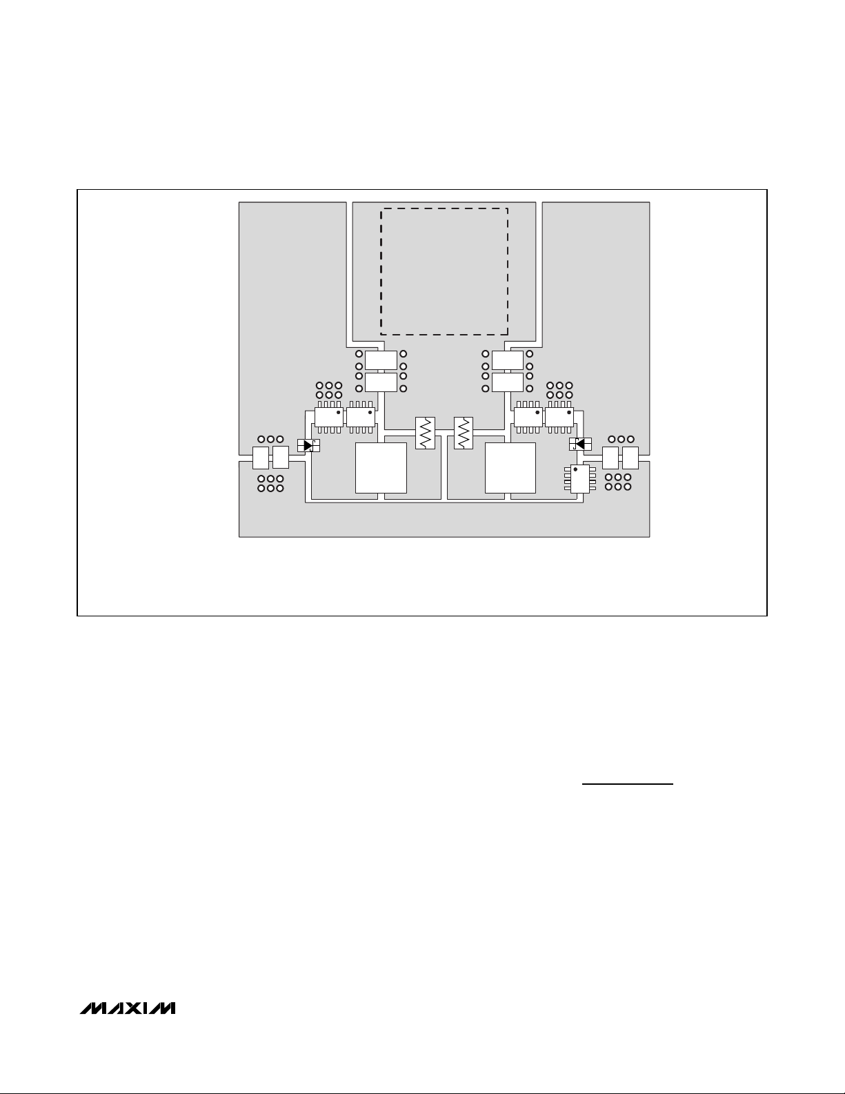
MAX8770/MAX8771/MAX8772
MAX8770/MAX8771/MAX8772 Dual-Phase, Quick-
PWM Controller for IMVP-6+ CPU Core Power Supplies
______________________________________________________________________________________ 43
CONFIDENTIAL INFORMATION – RESTRICTED TO INTEL®IMVP-6 LICENSEES
stability in the current-balance loop. For most applications, a 470pF capacitor from CCI to the switching regulator’s output works well.
Connecting the compensation network to the output
(V
OUT
) allows the controller to feed-forward the outputvoltage signal, especially during transients. To reduce
noise pickup in applications that have a widely distributed layout, it is sometimes helpful to connect the compensation network to the quiet analog ground rather
than V
OUT
.
Voltage Positioning and Loop
Compensation
Voltage positioning dynamically lowers the output voltage in response to the load current, reducing the output capacitance and processor’s power-dissipation
requirements. The controller uses a transconductance
amplifier to set the transient and DC output voltage
droop (Figure 2) as a function of the load. This adjustability allows flexibility in the selected current-sense
resistor value or inductor DCR, and allows smaller cur-
rent-sense resistance to be used, reducing the overall
power dissipated.
Steady-State Voltage Positioning
Connect a resistor (RFB) between FB and V
OUT
to set
the DC steady-state droop (load line) based on the
required voltage-positioning slope (R
DROOP
):
where the effective current-sense resistance (R
SENSE
)
depends on the current-sense method (see the Current
Sense section), and the voltage-positioning amplifier’s
transconductance (G
m(FB)
) is typically 600µS, as
defined in the Electrical Characteristics table. The controller sums together the input signals of the currentsense inputs (CSP_, CSN_).
When the inductors’ DCR is used as the current-sense
element (R
SENSE
= R
DCR
), each current-sense input
should include an NTC thermistor to minimize the temperature dependence of the voltage-positioning slope.
Figure 11. PC Board Layout Example
CPU
POWER
GROUND
C
C
OUT
OUT
C
C
OUT
OUT
IN
IN
IN
C
C
CINC
PLACE CONTROLLER ON BACKSIDE WHEN POSSIBLE, USING THE
GROUND PLANE TO SHIELD THE IC FROM EMI.
SEE THE EVALUATION KIT FOR ANALOG/POWER GROUND AND
CONTROLLER LAYOUT EXAMPLE.
INDUCTOR
INDUCTOR
POWER
GROUND
C
C
OUT
OUT
C
C
OUT
OUTPUT
INPUT
OUT
INDUCTOR
INDUCTOR
CINC
IN
R
R
=
FB
DROOP
RG
SENSE m FB
()
Page 44
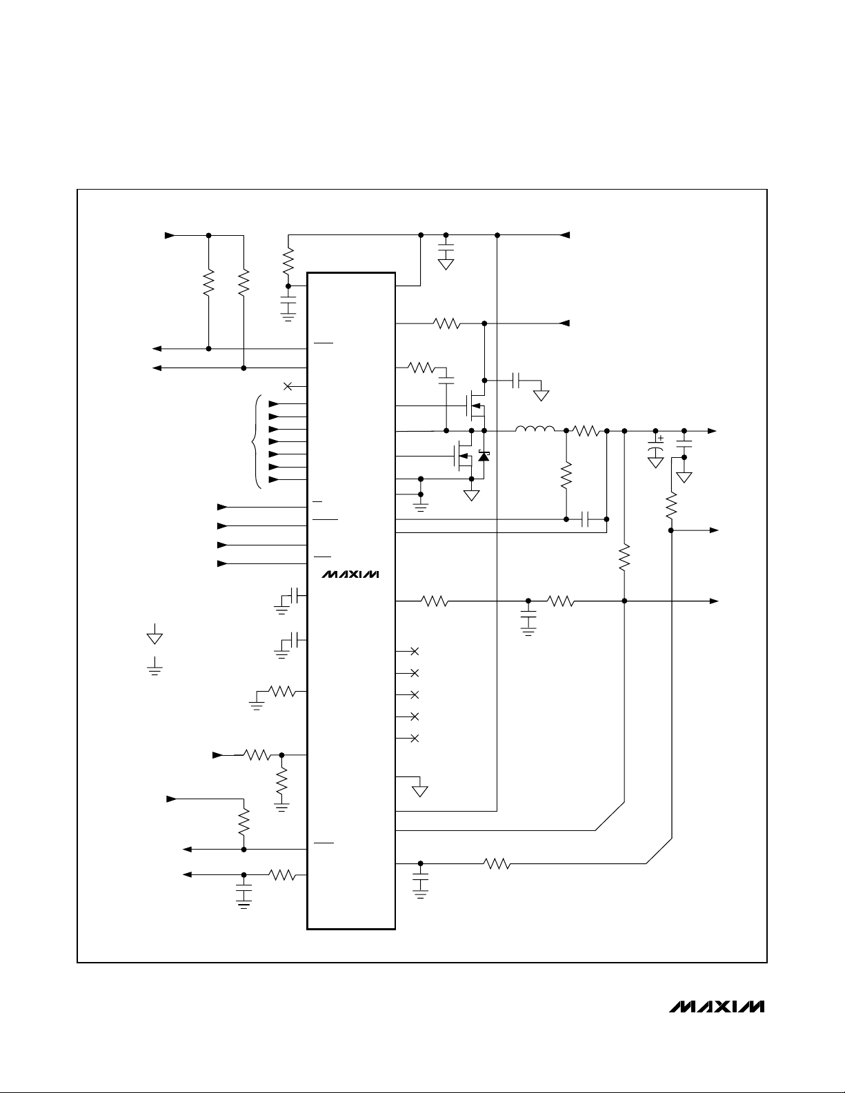
MAX8770/MAX8771/MAX8772
MAX8770/MAX8771/MAX8772 Dual-Phase, Quick-
PWM Controller for IMVP-6+ CPU Core Power Supplies
44 ______________________________________________________________________________________
CONFIDENTIAL INFORMATION – RESTRICTED TO INTEL®IMVP-6 LICENSEES
Figure 12. Single-Phase ULV Design
3.3V BIAS
SUPPLY
C1
R9
4.12kΩ
C9
4700pF
R18
200kΩ
N
L1
2.2µF
C3
0.22µF
N
H1
R1
R3
1.9kΩR21.9kΩ
CLK_ENABLE#
IMVPOK
DAC INPUTS
(1V LOGIC)
PSI#
DPRSTP#
DPRLSPVR
VR_ON
POWER GROUND
ANALOG GROUND
V
CC
1.2V BIAS
SUPPLY
56Ω
C10
0.1µF
10Ω
V
CC
CLKEN
PWRGD
PHASEGD
D0
D1
D2
D3
D4
D5
D6
PSI
DPRSTP
DPRSLPVR
SHDN
MAX8770
CCV
MAX8771
2.2µF
1000pF
C2
C5
MAX8772
C6
0.1µF
71.5kΩ
R6
13kΩ
NTC4
100kΩ
R7
R5
R8
10kΩ
REF
TIME
THRM
VRHOT
POUT
V
DD
RTON
R22
BST1
+
PGND1
CSP1
*CSN1
BST2
PGND2
CSP2
*CSN2
GNDS
0Ω
DH1
LX1
DL1
GND
FB
CCI
DH2
LX2
DL2
C
IN
R17
100
Ω
*
CSN1 AND CSN2 ARE BONDED TOGETHER ON THE
MAX8771 AND CALLED CSN12.
**
OPTIONAL -- RESISTOR ALLOW REMOTE SENSING FOR SYSTEM
VERIFICATION WHEN THE CPU IS NOT PRESENT;
PHASEGD IS ONLY ON THE MAX8771.
L1
R12
100Ω
C8
4700pF
R10
100Ω
5V BIAS
SUPPLY
INPUT V
8V TO 24V
RCS1
2mΩ
C11
2.2nF
IN
R11*
10Ω
OUTPUT
C
OUT
R16*
10Ω
CPU GND
SENSE
CPU V
CC
SENSE
Page 45

MAX8770/MAX8771/MAX8772
MAX8770/MAX8771/MAX8772 Dual-Phase, Quick-
PWM Controller for IMVP-6+ CPU Core Power Supplies
______________________________________________________________________________________ 45
CONFIDENTIAL INFORMATION – RESTRICTED TO INTEL®IMVP-6 LICENSEES
Minimum Input-Voltage Requirements and
Dropout Performance
The output voltage-adjustable range for continuousconduction operation is restricted by the nonadjustable
minimum off-time one-shot and the number of phases.
For best dropout performance, use the slower (200kHz)
on-time settings. When working with low input voltages,
the duty-factor limit must be calculated using worstcase values for on- and off-times.
Manufacturing tolerances and internal propagation
delays introduce an error to the on-times. This error is
greater at higher frequencies. Also, keep in mind that
transient response performance of buck regulators
operated too close to dropout is poor, and bulk output
capacitance must often be added (see the V
SAG
equa-
tion in the Design Procedure section).
The absolute point of dropout is when the inductor current ramps down during the minimum off-time (∆I
DOWN
)
as much as it ramps up during the on-time (∆I
UP
). The
ratio h = ∆I
UP
/∆I
DOWN
is an indicator of the ability to
slew the inductor current higher in response to
increased load, and must always be greater than 1. As
h approaches 1, the absolute minimum dropout point,
the inductor current cannot increase as much during
each switching cycle and V
SAG
greatly increases
unless additional output capacitance is used.
A reasonable minimum value for h is 1.5, but adjusting
this up or down allows tradeoffs between V
SAG
, output
capacitance, and minimum operating voltage. For a
given value of h, the minimum operating voltage can be
calculated as:
where V
DROOP
is the voltage-positioning droop, V
CHG
is the parasitic voltage drops in the charge path (see
the On-Time One-Shot section) and t
OFF(MIN)
is from
the Electrical Characteristics table. The absolute mini-
mum input voltage is calculated with h = 1.
If the calculated V
IN(MIN)
is greater than the required minimum input voltage, then reduce the operating frequency
or add output capacitance to obtain an acceptable V
SAG
.
If operation near dropout is anticipated, calculate V
SAG
to
be sure of adequate transient response.
Dropout design example:
V
VID
= 1.15V
f
SW
= 300kHz
t
OFF(MIN)
= 375ns
V
DROOP
= 2.1mV/A x 44A = 92.4mV
V
CHG
= 150mV (44A Load)
h = 1.5
Calculating again with h = 1 gives the absolute limit of
dropout:
Therefore, V
IN
must be greater than 4.1V, even with
very large output capacitance, and a practical input
voltage with reasonable output capacitance would be
5.0V.
Applications Information
PC Board Layout Guidelines
Careful PC board layout is critical to achieve low switching
losses and clean, stable operation. The switching power
stage requires particular attention (Figure 11). If possible,
mount all the power components on the top side of the
board with their ground terminals flush against one another. Follow these guidelines for good PC board layout:
1) Keep the high-current paths short, especially at the
ground terminals. This is essential for stable, jitter-free
operation.
2) Connect all analog grounds to a separate solid cop-
per plane, which connects to the GND pin of the
Quick-PWM controller. This includes the V
CC
bypass
capacitor, REF and GNDS bypass capacitors, and
compensation (CCV) components.
3) Keep the power traces and load connections short.
This is essential for high efficiency. The use of thick
copper PC boards (2oz vs. 1oz) can enhance fullload efficiency by 1% or more. Correctly routing PC
board traces is a difficult task that must be
approached in terms of fractions of centimeters,
where a single mΩ of excess trace resistance causes
a measurable efficiency penalty.
4) Keep the high-current, gate-driver traces (DL, DH,
LX, and BST) short and wide to minimize trace resistance and inductance. This is essential for high-
⎤
⎦
⎥
⎥
V
()
IN MIN
⎡
VV V
−+
VID DROOP CHG
=
⎢
1
ht f
−×
⎢
⎣
OFF MIN SW
()
V
V
IN MIN()
IN MIN()
⎡
⎢
⎣
⎡
⎢
⎣
VmVmV
. .
1 15 92 4 150
(. . )
−××
1 0 375 1 5 300
VmVmV
. .
1 15 92 4 150
(. . )
−××
1 0 375 1 0 300
−+
s kHz
µ
−+
s kHz
µ
⎤
⎥
⎦
⎤
⎥
⎦
.=
=
145
.=
=
136
V
V
Page 46
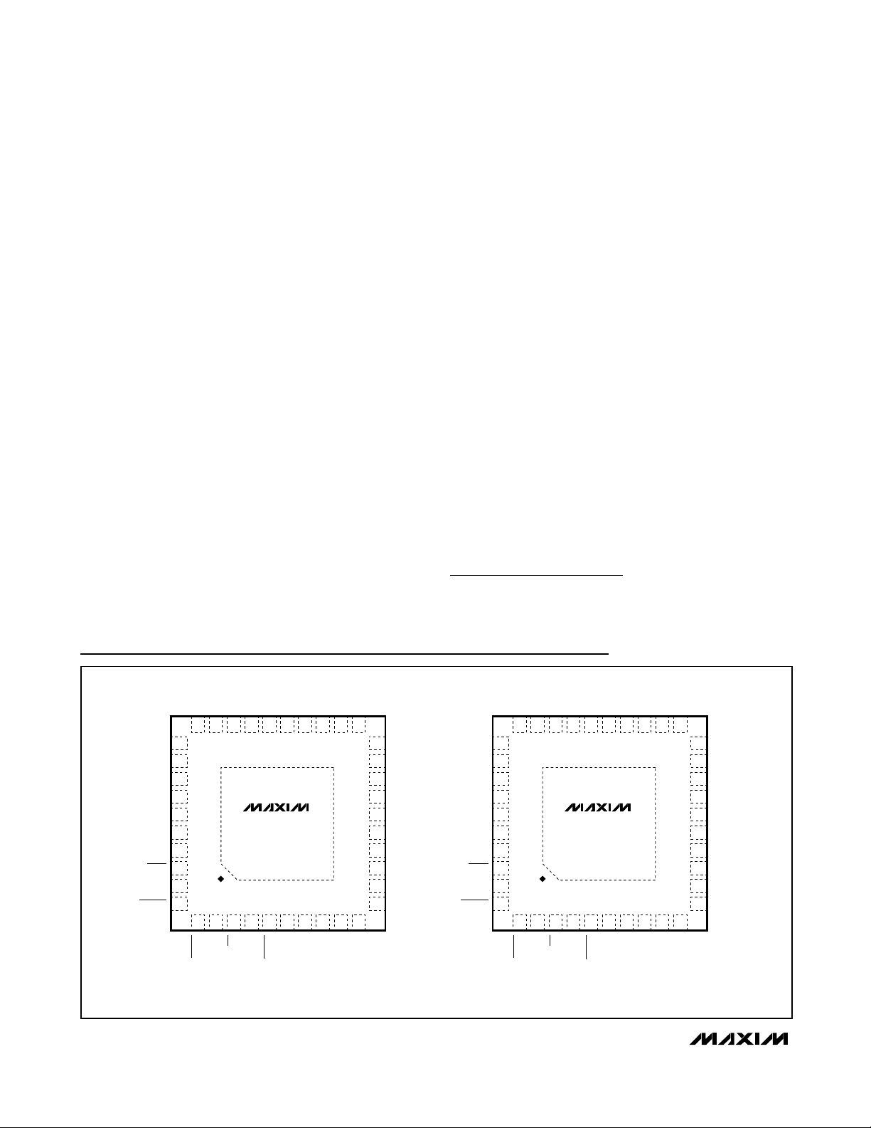
MAX8770/MAX8771/MAX8772
MAX8770/MAX8771/MAX8772 Dual-Phase, Quick-
PWM Controller for IMVP-6+ CPU Core Power Supplies
46 ______________________________________________________________________________________
CONFIDENTIAL INFORMATION – RESTRICTED TO INTEL®IMVP-6 LICENSEES
power MOSFETs that require low-impedance gate
drivers to avoid shoot-through currents.
5) CSP_ and CSN_ connections for current limiting and
voltage positioning must be made using Kelvin-sense
connections to guarantee the current-sense accuracy.
6) When trade-offs in trace lengths must be made, it is
preferable to allow the inductor charging path to be
made longer than the discharge path. For example, it
is better to allow some extra distance between the
input capacitors and the high-side MOSFET than to
allow distance between the inductor and the low-side
MOSFET or between the inductor and the output filter
capacitor.
7) Route high-speed switching nodes away from sensitive analog areas (REF, CCV, CCI, FB, CSP_, CSN_,
etc.).
Layout Procedure
Place the power components first, with ground terminals
adjacent (low-side MOSFET source, CIN, C
OUT
, and D1
anode). If possible, make all these connections on the top
layer with wide, copper-filled areas:
Mount the controller IC adjacent to the low-side MOSFET.
The DL gate traces must be short and wide (50 mils to 100
mils wide if the MOSFET is 1in from the controller IC).Group
the gate-drive components (BST capacitors, VDDbypass
capacitor) together near the controller IC.
Make the DC-DC controller ground connections as shown
in the Standard Application Circuits. This diagram can be
viewed as having four separate ground planes: input/output ground, where all the high-power components go; the
power ground plane, where the PGND pin and V
DD
bypass capacitor go; the master’s analog ground plane
where sensitive analog components, the master’s GND
pin, and V
CC
bypass capacitor go; and the slave’s analog
ground plane where the slave’s GND pin and VCCbypass
capacitor go. The master’s GND plane must meet the
PGND plane only at a single point directly beneath the IC.
Similarly, the slave’s GND plane must meet the PGND
plane only at a single point directly beneath the IC. The
respective master and slave ground planes should connect to the high-power output ground with a short metal
trace from PGND to the source of the low-side MOSFET
(the middle of the star ground). This point must also be
very close to the output capacitor ground terminal.
Connect the output power planes (V
CORE
and system
ground planes) directly to the output filter capacitor
positive and negative terminals with multiple vias. Place
the entire DC-DC converter circuit as close to the CPU
as is practical.
Chip Information
TRANSISTOR COUNT: 8990
PROCESS: BiCMOS
Pin Configurations
TOP VIEW
D0
D1
D2
D3
D4
D5
D6
SHDN
DPRSLPVR
DPRSTP
A "+" SIGN REPLACES THE FIRST PIN INDICATOR ON LEAD-FREE PACKAGES.
BST1
DH1
PGND1
LX1
27282930 26 24 23 22
31
32
33
34
35
36
37
38
39
40
12 4 56 7
CLKEN
3
PSI
PWRGD
6mm x 6mm
MAX8770
MAX8772
POUT
THIN QFN
DL1
25
VRHOT
VDDDL2
TIME
THRM
PGND2
LX2
21
8910
TON
CCV
DH2
CCI
20
BST2
19
V
CC
18
GND
17
CSP1
16
CSN1
15
CSN2
14
CSP2
13
GNDS
12
FB
11
REF
TOP VIEW
SHDN
DPRSLPVR
DPRSTP
BST1
DH1
31
D0
32
D1
33
D2
34
D3
35
D4
36
D5
37
D6
38
39
40
12 4 56 7
CLKEN
PWRGD
PGND1
DL1
LX1
27282930 26 24 23 22
VDDDL2
25
MAX8771
3
PSI
POUT
THRM
VRHOT
THIN QFN
6mm x 6mm
PGND2
8910
TON
TIME
LX2
CCV
DH2
21
20
BST2
19
V
CC
18
GND
17
PHASEGD
16
CSP1
15
CSN12
14
CSP2
13
GNDS
12
FB
11
REF
CCI
Page 47
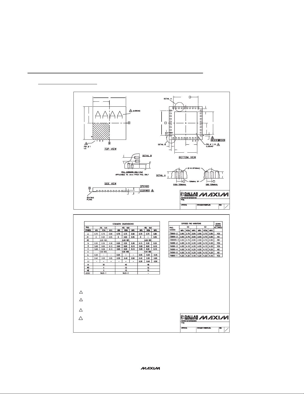
MAX8770/MAX8771/MAX8772
MAX8770/MAX8771/MAX8772 Dual-Phase, Quick-
PWM Controller for IMVP-6+ CPU Core Power Supplies
Maxim cannot assume responsibility for use of any circuitry other than circuitry entirely embodied in a Maxim product. No circuit patent licenses are
implied. Maxim reserves the right to change the circuitry and specifications without notice at any time.
Maxim Integrated Products, 120 San Gabriel Drive, Sunnyvale, CA 94086 408-737-7600 ____________________ 47
© 2005 Maxim Integrated Products Printed USA is a registered trademark of Maxim Integrated Products, Inc.
CONFIDENTIAL INFORMATION – RESTRICTED TO INTEL®IMVP-6 LICENSEES
Package Information
(The package drawing(s) in this data sheet may not reflect the most current specifications. For the latest package outline information,
go to www.maxim-ic.com/packages
.)
(NE-1) X
E
E/
2
D/2
e
D
e
L1
A
A1 A2
(ND-1) X
e
L
k
L
e
E2/2
C
L
E2
C
L
e e
PACKAGE OUTLINE
36, 40, 48L THIN QFN, 6x6x0.8m
21-0141
k
C
D2
L
D2/2
b
C
L
m
QFN THIN.EPS
LL
1
F
2
NOTES:
1. DIMENSIONING & TOLERANCING CONFORM TO ASME Y14.5M-1994.
2. ALL DIMENSIONS ARE IN MILLIMETERS. ANGLES ARE IN DEGREES.
3. N IS THE TOTAL NUMBER OF TERMINALS.
4. THE TERMINAL #1 IDENTIFIER AND TERMINAL NUMBERING CONVENTION SHALL CONFORM TO JESD 95-1
SPP-012. DETAILS OF TERMINAL #1 IDENTIFIER ARE OPTIONAL, BUT MUST BE LOCATED WITHIN THE
ZONE INDICATED. THE TERMINAL #1 IDENTIFIER MAY BE EITHER A MOLD OR MARKED FEATURE.
5. DIMENSION b APPLIES TO METALLIZED TERMINAL AND IS MEASURED BETWEEN 0.25 mm AND 0.30 mm
FROM TERMINAL TIP.
6. ND AND NE REFER TO THE NUMBER OF TERMINALS ON EACH D AND E SIDE RESPECTIVELY.
7. DEPOPULATION IS POSSIBLE IN A SYMMETRICAL FASHION.
8. COPLANARITY APPLIES TO THE EXPOSED HEAT SINK SLUG AS WELL AS THE TERMINALS.
9. DRAWING CONFORMS TO JEDEC MO220, EXCEPT FOR 0.4mm LEAD PITCH PACKAGE T4866-1.
10. WARPAGE SHALL NOT EXCEED 0.10
11. MARKING IS FOR PACKAGE ORIENTATION REFERENCE ONLY.
12. NUMBER OF LEADS SHOWN FOR REFERENCE
mm.
ONLY.
PACKAGE OUTLINE
36, 40, 48L THIN QFN, 6x6x0.8m
21-0141
m
2
F
2
 Loading...