

Page 1
General Description
The MAX8655 synchronous-PWM buck regulator operates from a 4.5V to 25V input and generates an output
voltage adjustable from 0.7V to 5.5V at loads up to 25A.
Integrated power MOSFETs provide a small footprint,
ease of layout, and reduced EMI. Removing the board
trace inductances ensures the highest efficiency at
high frequency.
The MAX8655 uses peak current-mode control architecture with an adjustable (200kHz to 1MHz), constantswitching frequency, which is externally synchronizable.
The MAX8655’s adjustable current limit uses the inductor’s DC resistance to improve efficiency or an external
sense resistor for higher accuracy. Foldback type current limit is available to reduce the power dissipation
under severe-overload or short-circuit conditions. A reference input is provided for use with a high-accuracy
external reference or for DDR and tracking applications.
Monotonic startup provides safe starting into a prebiased output, where traditional step-down regulators
discharge the output capacitor during soft-start, creating a negative voltage at the output and possibly damaging the load.
A 180° out-of-phase synchronization output is available
for synchronizing with another MAX8655.
An enable input is provided for on/off control and to
facilitate output sequencing. Output-voltage sensing for
programmable overvoltage protection is provided and
is independent of the feedback network to further
enhance the output overvoltage protection.
Overall, the MAX8655 provides enough flexibility for the
experienced user, as well as simplicity and ease of use
for non-power-supply engineers.
Applications
Point-of-Load Power Supplies
Telecom Power
Networking
Nonisolated DC-DC Power Modules
Servers and Workstations
Notebook Computers
IBA Power Supplies
Features
♦ 25A Output Current
♦ Integrated Power MOSFETs
♦ Operates from 4.5V to 25V Supply
♦ 1% FB Voltage Accuracy Over Temperature
♦ Adjustable Output Voltage Down to 0.7V
♦ Adjustable Switching Frequency and External
Synchronization from 200kHz to 1MHz
♦ Multiphase Operation with Accurate Current
Sharing
♦ 180° Phase-Shifted Synchronization
♦ Adjustable Overcurrent Limit
♦ Adjustable Slope Compensation
♦ Selectable Current-Limit Mode: Latch-Off or
Automatic Recovery
♦ Monotonic Output Voltage Rise at Startup into
Prebias Output
♦ Output Sources and Sinks Current for DDR
Applications
♦ Enable Input
♦ Power-OK (POK) Output
♦ Adjustable Soft-Start
♦ Independently Adjustable Overvoltage Protection
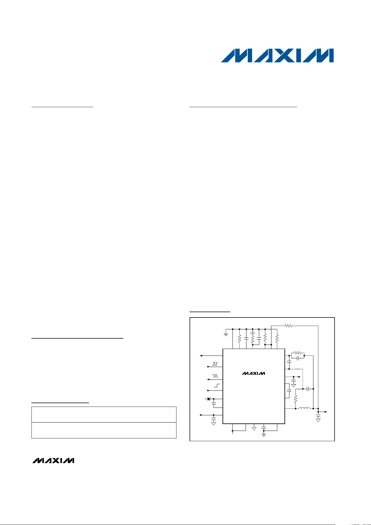
MAX8655
Highly Integrated, 25A, Wide-Input,
Internal MOSFET, Step-Down Regulator
________________________________________________________________ Maxim Integrated Products 1
Ordering Information
19-3982; Rev 0; 10/07
For pricing, delivery, and ordering information, please contact Maxim Direct at 1-888-629-4642,
or visit Maxim’s website at www.maxim-ic.com.
PART
TEMP
RANGE
PIN-
PACKAGE
PKG
CODE
MAX8655ETN+
-40°C to +85°C
56 TQFN - E P *
( 8mm x 8m m )
T5688M-4
Pin Configuration appears at end of data sheet.
MAX8655
REFIN
MODE
PGND
AVL
GND
OFF
ON
PVIN
INPUT 7V
TO 28V
SYNC OUTPUT
ENABLE INPUT
POWER-OK OUTPUT
FSYNC INPUT
OUTPUT
0.7V TO 12V
UP TO 25A
LX
VL
AVL
VLGND
VL
IN
CS+
CS-
SCOMP
ILIM2
SS
COMP
FB
OVP
ILIM1
PVIN
LXB
SYNCO
FSYNC
POK
EN
BST
Typical Operating Circuit
+Denotes a lead-free package.
*EP = Exposed pad.
Page 2
MAX8655
Highly Integrated, 25A, Wide-Input,
Internal MOSFET, Step-Down Regulator
2 _______________________________________________________________________________________
ABSOLUTE MAXIMUM RATINGS
ELECTRICAL CHARACTERISTICS
(VIN= 12V, V
BST
- VLX= 6.5V, TA= -40°C to +85°C, circuit of Figure 4, typical values are at TA= +25°C, unless otherwise noted.) (Note 2)
Stresses beyond those listed under “Absolute Maximum Ratings” may cause permanent damage to the device. These are stress ratings only, and functional
operation of the device at these or any other conditions beyond those indicated in the operational sections of the specifications is not implied. Exposure to
absolute maximum rating conditions for extended periods may affect device reliability.
PVIN, IN, EN to GND ..............................................-0.3V to +30V
BST to LXB ............................................................-0.3V to +7.5V
LX, LXB to GND............ (-2.5V for < 50ns transient) -1V to +30V
ILIM2, ILIM1, SYNCO, FSYNC, OVP,
SCOMP to GND .....................................-0.3V to (V
AVL
+ 0.3V)
VL to PGND ...........................................................-0.3V to +7.5V
AVL, FB, POK, COMP, SS, MODE, REFIN to GND ..-0.3V to +6V
CS+, CS- to GND ....................................................-0.3V to +6V
PGND to GND to VLGND ......................................-0.3V to +0.3V
Operating Junction Temperature Range.......... -40°C to +125°C
Junction Temperature......................................................+150°C
θJC(thermal resistance from
junction to exposed pad) (Note 1) ...............................3.5°C/W
θ
JT
(thermal resistance from junction to the top) ............3.9°C/W
I
LX (RMS)
.................................................................................27A
Storage Temperature Range .............................-65°C to +150°C
Lead Temperature (soldering, 10s) .................................+300°C
PARAMETER CONDITIONS
MIN TYP MAX UNITS
PVIN Operating Voltage Range 3 25 V
IN Operating Voltage Range VL = IN for V
IN
< 7V 4.5
25.0
V
IN Quiescent Supply Current V
FB
= 0.75V, no switching 2 3 mA
EN = GND, V
IN
≤ 28V 10
Shutdown Supply Current
I
IN
+ IVL + I
AVL
, EN = GND, V
AVL
= VVL = VIN = 5V 32
µA
PVIN Shutdown Supply Current V
PVIN
= VLX = V
BST
1 µA
AVL Undervoltage-Lockout
Threshold
V
AVL
rising, 3% typical hysteresis
3.90 4.15 4.40
V
Output-Voltage Adjust Range
Minimum output voltage is limited by minimum duty cycle
and external components
0.7 5.5 V
VL Regulation Voltage 7V < V
IN
< 28V 6.0 6.5 7.0 V
AVL Regulation Voltage 5.5V < V
VL
< 7V, 1mA < I
LOAD
< 10mA
4.900 4.975 5.050
V
AVL Output Current 10 mA
SOFT-START
SS Shutdown Resistance From SS to GND, V
EN
= 0V 20 100 Ω
SS Soft-Start Current V
REF
= 0.625V 18 23 28 µA
REFIN INPUT
REFIN Dual Mode™ Threshold
V
AVL
-
1.0V
V
AVL
V
REFIN Input Bias Current V
REFIN
= 0.7V to 1.5V
-250
+250
nA
REFIN Input Voltage Range 0 1.5 V
Dual Mode is a trademark of Maxim Integrated Products, Inc.
Note 1: Package thermal resistances were obtained using the method described in JEDEC specification JESD51-7, using a 4-layer
board. For detailed information on package thermal considerations, see www.maxim-ic.com/thermal-tutorial
.
Page 3
MAX8655
Highly Integrated, 25A, Wide-Input,
Internal MOSFET, Step-Down Regulator
_______________________________________________________________________________________ 3
ELECTRICAL CHARACTERISTICS (continued)
(VIN= 12V, V
BST
- VLX= 6.5V, TA= -40°C to +85°C, circuit of Figure 4, typical values are at TA= +25°C, unless otherwise noted.) (Note 2)
PARAMETER CONDITIONS MIN
TYP
MAX
UNITS
ERROR AMPLIFIER
REFIN = AVL
0.693
0.7
0.707
FB Regulation Voltage
V
REFIN
= 0.7V to 1.5V
V
RE F IN
-
0.00375
V
REFIN
V
RE FIN
+
0.00375
V
Transconductance 70 110 160 µS
COMP Shutdown Resistance From COMP to GND, V
EN
= 0V 20 100 Ω
FB Input Leakage Current V
FB
= 0.7V 5 50 nA
FB Input Common-Mode Range -0.1
+1.5
V
CURRENT-SENSE AMPLIFIER
V
OUT
= 0 to 5.5V 12
V/V
Voltage Gain
V
C S +
- V
C S -
= 30m V
Part to part variation at T
A
= +85°C
-4 +4 %
CURRENT LIMIT
R
ILIM1
= 24kΩ
27.2
32
36.8
Peak Current-Limit
Threshold (V
CS+
- V
CS-
)
ILIM1 = AVL 60 80 92
mV
Negative Current Limit % of valley current limit -90
-120 -150
%
CS+, CS- Input Bias Current V
CS+
= V
CS-
= 0 or 5.5V -25 +25 µA
CS+, CS- Input Common-Mode
Range
0 5.5 V
SLOPE COMPENSATION
V
SCOMP
= 2.5V
231.25 250.00 268.75
V
SCOMP
= 1.25V
113.77 123.00 132.23
SCOMP = AVL
231.25 250.00 268.75
T
A
= 0°C to +85°C
113.77 123.00 132.23
Slope Compensation at Maximum
Duty Cycle
SCOMP = GND
T
A
= -40°C to +85°C
110.70 123.00 132.23
mV
SCOMP High Threshold
V
AVL
-
0.5
V
SCOMP Low Threshold 0.5 V
SCOMP Adjustment Range
1.25
2.50
V
SCOMP Input Leakage Current V
SCOMP
= 1.25V to 2.5V 5 200 nA
Page 4
MAX8655
Highly Integrated, 25A, Wide-Input,
Internal MOSFET, Step-Down Regulator
4 _______________________________________________________________________________________
ELECTRICAL CHARACTERISTICS (continued)
(VIN= 12V, V
BST
- VLX= 6.5V, TA= -40°C to +85°C, circuit of Figure 4, typical values are at TA= +25°C, unless otherwise noted.) (Note 2)
PARAMETER CONDITIONS
MIN TYP MAX
UNITS
OSCILLATOR
R
FSYNC
= 21.0kΩ
800 1000 1200
Switching Frequency
R
FSYNC
= 143kΩ
160 200
240
kHz
Minimum Off-Time Measured at LX
235
ns
Minimum On-Time Measured at LX 75 100 ns
FSYNC Synchronization Range
160
1200
kHz
FSYNC Input High Pulse Width
100
ns
FSYNC Input Low Pulse Width
100
ns
FSYNC Rise/Fall Time 100 ns
SYNCO Phase Shift
180
D eg r ees
SYNCO Output Low Level I
SYNCO
= 5mA 0.4 V
SYNCO Output High Level I
SYNCO
= -5mA V
AV L
- 1V V
FSYNC Input Low 0.4 V
FSYNC Input High 2.5 V
THERMAL PROTECTION
Thermal Shutdown Rising temperature
+160
°C
Thermal-Shutdown Hysteresis 15 °C
POK
REFIN = AVL, V
FB
rising, typical hysteresis is 3%
629 650
671 mV
POK Threshold
V R E F IN = 0.75V to 1.5V , V F B r i si ng , typ i cal hyster esi s i s 3% 88.7 91.7 94.7
%
POK Output Voltage, Low V
FB
= 0.6V, I
POK
= 2mA
25 200 mV
POK Leakage Current, High V
POK
= 5.5V 1 µA
OVP
REFIN = AVL
770 800
840 mV
OVP Threshold Voltage
V
REFIN
= 0.7V to 1.5V
110 115
120 %
OVP, Leakage Current, High V
OVP
= 0.8V 500 nA
MODE CONTROL
MODE Logic-Level Low 4.5V ≤ V
AVL
≤ 5.5V 0.4 V
MODE Logic-Level High 4.5V ≤ V
AVL
≤ 5.5V 1.8 V
MODE Input Current V
MODE
= 0 to V
AVL
-1
+1
µA
SHUTDOWN CONTROL
EN Logic-Level Low 4.5V ≤ V
AVL
≤ 5.5V
0.45
V
EN Logic-Level High 4.5V ≤ V
AVL
≤ 5.5V 2 V
V
EN
= 0V -1
+1
EN Input Current
V
EN
= 28V 1.5 6.0
µA
Note 2: Specifications are 100% production tested at TA= +85°C. Limits over the operating temperature range are guaranteed by
design.
Page 5
MAX8655
Highly Integrated, 25A, Wide-Input,
Internal MOSFET, Step-Down Regulator
_______________________________________________________________________________________ 5
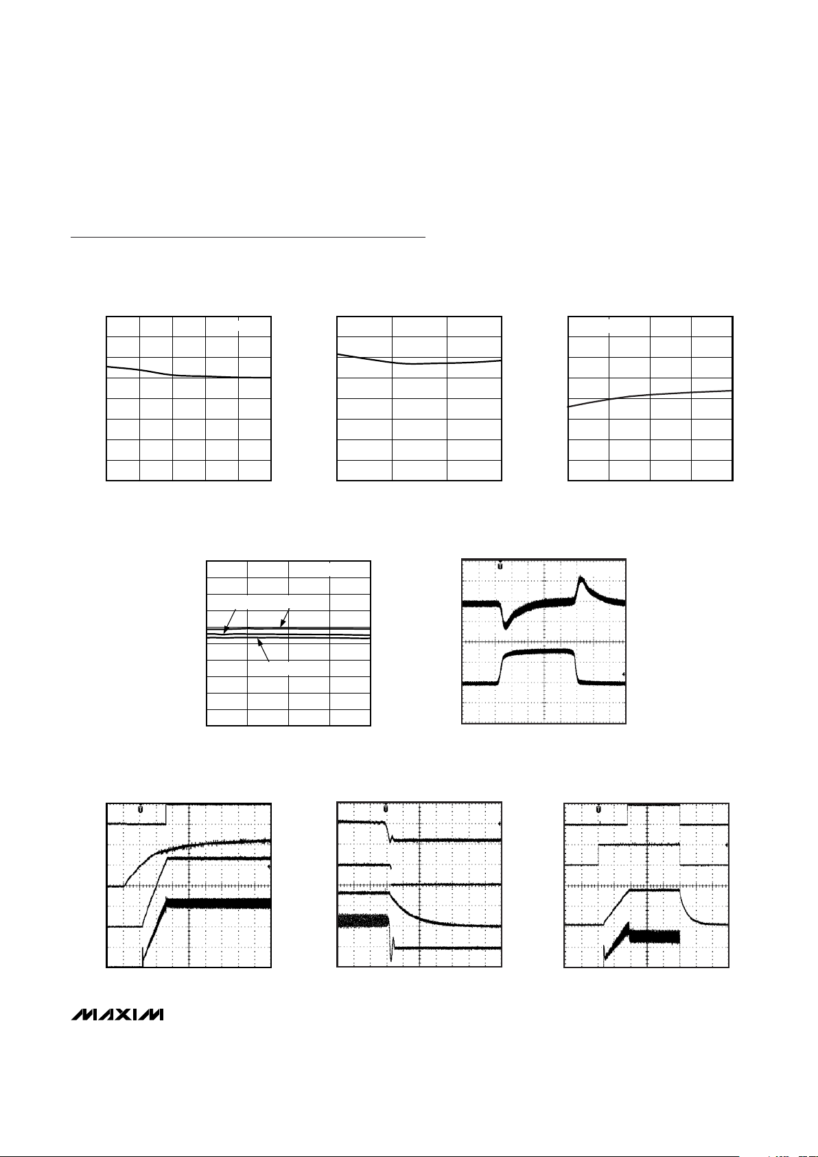
Typical Operating Characteristics
(TA = +25°C, unless otherwise noted.)
Typical Operating Characteristics
(TA = +25°C, unless otherwise noted.)
LOAD REGULATION
(CIRCUIT OF FIGURE 4)
LOAD CURRENT (A)
OUTPUT VOLTAGE (V)
MAX8655 toc01
0 5 10 15 20 25
3.26
3.27
3.28
3.29
3.30
3.31
3.32
3.33
3.34
VIN = 12V
LINE REGULATION
(CIRCUIT OF FIGURE 4)
INPUT VOLTAGE (V)
OUTPUT VOLTAGE (V)
MAX8655 toc02
5 101520
3.26
3.27
3.28
3.29
3.30
3.31
3.32
3.33
3.34
12A LOAD
FB VOLTAGE vs. EXPOSED PAD TEMPERATURE
(CIRCUIT OF FIGURE 4)
EXPOSED PAD TEMPERATURE (°C)
FB VOLTAGE (V)
MAX8655 toc03
-40 0 40 80 120
0.680
0.685
0.690
0.695
0.700
0.705
0.710
0.715
0.720
7.5A LOAD
OSCILLATOR FREQUENCY vs. INPUT VOLTAGE
(CIRCUIT OF FIGURE 4)
INPUT VOLTAGE (V)
OSCILLATOR FREQUENCY (kHz)
MAX8655 toc04
8 13182328
300
310
320
330
340
350
360
370
380
390
400
TA = -40°C
TA = +25°C
TA = +85°C
R
FSYNC
= 76.8kΩ
I
OUT
5A/div
0A
V
OUT
50mV/div
(AC-COUPLED)
40
μ
s/div
STEP-LOAD RESPONSE
(CIRCUIT OF FIGURE 3)
MAX8655 toc05
V
OUT
= 1.2V
V
IN
I
LX
10V/div
1V/div
5A/div
2ms/div
POWER-UP WAVEFORMS
(CIRCUIT OF FIGURE 4)
MAX8655 toc06
V
POK
V
OUT
5V/div
V
POK
I
LX
10V/div
2V/div
10A/div
200μs/div
POWER-DOWN WAVEFORMS
(CIRCUIT OF FIGURE 4)
MAX8655 toc07
V
IN
V
OUT
5V/div
V
EN
I
LX
5V/div
2V/div
10A/div
2ms/div
ENABLE WAVEFORMS
(CIRCUIT OF FIGURE 4)
MAX8655 toc08
V
POK
V
OUT
5V/div
Page 6
MAX8655
Highly Integrated, 25A, Wide-Input,
Internal MOSFET, Step-Down Regulator
6 _______________________________________________________________________________________
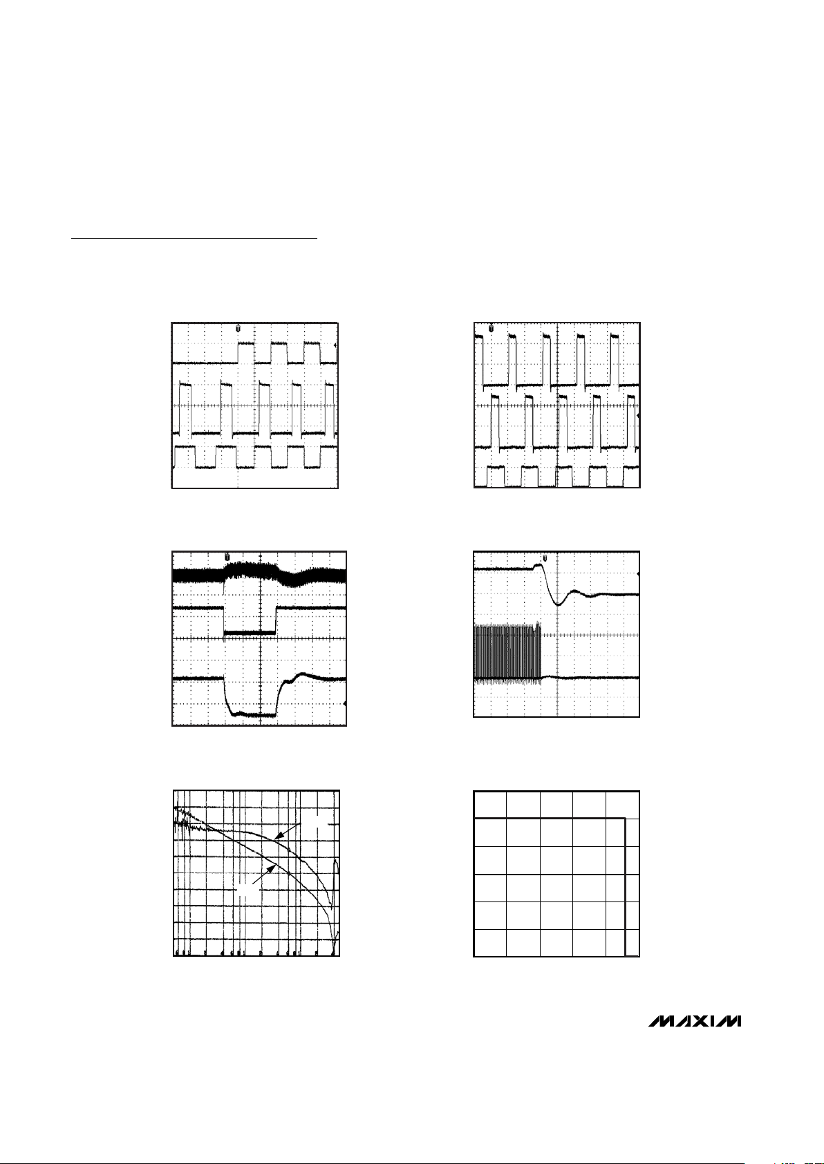
Typical Operating Characteristics (continued)
(TA = +25°C, unless otherwise noted.)
V
SYNCO
V
FSYNC
V
LX
5V/div
5V/div
5V/div
1
μ
s/div
FSYNC AND SYNCO
(CIRCUIT OF FIGURE 4)
MAX8655 toc09
INTERNAL 350kHz
OPERATION
SYNCHRONIZED TO
EXTERNAL 500kHz CLOCK
V
SYNCO
(MASTER)
V
LX
(SLAVE)
V
LX
(MASTER)
5V/div
5V/div
5V/div
1
μ
s/div
DUAL-PHASE SWITCHING
(CIRCUIT OF FIGURE 5)
MAX8655 toc10
I
IN
V
IN
V
OUT
500mV/div
(AC-COUPLED)
1V/div
1A/div
1ms/div
SHORT CIRCUIT AND RECOVERY
MAX8655 toc11
V
OUT
V
LX
2V/div
5V/div
40μs/div
OVERVOLTAGE PROTECTION
(CIRCUIT OF FIGURE 3)
MAX8655 toc12
CLOSED-LOOP BODE PLOT
(CIRCUIT OF FIGURE 3)
MAX8655toc13
50
500 1k 2k 4k 10k 20k
FREQUENCY (Hz)
GAIN (dB)
PHASE MARGIN (DEGREES)
40k 100k 200k400k
40
30
20
10
0
180
144
108
72
36
0
-10
-20
-30
-40
GAIN
PHASE
SAFE OPERATING AREA
INPUT VOLTAGE (V)
OUTPUT CURRENT (A)
MAX8655 toc14
5 1015202530
0
5
10
15
20
25
30
Page 7
MAX8655
Highly Integrated, 25A, Wide-Input,
Internal MOSFET, Step-Down Regulator
_______________________________________________________________________________________ 7
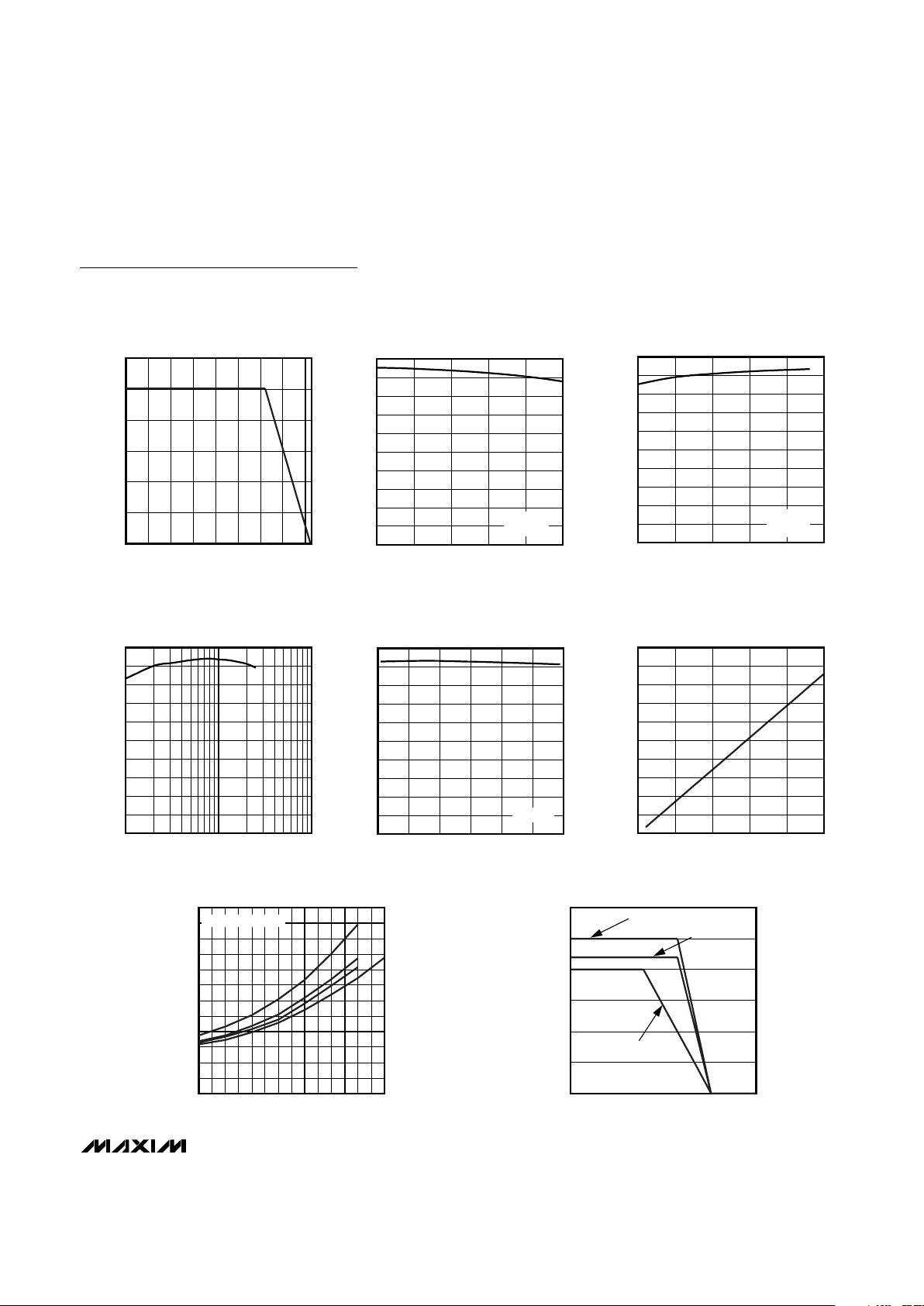
Typical Operating Characteristics (continued)
(TA= +25°C, unless otherwise noted.)
MAXIMUM OUTPUT CURRENT
vs. EXPOSED PAD TEMPERATURE
(CIRCUIT OF FIGURE 4)
EXPOSED PAD TEMPERATURE (°C)
OUTPUT CURRENT (A)
MAX8655 toc15
-40 80 10040020-20 60 120
0
5
10
15
20
25
30
EFFICIENCY vs. INPUT VOLTAGE
(CIRCUIT OF FIGURE 4)
INPUT VOLTAGE (V)
EFFICIENCY (%)
MAX8655 toc16
5 8 11 14 17 20
0
10
20
30
40
50
60
70
80
90
100
VO = 3.3V
10A LOAD
EFFICIENCY vs. OUTPUT VOLTAGE
(CIRCUIT OF FIGURE 4)
OUTPUT VOLTAGE (V)
EFFICIENCY (%)
MAX8655 toc17
1.0 1.5 2.0 2.5 3.0 3.5
0
10
20
30
40
50
60
70
80
90
100
12V INPUT
10A LOAD
EFFICIENCY vs. LOAD CURRENT
12V INPUT, 3.3V OUTPUT
(CIRCUIT OF FIGURE 4)
LOAD CURRENT (A)
EFFICIENCY (%)
MAX8655 toc18
0
10
20
30
40
50
60
70
80
90
100
1 10 100
EFFICIENCY vs. FREQUENCY
12.0V INPUT 3.3V OUTPUT
(CIRCUIT OF FIGURE 4)
FREQUENCY (kHz)
EFFICIENCY (%)
MAX8655 toc19
200 300 400 500 600 700 800
0
10
20
30
40
50
60
70
80
90
100
10A LOAD
R
VALLEY
vs. VALLEY CURRENT LIMIT
VALLEY CURRENT LIMIT (A)
R
VALLEY
(kΩ)
MAX8655 toc20
0 5 10 15 20 25
0
20
40
60
80
100
120
140
160
180
200
BOTTOM LAYER PCB TEMPERATURE vs.
OUTPUT CURRENT
I
OUT
(A)
BOTTOM PCB TEMPERATURE (°C)
MAX8655 toc21
0 5 10 15 20 25
0
120
80
20
100
40
60
VIN = 12V, VCC = 1.2V
OUTPUT-CURRENT CAPABILITY
vs. AMBIENT TEMPERATURE
AMBIENT TEMPERATURE (°C)
OUTPUT-CURRENT CAPABILITY (A)
MAX8655 toc22
-40 -25 -10 5 20 35 50 65 80 95 110 125
0
30
20
5
25
10
15
300 LFM
100 LFM
NO AIRFLOW
Page 8
MAX8655
Highly Integrated, 25A, Wide-Input,
Internal MOSFET, Step-Down Regulator
8 _______________________________________________________________________________________
Pin Description
PIN NAME FUNCTION
1–5, 51–56
PVIN
Power-Input Supply. PVIN connects to the drain of the internal high-side MOSFET. Connect inputdecoupling capacitors as close as possible between PVIN and PGND.
6, 16–21 LX
External Inductor Connection. Connect to the external power inductor. Leave pin 6 unconnected for
best routing.
7–15 PGND
Power Ground Connection from Source of Internal Low-Side MOSFET. Connect input-decoupling
capacitors as close as possible between PVIN and PGND.
22 VLGND Return for Low-Side MOSFET Gate-Driver Current
23, 28, 39,
48
GND
Analog Ground. Connect all pins to the analog ground plane, and connect the analog and power
ground planes together at the negative terminal of the output capacitor. Low-current signals return to
GND. Pin 28 must be connected externally to GND-EP, the analog ground plane.
24 VL
Internal 6.5V Linear-Regulator Output. Connect a 2.2µF to 10µF ceramic capacitor from VL to VLGND.
For V
IN
< 7V, connect VL directly to IN. VL supplies power for the internal gate drivers. VL is the input
to the AVL internal linear regulator.
25 IN
Input Supply Voltage. IN is the input to the VL linear regulator. Connect VL to IN for V
IN
< 7V.
Decouple to PGND with a 0.22µF ceramic capacitor.
26 EN
Enable. Apply logic-high to EN to enable the output, or logic-low to place the regulator in low-power
shutdown mode. Connect EN to IN for always-on operation.
27 AVL
Internal 5V Linear-Regulator Output. AVL powers the MAX8655’s internal circuits. Connect a 1µF
ceramic capacitor from AVL to GND.
29, 30, 42, 49
N.C. No Connection. Not internally connected.
31 CS+ Positive Differential Current-Sense Input
32 CS- Negative Differential Current-Sense Input
33 ILIM1
Analog Programmable Current-Limit Input for Inductor Current. Connect a resistor from ILIM1 to GND
to set the overcurrent threshold. ILIM1 sources 10µA through the resistor, and the voltage at ILIM1 is
attenuated 7.5:1 to set the final current limit. For example, a 60kΩ resistor results in 600mV at ILIM1.
This results in a current-limit threshold (V
CS+
- V
CS-
) of 80mV. The ILIM1 resistor range is 24kΩ to
60kΩ. Connect ILIM1 to AVL to set the default threshold of 80mV.
34 OVP
Output-Voltage Sensing for Overvoltage Protection. Connect OVP to the center of a resistor-divider
connected between the output of the regulator and GND to set the FB independent output
overvoltage trip point. Connect OVP to FB if this independence is not desired. The OVP threshold is
1.15 times the nominal feedback regulation voltage.
35 FB
Feedback Input. Connect FB to the center of a resistor voltage-divider connected between the output
and GND to set the output voltage. FB regulates to 0.7V or V
REFIN
.
36 COMP
Loop Compensation. Connect COMP to an external RC network to compensate the loop. COMP is
internally pulled to GND through 20Ω during shutdown.
37 SS
Soft-Start. Connect a 0.01µF to 1µF ceramic capacitor from SS to GND. This capacitor sets the softstart period during startup. See the Startup and Soft-Start section for more details. SS is internally
pulled to GND through 20Ω during shutdown.
38 REFIN
External Reference Input. Connect REFIN to AVL to use the internal 0.7V reference for the feedback
threshold.
Page 9

MAX8655
Highly Integrated, 25A, Wide-Input,
Internal MOSFET, Step-Down Regulator
_______________________________________________________________________________________ 9
Pin Description (continued)
PIN NAME FUNCTION
40 ILIM2
Programmable Current-Limit Input. Connect a resistor from ILIM2 to GND to set the valley current
limit. See the Setting the Current Limit section.
41 SCOMP
Programmable Slope-Compensation Input. Internal slope-compensation voltage rate is the voltage at
SCOMP times 0.1 divided by the oscillator period (T). Connect SCOMP to AVL or GND to set to the
default of 250mV/T or 125mV/T, respectively.
43 POK
Open-Drain Power-OK Output. POK goes high impedance when the output voltage rises above 91%
of the nominal regulation voltage. POK pulls low during shutdown or when the output drops below
88% of the nominal regulation voltage.
44 FSYNC
Frequency Set and Synchronization Input. Connect a resistor from FSYNC to GND to set the switching
frequency, or drive with a clock signal to synchronize between 160kHz and 1.2MHz. See the
Switching Frequency and Synchronization section.
45 MODE
Current-Limit Operating Mode Selection. Connect MODE to AVL for latch-off current limit or connect
MODE to GND for automatic recovery current limit.
46 SYNCO
Synchronization Output. Provides a clock output for synchronizing another MAX8655 with 180°
out-of-phase operation.
47 BST Boost Capacitor Connection. Connect a 0.22µF ceramic capacitor from BST to LXB.
50 LXB LX Boost Capacitor Connection. Connect a 0.22µF ceramic capacitor between LXB and BST.
— GND-EP Exposed Pad. Connect to GND externally. See the Pin Configuration.
— PVIN-EP Exposed Pad. Internally connected to PVIN. See the Pin Configuration.
— LX-EP Exposed Pad. Internally connected to LX. See the Pin Configuration.
Page 10

MAX8655
Highly Integrated, 25A, Wide-Input,
Internal MOSFET, Step-Down Regulator
10 ______________________________________________________________________________________
Figure 1. Functional Diagram
IN
6.5V LDO
REGULATOR
5V AVL
LDO
EN
PWM
CONTROL
LOGIC
SHOOT-THROUGH
PROTECTION
LEVEL
SHIFT
BST
SYNCO
FSYNC
MODE
CS+
CS-
ILIM1
GND
ILIM2
POK
CURRENT-LIMIT
CONTROL LOGIC
UVLO
VL
LX
÷7.5
10μA
VL
OVP
SCOMP
THERMAL
SHDN
COMP
PWM
COMPARATOR
REF
SELECT
LOGIC
SS
REFIN
SOFT-START
CIRCUITRY
FB
AVL
VL
VOLTAGE
REFERENCE
V
REF
V
SUM
VLGND
PGND
PVIN
MAX8655
COMP
CLAMP
OSCILLATOR
SLOPE
COMP
GM
ERROR
AMPLIFIER
OVP
1.15V REF
CURRENT-SENSE
AMPLIFIER
12
CURRENT-LIMIT
COMPARATOR
X1
LEVEL
SHIFT
FB
0.9V REF
Page 11

MAX8655
Highly Integrated, 25A, Wide-Input,
Internal MOSFET, Step-Down Regulator
______________________________________________________________________________________ 11
Detailed Description
DC-DC Converter Control Architecture
The MAX8655 step-down regulator uses a PWM, peak
current-mode control scheme. An internal transconductance amplifier establishes an integrated error voltage.
The heart of the PWM controller is a PWM comparator
that compares the integrated voltage-feedback signal
against the amplified current-sense signal plus an
adjustable slope-compensation ramp, which is
summed with the current signal to ensure stability. At
each rising edge of the internal clock, the internal highside MOSFET turns on until the PWM comparator trips
or the maximum duty cycle is reached. During this ontime, current ramps up through the inductor, storing
energy in the output inductor while sourcing current to
the output. The current-mode feedback system regulates the peak inductor current as a function of the output-voltage error signal. The circuit acts as a
switch-mode transconductance amplifier and pushes
the output LC filter pole normally found in a voltagemode PWM to a higher frequency. Figure 1 is the functional diagram.
During the second half of the cycle, the internal highside MOSFET turns off and the internal low-side MOSFET turns on. The output inductor releases the stored
energy as the current ramps down, providing current to
the load. The output capacitor stores charge when the
inductor current exceeds the required load current and
discharges when the inductor current is lower, smoothing the voltage across the load. Under soft-overload
conditions, when the peak inductor current exceeds the
selected current limit (see the Current-Limit Circuit section), the high-side MOSFET is turned off immediately
and the low-side MOSFET is turned on and remains on
to let the inductor current ramp down until the next
clock cycle. Under severe-overload or short-circuit conditions, the valley foldback current limit is enabled to
reduce power dissipation of external components.
The MAX8655 operates in a forced-PWM mode. As a
result, the regulator maintains a constant switching frequency, regardless of load, to allow for easier filtering
of the switching noise.
Internal Linear Regulators
The MAX8655 contains two internal LDO regulators.
The AVL regulator provides 5V for the IC’s internal circuitry, and the VL regulator provides 6.5V for the MOSFET gate drivers. Connect a 2.2µF ceramic capacitor
from VL to VLGND, and connect a 1µF ceramic capacitor from AVL to GND. The AVL regulator input is internally connected to the VL regulator output. For 5V input
applications, connect VL directly to IN and connect a
10Ω resistor from VL to AVL.
Undervoltage Lockout
When V
AVL
drops below 4.03V, the MAX8655 assumes
that the supply voltage is too low to make valid decisions, so the undervoltage-lockout (UVLO) circuitry
inhibits switching and turns off both internal power
MOSFETs. When V
AVL
rises above 4.15V, the regulator
enters the startup sequence and then resumes normal
operation.
Startup and Soft-Start
The internal soft-start circuitry gradually ramps up the
reference voltage to control the rate of rise of the output
voltage and reduce input surge currents during startup.
The soft-start period is determined by the value of the
capacitor from SS to GND. The soft-start time is
approximately (30.4ms/µF) x CSS. The MAX8655 also
features monotonic output-voltage rise; therefore, both
power MOSFETs are kept off if the voltage at FB is
higher than the voltage at SS. This allows the MAX8655
to start up into a prebiased output without pulling the
output voltage down.
Before the MAX8655 begins the soft-start and powerup sequence, the following conditions must be met:
•V
AVL
exceeds the 4.15V UVLO threshold.
• EN is at logic-high.
• The thermal limit is not exceeded.
Enable
The MAX8655 features a low-power shutdown mode. A
logic-low at EN shuts down the regulator. During shutdown, the output is high impedance. Shutdown
reduces the IN current to less than 10µA. A logic-high
at EN enables the regulator.
Page 12

MAX8655
Highly Integrated, 25A, Wide-Input,
Internal MOSFET, Step-Down Regulator
12 ______________________________________________________________________________________
High-Side Gate-Drive Supply (BST)
A flying capacitor boost circuit (Figure 2) generates the
gate-drive voltage for the internal high-side n-channel
MOSFET. The capacitor between BST and LXB is
charged from VL to 6.5V minus the diode forward-voltage drop while the low-side MOSFET is on. When the
low-side MOSFET is switched off, the stored voltage of
the capacitor is stacked above LXB to provide the necessary turn-on voltage (VGS) for the high-side MOSFET.
An internal switch between BST and the internal highside MOSFET’s gate closes to turn the MOSFET on.
Current-Sense Amplifier
The current-sense circuit amplifies the differential current-sense voltage (V
CS+
- V
CS-
). This amplified current-sense signal and the internal-slope-compensation
signal are summed (V
SUM
) together and fed into the
PWM comparator’s inverting input. The PWM comparator shuts off the high-side MOSFET when V
SUM
exceeds the integrated feedback voltage (V
COMP
).
The differential current sense is also used to provide
peak inductor current limiting. This current limit is more
accurate than the valley current limit, which is measured
across the internal low-side MOSFET.
Current-Limit Circuit
The MAX8655 uses both foldback and peak current limiting. The valley foldback current limit is used to reduce
power dissipation of external components—mainly the
inductor, internal power MOSFETs, and the upstream
power source, when the output is severely overloaded
or short circuited and when POK is low. Thus, the circuit
can withstand short-circuit conditions continuously without causing overheating of any component. The peak
constant current limit sets the current-limit point more
accurately since it does not have to suffer the wide variation of the low-side power MOSFET’s on-resistance
due to tolerance and temperature.
The valley current is sensed across the on-resistance of
the low-side MOSFET. The valley current limit trips when
the sensed current exceeds the valley current limit.
Set the minimum valley current limit when the output
voltage is at its nominal regulated value, higher than
the maximum peak current-limit setting. With this
method, the current-limit point accuracy is controlled
by the peak current limit and is not interfered with by
the wide variation of the MOSFET’s on-resistance. See
the Setting the Current Limit section for how to set
these limits.
The MAX8655 can be configured for either an
adjustable valley current-limit threshold with adjustable
foldback ratio or a fixed valley current limit that latches
the regulator off. To use foldback current limit with
autorecovery, connect MODE to GND. When the latch-off
mode is used, connect MODE to AVL and set the current-limit threshold with one resistor from ILIM2 to GND.
Cycle EN or input power to reset the current-limit latch.
The peak current limit is used to sense the inductor current, and is more accurate than the valley current limit
because it does not depend upon the on-resistance of
the low-side MOSFET. The peak current can be measured across the resistance of the inductor for the highest efficiency, or alternatively, a current-sense resistor
can be used for more accurate current sensing. A
resistor connected from ILIM1 to GND sets the peak
current-limit threshold.
For more information on the current limit, see the
Setting the Current Limit section.
Switching Frequency and Synchronization
The MAX8655 has an adjustable internal oscillator that
can be set to any frequency from 200kHz to 1MHz. To
set the switching frequency, connect a resistor from
FSYNC to GND.
The MAX8655 can also be synchronized to an external
clock by connecting the clock signal to FSYNC. A synchronization output (SYNCO) is provided to synchronize
a second MAX8655 180° out-of-phase with the first by
connecting SYNCO of the first MAX8655 to FSYNC of the
second. When the first MAX8655 is synchronized to an
external clock, the external clock is inverted to generate
SYNCO. Therefore, to get 180° out-of-phase operation
with an external clock, the clock input to the first
MAX8655 should have a 50% duty cycle. Figure 3 is the
single-phase, 600kHz switching, 10.8V to 13.2V input
and 1.2V/20A output. Figure 4 shows single-phase,
350kHz switching, 6V to 20V input, and 3.3V/20A output.
VL
BST
LXB
MAX8655
Figure 2. High-Side Gate Boost Circuit
Page 13

MAX8655
Highly Integrated, 25A, Wide-Input,
Internal MOSFET, Step-Down Regulator
______________________________________________________________________________________ 13
REFIN
The MAX8655 has a reference input (REFIN). When an
external reference up to 1.5V is connected to REFIN,
the feedback regulation voltage is equal to the voltage
applied to REFIN.
Connect REFIN to AVL to use the internal 0.7V reference.
Overvoltage Protection
The MAX8655 provides output overvoltage protection
(OVP). The OVP threshold is set independent of the
output regulation voltage with a resistor voltage-divider.
When the voltage at OVP exceeds the OVP threshold,
the regulator stops switching and latches on the lowside power MOSFET. Cycle EN or the power applied to
AVL to clear the latch.
Power-Good Signal (POK)
POK is an open-drain output on the MAX8655 that monitors the output voltage. When the output is above 92%
of its nominal regulation voltage, POK is high impedance. When the output drops below 89% of its nominal
regulation voltage, POK is internally pulled low. POK is
also internally pulled low when the MAX8655 is shut
down or in a fault condition.
Thermal-Overload Protection
Thermal-overload protection limits total power dissipation in the MAX8655. When the junction temperature
exceeds +160°C, an internal thermal sensor shuts
down the device, allowing the IC to cool. The thermal
sensor turns the IC on again after the junction temperature cools by 15°C, resulting in a pulsed output during
continuous thermal-overload conditions.
MAX8655
PVIN
PVIN
PVIN
PVIN
PVIN
LX
PGND
PGND
PGND
PGND
PGND
PGND
PGND
PGND
PGND
LX
LX
LX
LX
LX
OFF
ON
PVIN
C14
1μF
C8
0.47μF
C10
100pF
C12
470pF
C13
0.022μF
C15
0.22μF
C1–C3
3 x 10μF
CERAMIC
C16
0.22μF
R1
681Ω
R3
2.87kΩ
R12
80.6kΩ
R2
357Ω
R9
56.2kΩ
R7
40.2kΩ
L1
0.56μH
1.8mΩ
C18
2.2μF
R8
41.2kΩ
R13
100kΩ
R10
51.1kΩ
C9
0.47μF
C6–C20
4 x 100μF
CERAMIC
ENABLE
INPUT
INPUT
11.8V TO 13.2V
FOR INTERNAL
OSCILLATOR
OPERATION ONLY
POWER-OK OUTPUT
FSYNC INPUT
SYNC OUTPUT
OUTPUT 1.2V
UP TO 20A
AVL
D1
VL
AVL
LX
VLGND
GND
VL
IN
EN
AVL
GND
SCOMP
ILIM2
GND
REFIN
SS
COMP
FB
OVP
ILIM1
CS-
CS+
N.C.
N.C.
PVIN
PVIN
PVIN
PVIN
PVIN
PVIN
LXB
N.C.
GND
BST
SYNCO
MODE
FSYNC
POK
R5
4.02kΩ
Figure 3. Single-Phase, 600kHz Switching, 10.8V to 13.2V Input, and 1.2V/20A Output
Page 14

MAX8655
Highly Integrated, 25A, Wide-Input,
Internal MOSFET, Step-Down Regulator
14 ______________________________________________________________________________________
Design Procedure
Setting the Output Voltage
To set the output voltage for the MAX8655, connect FB
to the center of an external resistor-divider from the output to GND (R3 and R5 of Figure 5). Select R5 between
5kΩ and 24kΩ, and then calculate R3 with the following
equation:
where V
FB
= 0.7V or V
REFIN
. R3 and R5 should be
placed as close as possible to the IC.
RR
V
V
OUT
FB
35 1=× −
⎛
⎝
⎜
⎞
⎠
⎟
MAX8655
PVIN
PVIN
PVIN
PVIN
PVIN
LX
PGND
PGND
PGND
PGND
PGND
PGND
PGND
PGND
PGND
LX
LX
LX
LX
LX
OFF
ON
PVIN
C14
1μF
C8
0.22μF
C10
100pF
C12
560pF
C13
0.022μF
C15
0.22μF
C1–C5
5 x 10μF
CERAMIC
C16
0.22μF
R1
1.74kΩ
R4
11.5kΩ
R3
11.5kΩ
R2
3.57kΩ
R9
71.5kΩ
R7
243kΩ
R6
3.09kΩ
L1
1μH
1.6mΩ
C18
2.2μF
R8
76.8kΩ
R13
100kΩ
R14
13kΩ
R11
140kΩ
C9
0.22μF
ENABLE
INPUT
INPUT 6V TO 20V
FOR INTERNAL
OSCILLATOR
OPERATION ONLY
POWER-OK OUTPUT
FSYNC INPUT
SYNC OUTPUT
OUTPUT 3.3V
UP TO 20A
AVL
AVL
D1
VL
AVL
LX
VLGND
GND
VL
IN
EN
AVL
GND
SCOMP
ILIM2
REFIN
SS
COMP
FB
OVP
ILIM1
CS-
CS+
N.C.
N.C.
PVIN
PVIN
PVIN
PVIN
PVIN
PVIN
LXB
N.C.
GND
BST
SYNCO
MODE
FSYNC
POK
GND
R12
10kΩ
C6–C19
3 x 220μF
15μΩ ESR
R5
3.09kΩ
Figure 4. Single-Phase, 350kHz Switching, 6V to 20V Input, and 3.3V/20A Output
MAX8655
LX
R5
R3
FB
Figure 5. Setting the Output Voltage with a Resistor VoltageDivider
Page 15

MAX8655
Highly Integrated, 25A, Wide-Input,
Internal MOSFET, Step-Down Regulator
______________________________________________________________________________________ 15
Setting the Output Overvoltage Protection
To set the overvoltage threshold voltage for the
MAX8655, connect OVP to the center of an external
resistor-divider connected between the output and GND
(R4 and R6 of Figure 3). Select R6 between 5kΩ and
24kΩ, then calculate R4 with the following equation:
where V
OVP
= 1.15 x VFB.
Inductor Selection
There are several parameters that must be examined
when determining which inductor is to be used. Input
voltage, output voltage, load current, switching frequency, and LIR. LIR is the ratio of the inductor current
ripple to the maximum DC load current. A higher LIR
value allows for a smaller inductor, but results in higher
losses and higher output ripple. A good compromise
between size and efficiency is an LIR of 0.3. Once all
the parameters are chosen, the inductor value is determined as follows:
where fS is the switching frequency. Choose a standard-value inductor close to the calculated value. The
exact inductor value is not critical and can be adjusted
to make trade-offs among size, cost, and efficiency.
Lower inductor values minimize size and cost, but they
also increase the output ripple and reduce the efficiency due to higher peak currents. On the other hand,
higher inductor values increase efficiency, but eventually resistive losses due to extra turns of wire exceed
the benefit gained from lower AC current levels. This is
especially true if the inductance is increased without
also increasing the physical size of the inductor. Find a
low-loss inductor having the lowest possible DC resistance that fits the allotted dimensions. The chosen
inductor’s saturation current rating must exceed the
peak inductor current determined as:
Setting the Switching Frequency
To set the switching frequency, connect a resistor from
FSYNC to GND. Calculate the resistor value in kΩ from
the following equation:
where fSis the desired switching frequency in kHz.
Setting the Slope Compensation
For most applications where the duty cycle is less than
40%, connect SCOMP to GND to set the internal slope
compensation to the default of 125mV/T, where T is the
oscillator period (T = 1 / fS).
For a slope compensation of 250mV/T, connect
SCOMP to AVL.
For applications with a duty cycle greater than 40%, set
the SCOMP voltage with a resistor voltage-divider from
AVL to GND (R11 and R12 in Figure 6). First, use the
following equation to find the SCOMP voltage:
where RLis the DC resistance of the inductor, V
IN_MIN
is the minimum operating input voltage, and fSis the
switching frequency.
Next, select a value for R11, typically 10kΩ, and solve
for R12 as follows:
This sets the internal slope-compensation voltage rate
to V
SCOMP
/ (10 x T).
R
VV R
V
SCOMP
SCOMP
12
511
=
−
()
×
V
R
fL
VV
SCOMP
L
S
OINMIN
=
×
×
×− ×
120
0 182(. )
_
R
f
FSYNC
S
=−
30600
9 914.
II
LIR
I
PEAK LOAD MAX LOAD MAX
=+×
() ()
2
L
VVV
V f I LIR
OUT IN OUT
IN S LOAD MAX
=
×−
×× ×
()
()
RR
V
V
OUT
OVP
46 1=× −
⎛
⎝
⎜
⎞
⎠
⎟
MAX8655
AVL
R11
R12
SCOMP
Figure 6. Resistor-Divider for Setting the Slope Compensation
Page 16

MAX8655
Highly Integrated, 25A, Wide-Input,
Internal MOSFET, Step-Down Regulator
16 ______________________________________________________________________________________
Setting the Current Limit
Valley Current Limit
The MAX8655 has an adjustable valley current limit, configurable for foldback with automatic recovery, or constant-current limit with latch-up. To set the constantcurrent limit for the latch-up mode, connect a single
resistor R
ILIM2
from ILIM2 to GND. For latch-up current-
limit mode, set R
ILIM2
equal to R
VALLEY
obtained from
the R
VALLEY
vs. Valley Current Limit graph in the Typical
Operating Characteristics section for the required valley
current I
VALLEY
. I
VALLEY
is the value of the inductor val-
ley current at maximum load (I
LOAD(MAX)
- 1/2 I
P-P
)
To set the current limit for foldback mode, connect a
resistor from ILIM2 to the output (R
FOBK
), and another
resistor from ILIM2 to GND (R
ILIM2
). See Figure 7. The
values of R
FOBK
and R
ILIM2
are calculated as follows.
First, select the percentage of foldback (PFB). This percentage corresponds to the current limit when V
OUT
equals zero divided by the current limit when V
OUT
equals its nominal voltage. A typical value of PFBis in
the 15% to 40% range. A lower value of PFByields
lower short-circuit current. The following equations are
used to calculate R
FOBK
and R
ILIM2
:
where I
ILIM2
is 5µA.
If the resulting value of R
ILIM2
is negative, increase PFB.
Peak Current Limit
The peak current-limit threshold (VTH) is set by a resistor
connected from ILIM1 to GND (R
ILIM1
). VTHcorresponds
to the peak voltage across the sensing element (inductor
or current-sense resistor). R
ILIM1
is calculated as follows:
This allows a maximum DC output current of:
where R
L
is the DC resistance of the inductor.
To ensure maximum output current, use the minimum
value of VTHfrom each setting, and the maximum R
L
values at the highest expected operating temperature.
The DC resistance of the inductor’s copper wire has a
+0.38%/°C temperature coefficient.
An RC circuit is connected across the inductor (see
Figure 8). The RC time constant is set to be 1.1 to 1.2
times the inductor (L/R
L
) time constant. Pick the value
of C9 in the 0.1µF to 0.47µF range, and then calculate
R1 from:
R1 = 1.2L / (R
L
x C9)
Add a resistor (R2 in Figure 8) to the CS- connection to
minimize input offset error. Calculate the value of R2 as
follows:
• When V
OUT
≥ 2.4V:
• When V
OUT
< 2.4V:
R
AxR
A
RxA
k
ILIM
2
15 1
15
10
32
1
=
μ
μ+
μ
Ω
⎛
⎝
⎜
⎞
⎠
⎟
R
A
RA
k
R
A
ILIM
2
20
10
32
1
20
1
=
+
×
⎛
⎝
⎜
⎞
⎠
⎟
×μ
μ
μ
Ω
I
V
R
I
LIM
THLPP
=−
−
2
R
V
A
ILIMTH1
75
10
=
×.
μ
R
IR R
VI R R
ILIM
ILIM VALLEY FOBK
OUT ILIM FOBK VALLEY
2
2
2
=
××
+× −
()
()
R
PV
IP
FOBK
FB OUT
ILIM FB
=
×
×−
()
2
1
MAX8655
LX
R
ILIM2
R
FOBK
ILIM2
OUT
Figure 7. ILIM2 Resistor Connections
MAX8655
LX
R2
R1
L1
C9
C10
CS+
CS-
V
OUT
C11
Figure 8. Current Sense Using the Inductor’s DC Resistance
Page 17

MAX8655
Highly Integrated, 25A, Wide-Input,
Internal MOSFET, Step-Down Regulator
______________________________________________________________________________________ 17
Capacitor C11 is connected in parallel with R2 and is
equal in value with C9.
Add a 100pF (C10) capacitor across the CS+ and CSinputs close to the IC.
Input Capacitor
The input filter capacitor reduces peak currents drawn
from the power source and reduces noise and voltage
ripple on the input caused by the circuit’s switching.
The input capacitors must meet the ripple-current
requirement (I
RMS
) imposed by the switching currents
defined by the following equation:
I
RMS
has a maximum value when the input voltage
equals twice the output voltage (VIN= 2 x V
OUT
), so
I
RMS(MAX)
= I
LOAD
/ 2. Ceramic capacitors are recommended due to the low ESR and ESL at high frequency
with relatively low cost. Choose a capacitor that
exhibits less than 10°C temperature rise at the maximum operating RMS current for optimum long-term reliability. Ceramic capacitors with an X5R or better
temperature characteristic are recommended.
Output Capacitor
The key selection parameters for the output capacitor
are the actual capacitance value, the equivalent series
resistance (ESR), the equivalent series inductance
(ESL), and the voltage-rating requirements. These
parameters affect the overall stability, output-voltage
ripple, and transient response. The output ripple has
three components: variations in the charge stored in
the output capacitor, the voltage drop across the
capacitor’s ESR, and ESL caused by the current into
and out of the capacitor. The maximum output-voltage
ripple is estimated as follows:
V
RIPPLE
= V
RIPPLE(ESR)
+ V
RIPPLE(C)
+ V
RIPPLE(ESL)
The output-voltage ripple as a consequence of the
ESR, ESL, and output capacitance is:
where I
P-P
is the peak-to-peak inductor current.
These equations are suitable for initial capacitor selection, but final values should be chosen based on a prototype or evaluation circuit. As a general rule, a smaller
current ripple results in less output-voltage ripple.
Since the inductor ripple current is a factor of the
inductor value and input voltage, the output-voltage ripple decreases with larger inductance, and increases
with higher input voltages. The MAX8655 is designed to
work with polymer, tantalum, aluminum electrolytic, or
ceramic output capacitors. The aluminum electrolytic
capacitor is the least expensive; however, it has higher
ESR. To compensate for this, use a ceramic capacitor
in parallel to reduce the switching ripple and noise.
Ceramic capacitors are recommended for high-frequency (500kHz to 1MHz) designs. For reliable and
safe operation, ensure that the capacitor’s voltage and
ripple-current ratings exceed the calculated values.
The response to a load transient depends on the
selected output capacitors. During a load transient, the
output voltage instantly changes by ESR x ΔI
LOAD
.
Before the regulator can respond, the output voltage
deviates further, depending on the inductor and outputcapacitor values. After a short time (see the Typical
Operating Characteristics section), the regulator
responds by regulating the output voltage back to its
nominal state. The regulator response time depends on
its closed-loop bandwidth. With a higher bandwidth,
the response time is faster, thus preventing the output
voltage from further deviation from its regulating value.
Compensation Design
The MAX8655 uses an internal transconductance error
amplifier whose output compensates the control loop.
The external inductor, output capacitor, compensation
resistor, and compensation capacitors determine the
loop stability. The inductor and output capacitor are chosen based on performance, size, and cost. Additionally,
the compensation resistor and capacitors are selected to
optimize control-loop stability. The component values,
shown in Figures 3 and 4, yield stable operation over the
given range of input-to-output voltages.
The regulator uses a current-mode control scheme that
regulates the output voltage by forcing the required current through the external inductor. The voltage drop
across the DC resistance of the inductor or the alternate
series current-sense resistor is used to measure the
inductor current. Current-mode control eliminates the
double pole in the feedback loop caused by the
I
VV
fLVV
PP
IN OUTSOUT
IN
−
=
−
×
×
V
I
Cf
RIPPLE C
PP
OUT S
()
=
××
−
8
V
V
L ESL
ESL
RIPPLE ESLIN()
=
+
×
V I ESR
RIPPLE ESR P P()
=×
−
I
IVVV
V
RMS
LOAD OUT IN OUT
IN
=
×−
()
Page 18

MAX8655
Highly Integrated, 25A, Wide-Input,
Internal MOSFET, Step-Down Regulator
18 ______________________________________________________________________________________
inductor and output capacitor resulting in a smaller
phase shift and requiring a less elaborate error-amplifier
compensation than voltage-mode control. A simple
series RCand CCis all that is needed to have a stable,
high-bandwidth loop in applications where ceramic
capacitors are used for output filtering. For other types
of capacitors, due to the higher capacitance and ESR,
the frequency of the zero created by the capacitance
and ESR is lower than the desired closed-loop crossover
frequency. To stabilize a nonceramic output-capacitor
loop, add another compensation capacitor from COMP
to GND to cancel this ESR zero. See Figure 9.
The basic regulator loop is modeled as a power modulator, an output feedback divider, and an error amplifier. The power modulator has DC gain G
MOD(dc)
, set by
gmcx R
LOAD
, with a pole and zero pair set by R
LOAD
,
the output capacitor (C
OUT
), and its equivalent series
resistance (ESR). Below are equations that define the
power modulator:
where R
LOAD
= V
OUT
/ I
OUT(MAX)
, fSis the switching
frequency, L is the output inductance, gmc= 1 / (A
VCS
x
R
L
), where A
VCS
is the gain of the current-sense amplifi-
er (12 typ), R
L
is the DC resistance of the inductor, the
duty cycle D = V
OUT
/ V
IN. KS
is a slope compensation
factor calculated from the following equation:
When SCOMP is connected to GND, use V
SCOMP
= 1.25V;
when SCOMP is connected to AVL, use V
SCOMP
= 2.5V.
Find the pole and zero frequencies created by the
power modulator as follows:
When C
OUT
comprises “n” identical capacitors in paral-
lel, the resulting C
OUT
= n x C
OUT(EACH)
, and ESR =
ESR
(EACH)
/ n. Note that the capacitor zero for a parallel combination of like capacitors is the same as for an
individual capacitor. Figure 10 is the simplified gain
plot for the f
zMOD
> fCcase.
The feedback voltage-divider has a gain of GFB= VFB/
V
OUT
, where VFBis equal to 0.7V.
The transconductance error amplifier has a DC gain,
G
EA(DC)
= g
mEA
x RO, where g
mEA
is the error-amplifi-
er transconductance, which is equal to 110µS, and R
O
is the output resistance of the error amplifier, which is
30MΩ. A dominant pole (f
pdEA
) is set by the compensation capacitor (CC), the amplifier output resistance
(RO), and the compensation resistor (RC); a zero (f
zEA
)
is set by the compensation resistor (RC) and the compensation capacitor (CC). There is an optional pole
(f
pEA
) set by CFand RCto cancel the output capacitor
ESR zero if it occurs near the crossover frequency (fC).
Thus:
f
CR
pEA
FC
=
××
1
2π
f
CR
zEA
CC
=
××
1
2π
f
CRR
pdEA
COC
=
×× +
1
2π ()
f
C ESR
zMOD
OUT
=
××
1
2π
f
RC
Lf C
KD
pMOD
LOAD OUT
S OUT
S
=
××
+
×× ×
××−−
[]
⎡
⎣
⎢
⎤
⎦
⎥
1
2
1
2
105
π
π
().
K
VLf
VVR
S
SCOMP S
IN O L
=+
××
×−×
1
120 ( )
Gg
R
R
Lf
KD
MOD dc mc
LOAD
LOAD
S
()
.
=×
+
×
××−
()
()
−
[]
⎡
⎢
1105
MAX8655
C
C
C
F
R
C
COMP
Figure 9. Compensation Components
GAIN
(dB)
FREQUENCY
fp
MOD
fz
MOD
fc
CLOSED LOOP
ERROR
AMPLIFIER
0dB
FB
DIVIDER
POWER
MODULATOR
Figure 10. Simplified Gain Plot for the f
zMOD
> fCCase
Page 19

MAX8655
Highly Integrated, 25A, Wide-Input,
Internal MOSFET, Step-Down Regulator
______________________________________________________________________________________ 19
The crossover frequency, fC, should be much higher
than the power-modulator pole f
PMOD
. Also, fCshould
be less than or equal to 1/5 the switching frequency.
Select a value for fCin the range:
At the crossover frequency, the total loop gain must
equal 1, and is expressed as:
For the case where f
zMOD
is greater than fC:
Then RCcan be calculated as:
where g
mEA
= 110µS.
The error-amplifier compensation zero formed by R
C
and CCshould be set at the modulator pole f
PMOD
.
Calculate the value of C
C
as follows:
If f
zMOD
is less than 5 x fC, add a second capacitor C
F
from COMP to GND. The value of CFis:
As the load current decreases, the modulator pole
also decreases; however, the modulator gain increases
accordingly and the crossover frequency remains
the same.
For the case where f
zMOD
is less than fC:
The power modulator gain at fCis:
The error-amplifier gain at fCis:
Figure 11 is the simplified gain plot for the f
zMOD
< f
C
case.
R
C
is calculated as:
where g
mEA
= 110µS.
C
C
is calculated from:
C
F
is calculated from:
The current-mode control model on which the above
design procedure is based requires an additional highfrequency term, GS(s), to account for the effect of sampling the peak inductor current. The term GS(s)
produces additional phase lag at crossover and should
be modeled to estimate the phase margin obtainable
by the selected compensation components. As a final
step, it is useful to plot the dB gain and phase of the
following loop-gain transfer function and check the
C
Rf
F
C zMOD
=
××
1
2π
C
fR
C
p
MOD
C
=
××
1
2π
R
V
V
f
gG f
C
OUT
FB
C
mEA MOD fc zMOD
=×
××
()
GgR
f
f
EA fc mEA C
zMOD
C
()
=××
GG
f
f
MOD fc MOD dc
pMOD
zMOD
() ( )
=×
C
Rf
F
C zMOD
=
××
1
2π
C
fR
C
p
MOD
C
=
××
1
2π
R
V
gVG
C
OUT
mEA FB MOD fc
=
××
()
GG
f
f
MOD fc MOD dc
pMOD
C
() ( )
=×
GgR
EA fc mEA C()
=×
GG
V
V
EA fc MOD fc
FB
OUT
() ()
××=1
ff
f
pMOD C
S
<< ≤
5
GAIN
(dB)
FREQUENCY
fp
MOD
fz
MOD
fc
CLOSED LOOP
ERROR
AMPLIFIER
0dB
FB
DIVIDER
POWER
MODULATOR
Figure 11. Simplified Gain Plot for the f
zMOD
< fCCase
Page 20

MAX8655
Highly Integrated, 25A, Wide-Input,
Internal MOSFET, Step-Down Regulator
20 ______________________________________________________________________________________
obtained phase margin. A phase margin of at least 45°
is recommended:
where the sampling effect quality factor:
,
Below is a numerical example to calculate R
C
and C
C
values of the typical operating circuit of Figure 3:
A
VCS
= 12
L = 0.56µH
R
L
= 1.8mΩ
f
S
= 600kHz
gmc= 1 / (A
VCS
x RL) = 1 / (12 x 0.0018) = 46.29S
V
OUT
= 1.2V
I
OUT(MAX)
= 20A
R
LOAD
= V
OUT
/ I
OUT(MAX)
= 1.2 / 20 = 0.06Ω
C
OUT
= 4 x 100µF = 400µF
ESR = 2mΩ/4 = 0.5mΩ
D = V
OUT
/ VIN= 1.2/12 = 0.1:
8.18kHz << fC≤ 120kHz, select fC= 60kHz.
Since f
zMOD
> fC:
RC = 44.7kΩ
Select the nearest standard value: RC= 40.2kΩ:
Select the nearest standard value: CC= 470pF:
R7 = RC = 40.2kΩ
C12 = CC= 470pF
C11 = CF= 5pF (not used)
C
Rf
x
pF
F
C zMOD
=
××
=
×××
=
1
2
1
2 40 2 10 884 2 10
5
33
π
π (. )( . )
C
fR
x
pF
C
p
MOD
C
=
××
=
××
=
1
2
1
2 8181 40 2 10
483 9
3
π
π (. )
.
R
V
Vg G
x
C
OUT
FB mEA MOD fc
=×
×
=×
−
1
12
07
1
110 10 0 307
6
()
.
.
()(.)
GG
f
f
MOD fc MOD dc
pMOD
c
() ( )
..=×=×=253
8118
60000
0 345
f
C ESR
kHz
zMOD
OUT
=
×× ×
=
×× × ×
=
−
1
209
1
2 0 9 400 10 0 0005
884 2
6
ππ.
.( ).
.
ff
f
pMOD C
S
<< ≤
5
f
RC
Lf C
KD
x
xx
pMOD
LOAD OUT
S OUT
S
=
×××
+
×× × ×
××−−
[]
⎡
⎣
⎢
⎤
⎦
⎥
=
×
+
×
−−
()
⎡
⎣
⎢
−
−−
1
209
1
208
105
1
2 400 10 0 06 0 9
1
2 0 56 10 600000 400 10 0 8
1181 01 05
6
66
π
π
π
π
.
.
().
()(.).
( . )( )( ) .
.( .) .
⎢⎢
⎤
⎦
⎥
⎥
= 818. kHz
Gg
R
R
Lfs
KD
x
MOD dc mc
LOAD
LOAD
S
()
.
.
.
.
( . )( )
.( .) .
.
=×
+
×
××−
()
()
−
[]
⎡
⎣
⎢
⎤
⎦
⎥
=
×
+×−−
[]
=
−
1105
46 29
006
1
006
0 56 10 600000
1181 01 05
253
6
K
VLf
VVR
x
S
SCOMP S
IN O L
=+
××
×−×
=+
−
=
−
1
120
1
1 25 0 56 10 600000
120 12 1 2 0 0018
118
6
()
.(. )( )
(.)(.)
.
Q
KD
C
S
=
−−
[]
1
105π.( .( ) . )
Gs
s
Qf
s
f
S
cS
S
()
..
.
=
++
()
⎛
⎝
⎜
⎜
⎞
⎠
⎟
⎟
1
1
2
2
π
π
Gs
gR
R
Lf
KD
sf
sf
sf
sf sf
gRoV
V
Gs
LOOP
mc LOAD
LOAD
S
S
zMOD
pMOD
zEA
pEA pdEA
mEA FB
O
S
()
().
(/ )
(/ )
(/ )
(/ )(/ )
()
=
×
+
×
××−
()
−
[]
⎡
⎣
⎢
⎤
⎦
⎥
×
+×
+×
×
+×
+× ×+×
×
××
1105
12
12
12
12 12
π
π
π
ππ
Page 21

MAX8655
Highly Integrated, 25A, Wide-Input,
Internal MOSFET, Step-Down Regulator
______________________________________________________________________________________ 21
Applications Information
PCB Layout Guidelines
Careful PCB layout is critical to achieve low losses and
clean, stable operation. Refer to the MAX8655
Evaluation Kit for an example layout. If it is necessary to
deviate from this layout, follow the procedure below.
Follow these guidelines for good PCB layout:
1) Place IC decoupling capacitors as close as possible to the IC pins. Separate the power and analog
ground planes. Place the input ceramic decoupling
capacitor directly across and as close as possible
to PVIN and PGND. This is to help contain the high
switching current within this small loop.
2) For output current greater than 10A, a four-layer
PCB is recommended. Pour an analog ground
plane in the second layer underneath the IC to minimize noise coupling.
3) Connect input, output, and VL capacitors to the
power ground plane; connect all other capacitors to
the signal ground plane. Connect analog and
power ground planes at the output capacitor.
4) Place the inductor current-sense resistor and
capacitor as close as possible to the inductor.
Make a Kelvin connection to minimize the effect of
PCB trace resistance. Place the input bias balance
resistor (R2 in Figure 8) near CS-. Run two closely
parallel traces from across capacitor C9 to CS+
and the input bias balance resistor R2.
5) Connect the exposed pad sections to the corresponding IC pins and allow sufficient copper area
to help cooling the device.
6) Place the feedback and compensation components
as close as possible to the IC pins. Connect the
feedback resistor-divider from FB to V
OUT
as close
as possible to the farthest output capacitor.
Chip Information
PROCESS: BiCMOS
Page 22

MAX8655
Highly Integrated, 25A, Wide-Input,
Internal MOSFET, Step-Down Regulator
22 ______________________________________________________________________________________
TOP VIEW
MAX8655ETN
THIN QFN
(8mm x 8mm)
15
17
16
18
19
20
21
22
23
24
25
26
27
28
48
47
46
45
44
43
54
53
56
55
52
51
50
49
1 2 3 4 5 6 7 8 910 11121314
42 41 40 39 38 37 36 35 34 33 32 31 30 29
PVIN
PVIN
PVIN
PVIN
PVIN
LX
PGND
PGND
PGND
PGND
PGND
PGND
PGND
PGND
PGND
LX
LX
LX
LX
LX
LX
VLGND
GND-EP
LX-EPPVIN-EP
GND
VL
IN
EN
AVL
GND
N.C.
SCOMP
ILIM2
GND
REFINSSCOMPFBOVP
ILIM1
CS-
CS+
N.C.
N.C.
PVIN
PVIN
PVIN
PVIN
PVIN
PVIN
LXB
N.C.
GND
BST
SYNCO
MODE
FSYNC
POK
+
Pin Configuration
Page 23

MAX8655
Highly Integrated, 25A, Wide-Input,
Internal MOSFET, Step-Down Regulator
______________________________________________________________________________________ 23
Package Information
(The package drawing(s) in this data sheet may not reflect the most current specifications. For the latest package outline information
go to www.maxim-ic.com/packages
.)
56L THIN QFN.EPS
Page 24

MAX8655
Highly Integrated, 25A, Wide-Input,
Internal MOSFET, Step-Down Regulator
Maxim cannot assume responsibility for use of any circuitry other than circuitry entirely embodied in a Maxim product. No circuit patent licenses are
implied. Maxim reserves the right to change the circuitry and specifications without notice at any time.
24 ____________________Maxim Integrated Products, 120 San Gabriel Drive, Sunnyvale, CA 94086 408-737-7600
© 2007 Maxim Integrated Products is a registered trademark of Maxim Integrated Products, Inc.
Package Information (continued)
(The package drawing(s) in this data sheet may not reflect the most current specifications. For the latest package outline information
go to www.maxim-ic.com/packages
.)
 Loading...