

Page 1
EVALUATION KIT
AVAILABLE
General Description
The MAX8645X/MAX8645Y charge pumps drive up to
eight white LEDs with regulated constant current for uniform intensity. The main group of LEDs (M1–M6) can be
driven up to 30mA per LED for backlighting. The flash
group of LEDs (F1 and F2) is independently controlled
and can be driven up to 200mA per LED (or 400mA total).
Two 200mA LDOs are on-board to provide power for
camera functions. The LDOs’ output voltages are pin programmable to meet different camera-module requirements. The MAX8645X and MAX8645Y differ only in LDO
output voltages. By utilizing adaptive 1x/1.5x/2x chargepump modes and very-low-dropout current regulators,
the MAX8645X/MAX8645Y achieve high efficiency over
the full 1-cell lithium-battery voltage range. The 1MHz
fixed-frequency switching allows for tiny external components, and the regulation scheme is optimized to ensure
low EMI and low input ripple.
The MAX8645X/MAX8645Y are available in a 28-pin TQFN,
4mm x 4mm (0.8mm max height) lead-free package.
Applications
Camera Phones and Smartphones
Backlighting and Flash
PDAs, Digital Cameras, and Camcorders
Features
♦ Power Up to Eight LEDs
Up to 30mA/LED Drive for Backlight
Up to 400mA Total Drive for Flash
♦ Two Internal Low-Noise 200mA LDOs
♦ 94% Max/85% Avg Efficiency (P
LED/PBATT
) over Li+
Battery Discharge
♦ 0.2% Typical LED Current Matching
♦ Adaptive 1x/1.5x/2x Mode Switchover
♦ Flexible Brightness Control
Single-Wire, Serial-Pulse Interface (32 Steps)
2-Bit Logic (Three Levels)
♦ Thermal T
A
Derating Function
♦ Low Input Ripple and EMI
♦ 2.7V to 5.5V Supply Voltage Range
♦ Soft-Start, Overvoltage, and Thermal-Shutdown
Protection
♦ 28-Pin TQFN, 4mm x 4mm Package
MAX8645X/MAX8645Y
1x/1.5x/2x White LED Charge Pumps with
Two LDOs in 4mm x 4mm TQFN
________________________________________________________________ Maxim Integrated Products 1
Ordering Information
19-3978; Rev 3; 12/06
For pricing, delivery, and ordering information, please contact Maxim/Dallas Direct! at
1-888-629-4642, or visit Maxim’s website at www.maxim-ic.com.
PART TEMP RANGE
PINPACKAGE
PKG
CODE
MAX8645XETI+ -40°C to +85°C
28 TQFN-EP
4mm x 4mm
T2844-1
MAX8645YETI+ -40°C to +85°C
28 TQFN-EP
4mm x 4mm
T2844-1
Pin Configuration appears at end of data sheet.
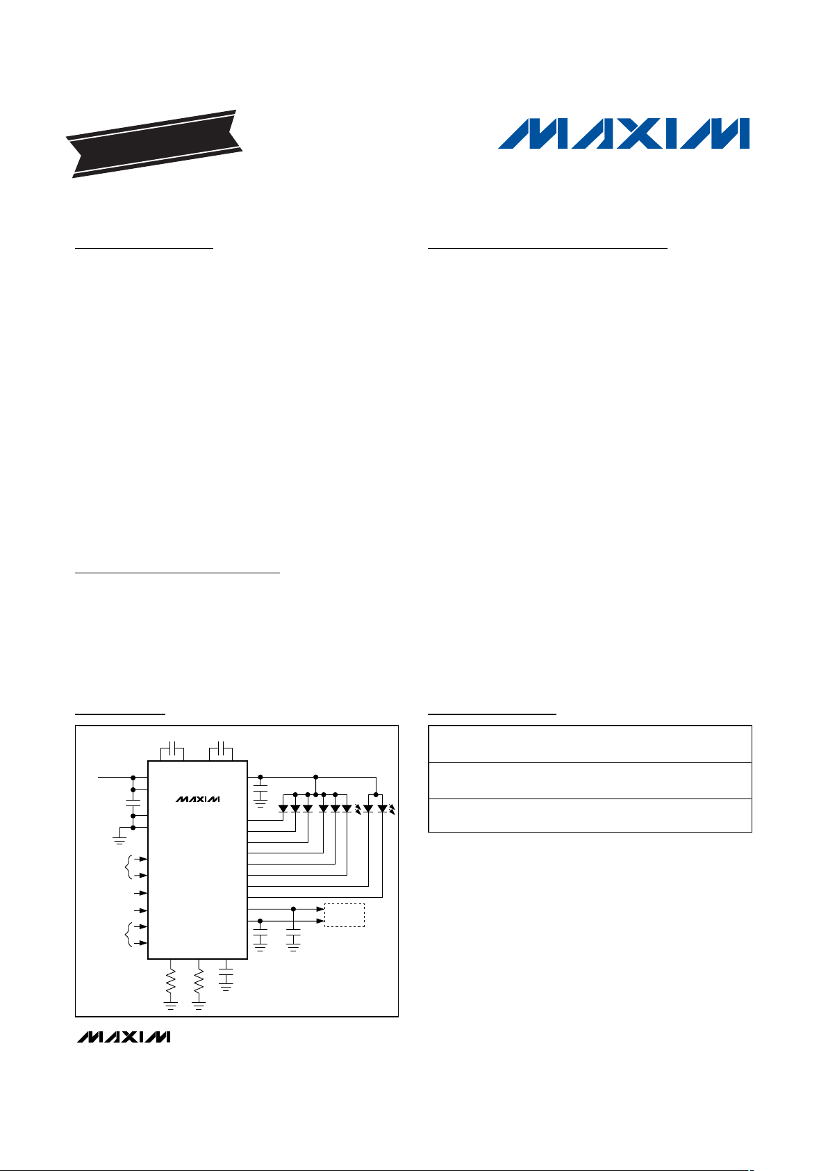
MAIN ON/OFF
AND DIMMING
MAX8645X
MAX8645Y
1μF
10μF
0.01μF
10μF
PIN
IN
PGND
GND
P1
P2
OUT
MAIN
FLASH
OUTPUT
UP TO 580mA
1μF1μF
LDO1
LDO2
C2P C2N
1μF
C1P C1N
REFSETM SETF
CAMERA
MODULE
DUAL-LDO
VOLTAGE
SELECTION
INPUT
2.7V TO 5.5V
ENM2
ENM1
ENF
ENLDO
M1
M2
M3
M4
M5
M6
F1
F2
FLASH ON/OFF
DUAL-LDO ON/OFF
Typical Operating Circuit
EP = Exposed paddle.
+Denotes a lead-free package.
Page 2
MAX8645X/MAX8645Y
1x/1.5x/2x White LED Charge Pumps with Two
LDOs in 4mm x 4mm TQFN
2 _______________________________________________________________________________________
ABSOLUTE MAXIMUM RATINGS
ELECTRICAL CHARACTERISTICS
(VIN= 3.6V, V
GND
= V
PGND
= 0V, ENM1 = ENM2 = ENF = IN, R
SETM
= R
SETF
= 6.8kΩ, P1 = P2 = unconnected, C
REF
= 0.01µF,
T
A
= -40°C to +85°C, unless otherwise noted. Typical values are at TA= +25°C.) (Note 1)
Stresses beyond those listed under “Absolute Maximum Ratings” may cause permanent damage to the device. These are stress ratings only, and functional
operation of the device at these or any other conditions beyond those indicated in the operational sections of the specifications is not implied. Exposure to
absolute maximum rating conditions for extended periods may affect device reliability.
PIN, IN, OUT, REFBP to GND................................-0.3V to +6.0V
SETF, SETM, ENLDO, ENM1, ENM2, ENF,
P1, P2, LDO1, LDO2 to GND....................-0.3V to (V
IN
+ 0.3V)
M1, M2, M3, M4, M5, M6, F1,
F2 to GND.............................................-0.3V to (V
OUT
+ 0.3V)
C1N, C2N to GND ......................................... -0.3V to (V
IN
+ 1V)
C1P, C2P
to GND........ -0.3V to the greater of (V
OUT
+ 1V) or (VIN+ 1V)
PGND to GND .......................................................-0.3V to +0.3V
OUT, LDO1, LDO2 Short Circuit to GND ...................Continuous
Continuous Power Dissipation (T
A
= +70°C)
28-Pin TQFN 4mm x 4mm
(derate 20.8mW/°C above +70°C).............................1666mW
Operating Temperature Range ...........................-40°C to +85°C
Junction Temperature......................................................+150°C
Storage Temperature Range .............................-65°C to +150°C
Lead Temperature (soldering, 10s) .................................+300°C
PARAMETER CONDITIONS MIN TYP MAX UNITS
IN Operating Voltage 2.7 5.5 V
Undervoltage-Lockout Threshold VIN rising or falling 2.25 2.45 2.60 V
Undervoltage-Lockout Hysteresis 130 mV
1MHz switching, no load, 1.5x or 2x mode 4.0 5.5
1x mode 10% setting, ENF = GND, V
ENLDO
= VIN,
I
LDO1
= I
LDO2
= 0A
0.4
mA
Supply Current
ENM1 = ENM2 = ENF = GND, V
ENLDO
= VIN,
I
LDO1
= I
LDO2
= 0A
110 µA
TA = +25°C 0.01 5
Shutdown Supply Current ENM1 = ENM2 = ENF = ENLDO = GND
T
A
= +85°C 0.1
µA
EN_ High Voltage VIN = 2.7V to 5.5V 1.4 V
EN_ Low Voltage V
IN
= 2.7V to 5.5V 0.4 V
TA = +25°C 0.01 1
EN_ Input Current V
EN_
= 0V or 5.5V
T
A
= +85°C 0.1
µA
ENM_ or ENF Low Shutdown
Delay t
SHDN
See Figure 1 1.5 2.0 2.5 ms
ENM_ or ENF t
LO
See Figure 1 0.5 250.0 µs
ENM_ or ENF t
HI
See Figure 1 0.5 µs
Initial ENM_ or ENF t
HI
Only required for first ENM_ or ENF pulse; see Figure 1 200 µs
P1, P2 Shutdown Input Current 1µA
P1, P2 Input Impedance 150 kΩ
Thermal-Shutdown Threshold Temperature rising +160 °C
Thermal-Shutdown Hysteresis 20 °C
CHARGE PUMP
Overvoltage-Protection Threshold V
OUT
rising 5 V
Soft-Start Time 2ms
Page 3
MAX8645X/MAX8645Y
1x/1.5x/2x White LED Charge Pumps with Two
LDOs in 4mm x 4mm TQFN
_______________________________________________________________________________________ 3
ELECTRICAL CHARACTERISTICS (continued)
(VIN= 3.6V, V
GND
= V
PGND
= 0V, ENM1 = ENM2 = ENF = IN, R
SETM
= R
SETF
= 6.8kΩ, P1 = P2 = unconnected, C
REF
= 0.01µF,
T
A
= -40°C to +85°C, unless otherwise noted. Typical values are at TA= +25°C.) (Note 1)
PARAMETER CONDITIONS MIN TYP MAX UNITS
1x to 1.5x or 1.5x to 2x Mode
Transition Threshold
90 100 110 mV
Input Voltage-Mode Transition
Hysteresis
150 mV
Charge-Pump Maximum OUT
Current
V
IN
≥ 3.15V, V
OUT
= 3.9V 580 mA
1x mode (VIN - V
OUT
) / I
OUT
0.3 1.0
1.5x mode (1.5VIN - V
OUT
) / I
OUT
1.1 4.0Open-Loop OUT Resistance
2x mode (2V
IN
- V
OUT
) / I
OUT
1.5 4.14
Ω
Charge-Pump Short-Circuit
Current
V
OUT
< 1.25V 500 mA
Switching Frequency 1 MHz
OUT Pulldown Resistance in
Shutdown
ENM_ = ENF = GND 5 kΩ
LED DRIVER
SET_ Bias Voltage TA = +25°C 0.6 V
TA = +25°C 0.01 1
SET_ Leakage in Shutdown ENM_ = ENF = GND
T
A
= +85°C 0.1
µA
SET_ Current Range 10 145 µA
SETM-to-Main LED Current Ratio
(I
M_
/I
SETM
)
100% setting, M1–M6 230 A/A
SETF-to-Flash LED Current Ratio
(I
F_/ISETF
)
100% setting, F1 and F2 1380 A/A
TA = +25°C -1.25 +1.25
M_, F_ Current Accuracy
T
A
= -40°C to current derating start temperature -4 +4
%
Maximum Main LED Sink Current R
SETM
= 4.6kΩ, for each M_ 30 mA
Maximum Flash LED Sink Current R
SETF
= 4.12kΩ, IF1 + I
F2
400 mA
Current-Derating-Function Start
Temperature
+40 °C
Current-Derating-Function Slope TA = +40°C to +85°C -1.7 %/°C
Dropout Voltage (Note 2) 40 90 mV
1.5x and 2x Regulation Voltage 150 mV
TA = +25°C 0.01 2
M_, F_ Leakage in Shutdown ENM_ = ENF = GND
T
A
= +85°C 0.1
µA
LDO_
Output Voltage Accuracy
I
LDO_
= 150mA, relative to V
OUT(NOM)
(Note 3) -1.7 0 +1.7 %
Output Current Range 0 200 mA
Current Limit V
LDO_
= 0V 280 475 750 mA
Soft-Start Current Limit 160 mA
Page 4
MAX8645X/MAX8645Y
1x/1.5x/2x White LED Charge Pumps with
Two LDOs in 4mm x 4mm TQFN
4 _______________________________________________________________________________________
ELECTRICAL CHARACTERISTICS (continued)
(VIN= 3.6V, V
GND
= V
PGND
= 0V, ENM1 = ENM2 = ENF = IN, R
SETM
= R
SETF
= 6.8kΩ, P1 = P2 = unconnected, C
REF
= 0.01µF,
T
A
= -40°C to +85°C, unless otherwise noted. Typical values are at TA= +25°C.) (Note 1)
PARAMETER CONDITIONS MIN TYP MAX UNITS
Soft-Start Done Time 100 µs
Dropout Voltage I
LDO_
= 200mA (Note 4) 120 320 mV
Load Regulation VIN = 3.7V, 100µA < I
LDO_
< 200mA 1.3 %
Power-Supply Rejection
ΔV
OUT
/ΔV
IN
10Hz to 10kHz, C
LDO_
= 1µF, I
LDO_
= 10µA -60 dB
Output Noise Voltage (RMS) 10Hz to 100kHz, C
LDO_
= 1µF, I
LDO_
= 10mA 40 µV
RMS
Note 1: All devices are 100% production tested at TA= +25°C. Limits over the operating temperature range are guaranteed by
design.
Note 2: LED dropout voltage is defined as the M_ or F_ to GND voltage at which current into M_ or F_ drops 10% from the value at
M_ or F_ = 0.2V.
Note 3: (Greater of 2.7V or (V
LDO_
+ 0.5V)) ≤ VIN≤ 5.5V.
Note 4: LDO dropout voltage is defined as V
IN
- V
OUT
when V
OUT
is 100mV below the value of V
OUT
measured when VIN=
V
OUT(NOM)
+ 1V. Since the minimum input voltage is 2.7V, this specification is only meaningful when V
OUT(NOM)
> 2.5V.
Typical Operating Characteristics
(VIN= V
EN_
= 3.6V, circuit of Figure 2, TA= +25°C, unless otherwise noted.)
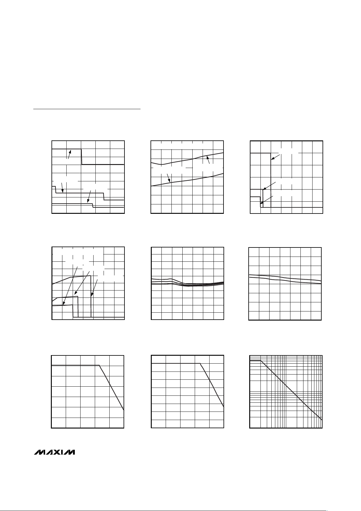
EFFICIENCY vs. Li+ BATTERY
VOLTAGE DRIVING SIX MAIN LEDs
MAX8645Y toc01
Li+ BATTERY VOLTAGE (V)
EFFICIENCY P
LED
/P
BATT
(%)
3.93.63.33.0
50
60
70
80
90
100
40
2.7 4.2
15mA/LED
4.5mA/LED
1.5mA/LED
EFFICIENCY vs. Li+ BATTERY
VOLTAGE DRIVING FLASH LED MODULE
MAX8645Y toc02
Li+ BATTERY VOLTAGE (V)
EFFICIENCY P
LED
/P
BATT
(%)
3.93.63.33.0
50
60
70
80
90
100
40
2.7 4.2
80mA TOTAL
160mA TOTAL
400mA TOTAL
BATTERY CURRENT vs. SUPPLY VOLTAGE
DRIVING SIX MAIN LEDs
MAX8645Y toc03
SUPPLY VOLTAGE (V)
BATTERY CURRENT (mA)
3.93.63.33.0
30
60
90
120
150
180
0
2.7 4.2
I
LED
= 15mA
I
LED
= 4.5mA
I
LED
= 1.5mA
V
IN
FALLING
V
IN
RISING
Page 5
MAX8645X/MAX8645Y
1x/1.5x/2x White LED Charge Pumps with
Two LDOs in 4mm x 4mm TQFN
_______________________________________________________________________________________ 5
BATTERY CURRENT vs. SUPPLY
VOLTAGE DRIVING FLASH
MAX8645Y toc04
SUPPLY VOLTAGE (V)
BATTERY CURRENT (mA)
3.93.63.33.0
100
200
300
400
500
600
700
800
900
0
2.7 4.2
I
FLASH
= 400mA
I
FLASH
= 160mA
I
FLASH
= 80mA
LDO GROUND-PIN SUPPLY
CURRENT vs. SUPPLY VOLTAGE
MAX8645Y toc05
SUPPLY VOLTAGE (V)
GROUND-PIN SUPPLY CURRENT (μA)
5.14.73.9 4.33.53.1
90
100
110
120
130
140
150
160
80
2.7 5.5
V
ENM_
= V
ENF
= 0V, V
ENLDO
= VIN
150mA, BOTH LDOs
NO LOAD, BOTH LDOs
INPUT RIPPLE VOLTAGE vs. SUPPLY
VOLTAGE WITH SIX MAIN LEDs
MAX8645Y toc06
SUPPLY VOLTAGE (V)
INPUT RIPPLE (mV
RMS
)
5.14.74.33.93.53.1
0.3
0.6
0.9
1.2
1.5
1.8
0
2.7 5.5
I
LED
= 15mA
I
LED
= 4.5mA
I
LED
= 1.5mA
INPUT RIPPLE VOLTAGE vs. SUPPLY
VOLTAGE WITH FLASH AND MAIN LEDs
MAX8645Y toc07
SUPPLY VOLTAGE (V)
INPUT RIPPLE (mV
RMS
)
5.14.73.1 3.5 3.9 4.3
1
2
3
4
5
7
9
6
8
10
0
2.7 5.5
FOUR MAIN LEDs AT 15mA EACH
I
FLASH
= 40mA
I
FLASH
= 160mA
I
FLASH
= 400mA
LED CURRENT MATCHING vs. SUPPLY
VOLTAGE WITH SIX MAIN LEDs
MAX8645Y toc08
SUPPLY VOLTAGE (V)
MAIN LED CURRENT (mA)
5.14.73.9 4.33.53.1
14.2
14.4
14.6
14.8
15.0
15.2
15.4
15.6
15.8
16.0
14.0
2.7 5.5
LED CURRENT MATCHING vs. SUPPLY
VOLTAGE WITH TWO FLASH LEDs
MAX8645Y toc09
SUPPLY VOLTAGE (V)
FLASH LED CURRENT (mA)
5.14.74.33.93.53.1
99.0
98.5
99.5
100.0
100.5
101.0
101.5
102.0
98.0
2.7 5.5
LED CURRENT vs. AMBIENT
TEMPERATURE WITH SIX MAIN LEDs
MAX8645Y toc10
TA (°C)
TOTAL LED CURRENT (mA)
603510-15
15
30
45
60
75
90
105
0
-40 85
LED CURRENT vs. AMBIENT
TEMPERATURE WITH FLASH
MAX8645Y toc11
TA (°C)
TOTAL LED CURRENT (mA)
603510-15
50
100
150
200
250
300
350
400
450
0
-40 85
INDIVIDUAL MAIN LED CURRENT
vs. R
SETM
MAX8645Y toc12
R
SETM
(kΩ)
MAIN LED CURRENT (mA)
10
10
100
1
1001
Typical Operating Characteristics (continued)
(VIN= V
EN_
= 3.6V, circuit of Figure 2, TA= +25°C, unless otherwise noted.)
Page 6

MAX8645X/MAX8645Y
1x/1.5x/2x White LED Charge Pumps with Two
LDOs in 4mm x 4mm TQFN
6 _______________________________________________________________________________________
INDIVIDUAL FLASH LED CURRENT
vs. R
SETF
MAX8645Y toc13
R
SETF
(kΩ)
FLASH LED CURRENT (mA)
10
20
200
2000
2
1100
OPERATING WAVEFORMS (1x MODE)
MAX8645Y toc14
50mV/div
AC-COUPLED
20mV/div
AC-COUPLED
2mA/div
AC-COUPLED
V
OUT
V
IN
I
IN
400ns/div
6 MAIN LEDS AT 20mA EACH
OPERATING WAVEFORMS (1.5x MODE)
MAX8645Y toc15
50mV/div
AC-COUPLED
20mV/div
AC-COUPLED
2mA/div
AC-COUPLED
V
OUT
V
IN
I
IN
400ns/div
6 MAIN LEDS AT 20mA EACH
OPERATING WAVEFORMS (2x MODE)
MAX8645Y toc16
50mV/div
AC-COUPLED
20mV/div
AC-COUPLED
2mA/div
AC-COUPLED
V
OUT
V
IN
I
IN
400ns/div
6 MAIN LEDS AT 20mA EACH,
FLASH AT 400mA TOTAL
STARTUP AND SHUTDOWN
MAIN LED RESPONSE
MAX8645Y toc17
5V/div
0V
100mA/div
5V/div
0V
0A
V
ENM_
I
OUT
V
OUT
1ms/div
6 MAIN LEDS AT 20mA EACH
STARTUP AND SHUTDOWN
FLASH LED RESPONSE
MAX8645Y toc18
5V/div
0V
500mA/div
500mA/div
5V/div
0V
0A
0A
V
ENF
I
IN
V
OUT
I
OUT
1ms/div
6 MAIN LEDS AT 20mA EACH,
400mA TOTAL FLASH
Typical Operating Characteristics (continued)
(VIN= V
EN_
= 3.6V, circuit of Figure 2, TA= +25°C, unless otherwise noted.)
Page 7

MAX8645X/MAX8645Y
1x/1.5x/2x White LED Charge Pumps with Two
LDOs in 4mm x 4mm TQFN
_______________________________________________________________________________________ 7
SINGLE-WIRE DIMMING RESPONSE
MAX8645Y toc19
5V/div
0V
500mA/div
2V/div
0A
0V
V
ENM1,
V
ENM2
I
OUT
V
OUT
10ms/div
LDO DROPOUT VOLTAGE
vs. OUTPUT CURRENT
MAX8645Y toc20
OUTPUT CURRENT (mA)
DROPOUT VOLTAGE (mV)
15010050
20
40
60
80
100
120
140
0
0200
LDO OUTPUT VOLTAGE
ACCURACY vs. OUTPUT CURRENT
MAX8645Y toc21
OUTPUT CURRENT (mA)
OUTPUT VOLTAGE ACCURACY (%)
15010050
-0.8
-0.6
-0.4
-0.2
0
0.2
0.4
0.6
0.8
1.0
-1.0
0200
LOAD-TRANSIENT RESPONSE
MAX8645Y toc22
50mV/div
AC-COUPLED
100mA
1mA
V
LDO_
I
LDO_
10μs/div
V
LDO_
= 2.6V
LOAD-TRANSIENT RESPONSE
NEAR DROPOUT
MAX8645Y toc23
50mV/div
AC-COUPLED
100mA
1mA
V
LDO_
I
LDO_
10μs/div
VIN - V
OUT
= 77mV, V
LDO_
= 2.6V
Typical Operating Characteristics (continued)
(VIN= V
EN_
= 3.6V, circuit of Figure 2, TA= +25°C, unless otherwise noted.)
Page 8

MAX8645X/MAX8645Y
1x/1.5x/2x White LED Charge Pumps with Two
LDOs in 4mm x 4mm TQFN
8 _______________________________________________________________________________________
Pin Description
PIN NAME FUNCTION
1 PIN
Supply Voltage Input. Bypass to PGND with a 10µF ceramic capacitor. The input voltage range is
2.7V to 5.5V. PIN is high impedance during shutdown.
2IN
Chip Supply Voltage Input. Bypass to GND with a 10µF ceramic capacitor as close as possible to the
IC. The input voltage range is 2.7V to 5.5V. IN is high impedance during shutdown.
3 GND G r ound . C onnect G N D to system g r ound and the i np ut b yp ass cap aci tor as cl ose as p ossi b l e to the IC .
4 LDO1
LDO1 Output. Bypass with a 1µF ceramic capacitor to GND. LDO1 is pulled to ground through an
internal 400kΩ resistor during shutdown.
5 LDO2
LDO2 Output. Bypass with a 1µF ceramic capacitor to GND. LDO2 is pulled to ground through an
internal 400kΩ resistor during shutdown.
6 REFBP Reference Filter. Bypass REFBP with a 0.01µF ceramic capacitor to GND.
7 SETF
Bias Current Set Input for F1, F2. The current flowing out of SETF sets the maximum (100%) bias
current into each LED. V
SETF
is internally biased to 0.6V. Connect a resistor (R
SETF
) from SETF to
GND to set the flash current. R
SETF
= 82.8 / I
LED(MAX)
. SETF is high impedance during shutdown.
8 SETM
Bi as C ur r ent S et Inp ut for M 1–M 4. The cur r ent fl ow i ng out of S E TM sets the m axi m um ( 100%) b i as
cur r ent i nto each LE D . V
S E T M
i s i nter nal l y b i ased to 0.6V . C onnect a r esi stor ( R
S E T M
) fr om S E TM to GN D
to set the m ai n LE D cur r ent. R
S E T M
= 138 / I
L E D ( M AX )
. S E TM i s hi g h i m p ed ance d ur i ng shut d ow n.
9, 10 F2, F1
400m A C om b i ned - C ur r ent Fl ash LE D C athod e C onnecti on and C har g e- P um p Feed b ack. C ur r ent fl ow i ng
i nto F_ i s b ased on I
S E T F
. The char g e p um p r eg ul ates the l ow est F_ vol tag e to 0.15V . Gr ound i ng any F_
i np ut for ces OU T to op er ate at ap p r oxi m atel y 5V . C onnect F_ to OU T i f thi s LE D i s not p op ul ated .
11–16 M6–M1
30mA M ai n LE D Cathod e Connecti on and C har g e- P ump Feed b ack. C ur rent fl owi ng i nto M _ i s based on the
E N _ confi g ur ation and I
S E TM
. The char ge p um p reg ulates the l owest M _ inp ut voltag e to 0.15V . Gr ound i ng
any M _ for ces OU T to oper ate at ap pr oxim atel y 5V . Connect M_ to OU T i f thi s L E D i s not p op ul ated .
17 P2
Default Output-Voltage Select Input. P1 and P2 set the LDO1 and LDO2 voltages to one of nine
combinations (Table 2). P2 is high impedance in an off condition and shortly after an on condition.
18 ENLDO
LDO Output Enable. Drive to a logic-level high to turn on both LDOs. Drive to a logic-level low to turn
off both LDOs.
19 ENM2
Enable and Dimming Control for M1–M6. Drive both ENM1 and ENM2 to a logic-level high to turn on
the main LEDs. Drive both ENM1 and ENM2 to a logic-level low to turn off the main LEDs. Alternate
dimming techniques are discussed in the Applications Information section.
20 ENM1
Enable and Dimming Control for M1–M6. Drive both ENM1 and ENM2 to a logic-level high to turn on
the main LEDs. Drive both ENM1 and ENM2 to a logic-level low to turn off the main LEDs. Alternate
dimming techniques are discussed in the Applications Information section.
21 ENF
Enable and Dimming Control for F1, F2. Drive ENF to a logic-level high to turn on the flash LEDs.
Drive ENF to a logic-level low to turn off the flash LEDs. Dimming techniques are discussed in the
Applications Information section.
22 C1N
Transfer Capacitor 1 Negative Connection. Connect a 1µF ceramic capacitor between C1P and C1N.
C1N is internally shorted to IN during shutdown.
Page 9

MAX8645X/MAX8645Y
1x/1.5x/2x White LED Charge Pumps with Two
LDOs in 4mm x 4mm TQFN
_______________________________________________________________________________________ 9
Detailed Description
The MAX8645X/MAX8645Y charge pumps drive up to
six white LEDs in the main display for backlighting and
up to two white LEDs for flash, all with regulated constant current for uniform intensity. By utilizing adaptive
1x/1.5x/2x charge-pump modes and very-low-dropout
current regulators, they achieve high efficiency over the
1-cell lithium-battery input voltage range. 1MHz fixedfrequency switching allows for tiny external components and low input ripple. Two on-board 200mA
programmable-output-voltage LDOs are provided to
meet camera-module requirements.
1x to 1.5x Switchover
When VINis higher than V
OUT
, the MAX8645X/
MAX8645Y operate in 1x mode and V
OUT
is pulled up
to VIN. The internal current regulators regulate the LED
current. As VINdrops, VM_(or VF_) eventually falls
below the switchover threshold of 100mV and the
MAX8645X/MAX8645Y start switching in 1.5x mode.
When the input voltage rises above V
OUT
by approximately 50mV, the MAX8645X/MAX8645Y switch back to
1x mode.
1.5x to 2x Switchover
When VINis less than V
OUT
but greater than 2/3 V
OUT
,
the MAX8645X/MAX8645Y operate in 1.5x mode. The
internal current regulators regulate the LED current. As
VINdrops, VM_(or VF_) eventually falls below the
switchover threshold of 100mV, and the MAX8645X/
MAX8645Y start switching in 2x mode. When the input
voltage rises above 2/3 V
OUT
by approximately 50mV,
the MAX8645X/MAX8645Y switch back to 1.5x mode.
Soft-Start
The MAX8645X/MAX8645Y include soft-start circuitry to
limit inrush current at turn-on. Once the input voltage is
applied, the output capacitor is charged directly from
the input with a ramped current source (with no chargepump action) until the output voltage approaches the
input voltage. Once the output capacitor is charged,
the charge pump determines if 1x, 1.5x, or 2x mode is
required. In the case of 1x mode, the soft-start is terminated and normal operation begins. In the case of 1.5x
or 2x mode, soft-start operates until the lowest voltage
of M1–M6 and F1, F2 reaches regulation. If the output
is shorted to ground or is pulled to less than 1.25V, the
output current is limited by soft-start.
True Shutdown™ Mode
When ENM1, ENM2, and ENF are simultaneously held
low for 2ms or longer, the MAX8645X/MAX8645Y are
shut down and put in a low-current shutdown mode,
and the input is isolated from the output. OUT is internally pulled to GND with 5kΩ during shutdown.
Thermal Derating
The MAX8645X/MAX8645Y limit the maximum LED current depending on the die temperature. The maximum
LED current is set by the R
SETM
and R
SETF
resistors.
Once the temperature reaches +40°C, the LED current
decreases by 1.7%/°C. Due to the package’s exposed
paddle, the die temperature is always very close to the
PCB temperature.
The temperature derating function allows the LED current to be safely set higher at normal operating temperatures, thereby allowing either a brighter display or
fewer LEDs to be used for normal display brightness.
Pin Description (continued)
PIN NAME FUNCTION
23 C1P
Transfer Capacitor 1 Positive Connection. Connect a 1µF ceramic capacitor between C1P and C1N.
During shutdown, if OUT > IN, C1P is shorted to OUT. If OUT < IN, C1P is shorted to IN.
24 PGND Power Ground. Connect PGND to system ground. PGND is used for charge-pump switching currents.
25 OUT
Charge-Pump Output. Bypass OUT to GND with a 10µF ceramic capacitor. Connect to the anodes of
all the LEDs. OUT is internally pulled to ground through a 5kΩ resistor during
shutdown.
26 C2P
Transfer Capacitor 2 Positive Connection. Connect a 1µF ceramic capacitor between C2P and C2N.
During shutdown, if OUT > IN, C2P is shorted to OUT. If OUT < IN, C2P is shorted to IN.
27 C2N
Transfer Capacitor 2 Negative Connection. Connect a 1µF ceramic capacitor between C2P and C2N.
C2N is internally shorted to IN during shutdown.
28 P1
Default Output-Voltage Select Input. P1 and P2 set the LDO1 and LDO2 voltages to one of nine
combinations (Table 2). P1 is high impedance in an off condition and shortly after in an on condition.
— EP Exposed Paddle. Connect to GND and PGND.
True Shutdown is a trademark of Maxim Integrated Products, Inc.
Page 10

MAX8645X/MAX8645Y
1x/1.5x/2x White LED Charge Pumps with Two
LDOs in 4mm x 4mm TQFN
10 ______________________________________________________________________________________
Thermal Shutdown
The MAX8645X/MAX8645Y include a thermal-limit circuit
that shuts down the IC at approximately +160°C. Turnon occurs after the IC cools by approximately 20°C.
Applications Information
Setting the Main Output Current
SETM controls M1–M6 regulation current. Current flowing into M1, M2, M3, M4, M5, and M6 is a multiple of
the current flowing out of SETM:
IM1= IM2= IM3= IM4= IM5= IM6= K x (0.6V / R
SETM
)
where K = 23, 69, or 230 (depending upon the state of
ENM1 and ENM2; see Table 1), and R
SETM
is the resistor connected between SETM and GND (see the
Typical Operating Circuit).
Setting the Flash Output Current
SETF controls the F1, F2 regulation current. Current
flowing into F1 and F2 is a multiple of the current flowing out of SETF:
IF1= IF2= N x (0.6V / R
SETF
)
where N = 1380.
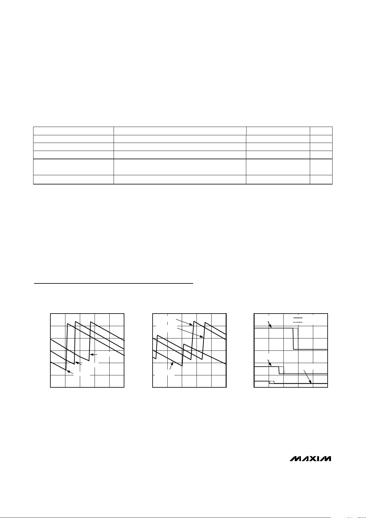
Single-Wire Pulse Dimming
For more dimming flexibility or to reduce the number of
control traces, the MAX8645X/MAX8645Y support serial
pulse dimming. Connect ENM1 and ENM2 together to
enable single-wire pulse dimming of the main LEDs (or
ENF only for single-wire pulse dimming of the flash
LEDs). When ENM1 and ENM2 (or ENF) go high
simultaneously, the main (or flash) LEDs are enabled at
full brightness. Each subsequent low-going pulse
(500ns to 250µs pulse width) reduces the LED current
by 3.125% (1/32), so after one pulse, the LED current is
96.9% (or 31/32) x I
LED
. The 31st pulse reduces the
current to 0.03125 x I
LED
. The 32nd pulse sets the LED
current back to I
LED
. Figure 1 shows a timing diagram
for single-wire pulse dimming. Because soft-start is
longer than the initial tHI, apply dimming pulses quickly
upon startup (after initial tHI) to avoid LED current transitioning through full brightness.
Simple On/Off Control
If dimming control is not required, connect ENM1 to
ENM2 for simple on/off control. Drive both ENM1 and
ENM2 to a logic-level high to turn on the main LEDs.
Drive both ENM1 and ENM2 to a logic-level low to turn
off the main LEDs. ENF is the simple on/off control for
the flash LEDs. Drive ENF to a logic-level high to turn
on the flash LEDs. Drive ENF to a logic-level low to turn
off the flash LEDs. In this case, LED current is set by
the values of R
SETM
and R
SETF
.
Dimming Using PWM into ENM1
Use ENM2 for shutdown and drive ENM1 with a PWM
signal. LED brightness can be varied from 10% to full
brightness based upon the duty cycle of the PWM signal. Drive ENM2 high to keep the IC on, eliminating any
soft-start delay that would impede PWM control and
allowing a PWM frequency up to 5kHz (Figure 2).
Driving Fewer than Eight LEDs
When driving fewer than eight LEDs, two connection
schemes can be used. The first scheme is shown in
Figure 3 where LED drivers are connected together.
This method allows increased current through the LED
and effectively allows total LED current to be I
LED
multiplied by the number of connected drivers. The second
method of connection is shown in Figure 4 where standard white LEDs are used and fewer than eight are
connected. This scheme does not alter current through
each LED but ensures that the unused LED driver is
properly disabled.
10243 5 27 28 29 30 31 32
SHUTDOWN
t
SHDN
2ms (typ)
2/32
1/32
3/32
4/32
5/32
27/32
28/32
29/32
30/32
31/32
31/32
32/32
32/32
SHUTDOWN
I
M_
OR I
F_
ENM1 AND ENM2
OR
ENF
t
SOFT-START
INITIAL t
HI
t
LO
t
HI
≥ 200μs
≥ 500ns
500ns TO 250μs
Figure 1. ENM_ and ENF Timing Diagram
ENM1/ENM2 STATES BRIGHTNESS
M1–M6
CURRENT
ENM1 = low, ENM2 = low Shutdown 0
ENM1 = low, ENM2 = high 1/10 brightness 23 x I
SETM
ENM1 = high, ENM2 = low 3/10 brightness 69 x I
SETM
ENM1 = high, ENM2 = high Full brightness 230 x I
SETM
Table 1. ENM1/ENM2 States
Page 11

MAX8645X/MAX8645Y
1x/1.5x/2x White LED Charge Pumps with Two
LDOs in 4mm x 4mm TQFN
______________________________________________________________________________________ 11
MAX8645X
MAX8645Y
1μF
10μF
0.01μF
10μF
PIN
IN
GND
P1
P2
OUT
MAIN FLASH
OUTPUT
UP TO 480mA
1μF
1μF
LDO1
LDO2
C2P C2N
1μF
C1P C1N
REFBPSETM SETF PGND
ON/OFF AND
VOLTAGE
SELECTION
INPUT
2.7V TO 5.5V
ENM2
ENM1
ENF
ENLDO
M1
M2
M3
M4
M5
M6
F1
F2
4.12kΩ
6.81kΩ
Figure 3. Providing Increased LED Current per LED
MAX8645X
MAX8645Y
C4
1μF
C8
0.01μF
C1
10μF
PIN
IN
ON
OFF
GND
P1
P2
OUT
MAIN FLASH
OUTPUT
UP TO 480mA
C6
1μF
C7
1μF
C5
10μF
LDO1
LDO2
C2P C2N
C3
1μF
C1P C1N
REFBPSETM SETF PGND
VOLTAGE
SELECTION
INPUT
2.7V TO 5.5V
ENM2
ENM1
ENF
ENLDO
M1
M2
M3
M4
M5
M6
F1
F2
R
SETF
4.12kΩ
PWM INPUT
ON/OFF
ON/OFF
R
SETM
6.81kΩ
Figure 2. Dimming Using PWM Signal into ENM1
Page 12

MAX8645X/MAX8645Y
1x/1.5x/2x White LED Charge Pumps with Two
LDOs in 4mm x 4mm TQFN
12 ______________________________________________________________________________________
Input Ripple
For LED drivers, input ripple is more important than output ripple. Input ripple is highly dependent on the
source supply’s impedance. Adding a lowpass filter to
the input further reduces input ripple. Alternately,
increasing CINto 22µF cuts input ripple in half with only
a small increase in footprint. The 1x mode always has
very low input ripple.
Typical operating waveforms shown in the Typical
Operating Characteristics show input ripple current in
1x, 1.5x, and 2x modes.
LDO Output Voltage Selection (P1 and P2)
As shown in Table 2, the LDO output voltages, LDO1
and LDO2 are pin programmable by the logic states of
P1 and P2. P1 and P2 are tri-level inputs: IN, open, and
GND. The input voltage, VIN, must be greater than the
selected LDO1 and LDO2 voltages. The logic states of
P1 and P2 can be programmed only during ENLDO
low. Once the LDO_ voltages are programmed, their
values do not change by changing P1 or P2 during
ENLDO high.
Component Selection
Use only ceramic capacitors with an X5R, X7R, or better
dielectric. See Table 3 for a list of recommended parts.
Connect a 1µF ceramic capacitor between LDO1 and
GND, and a second 1µF ceramic capacitor between
LDO2 and GND for 200mA applications. The LDO output capacitor’s (C
LDO
) equivalent series resistance
(ESR) affects stability and output noise. Use output
capacitors with an ESR of 0.1Ω or less to ensure stability
and optimum transient response. Connect C
LDO_
as
close as possible to the MAX8645X/MAX8645Y to minimize the impact of PCB trace inductance.
MAX8645X
MAX8645Y
1μF
10μF
0.01μF
10μF
PIN
IN
GND
P1
P2
OUT
MAIN FLASH
OUTPUT
UP TO 240mA
1μF
1μF
LDO1
LDO2
C2P C2N
1μF
C1P C1N
REFBPSETM SETF PGND
ON/OFF AND
VOLTAGE
SELECTION
INPUT
2.7V TO 5.5V
ENM2
ENM1
ENF
ENLDO
M1
M2
M3
M4
M5
M6
F1
F2
4.12kΩ
6.81kΩ
Figure 4. Schematic for When Fewer than 8 LEDs Are Acceptable
MAX8645X MAX8645Y
P1 P2
LDO1 (V) LDO2 (V)
LDO1 (V) LDO2 (V)
IN IN 3.3 1.8 2.8 2.6
IN OPEN 3.0 1.5 2.8 2.8
IN GND 2.8 1.5 2.9 1.5
OPEN IN 3.3 1.5 2.6 1.9
OPEN OPEN 2.6 1.8 2.6 2.6
OPEN GND 2.6 1.5 2.8 1.9
GND IN 3.0 1.8 2.9 1.8
GND OPEN 2.8 1.8 2.9 1.9
GND GND 2.5 1.8 2.9 2.9
Table 2. P1 and P2, LDO Output Voltage
Selection
Page 13

MAX8645X/MAX8645Y
1x/1.5x/2x White LED Charge Pump with
Two LDOs in 4mm x 4mm TQFN
______________________________________________________________________________________ 13
MAX8645YETI
PCB Layout and Routing
The MAX8645X/MAX8645Y are high-frequency,
switched-capacitor voltage regulators. For best circuit
performance, use a solid ground plane and place CIN,
C
OUT
, C3, and C4 as close as possible to the IC. There
should be no vias on CIN. Connect GND and PGND to
the exposed paddle directly under the IC. Refer to the
MAX8645Y evaluation kit for an example.
DESIGNATION VALUE MANUFACTURER PART DESCRIPTION
C1, C5 10µF TDK C2012X5R0J106M 10µF ±20%, 6.3V X5R ceramic capacitors (0805)
C3, C4, C6, C7 1µF TDK C1005X5R0J105M 1µF ±20%, 6.3V X5R ceramic capacitors (0402)
C8 0.01µF TDK C1005X7R1E103K 0.01µF ±10%, 25V X7R ceramic capacitor (0402)
D1–D4 — Nichia NSCW215T White LEDs
D5 (D5–D8) — Nichia NBCW011T White LEDs, 4 LEDs in one package
Panasonic
R
SETM
, R
SETF
As
required
Vishay
— 1% resistors
Table 3. Recommended Components for Figure 2
Chip Information
PROCESS: BiCMOS
9
8
11
12
13
14
10
23
22
25
26
27
28
24
21 20 19 18 17 16 15
1234567
MAX8645X
MAX8645Y
THIN QFN
(4mm x 4mm, 0.4mm LEAD PITCH)
TOP VIEW
PGND
C1P
ENF
ENM2
P2
M1
M2
M3
M4
M5
M6
F1
F2
SETM
REFBP
LDO2
LDO1
GND
IN
PIN
ENM1
ENLDO
C2P
C1N
C2N
+ DENOTES A LEAD-FREE PACKAGE.
OUT
P1
SETF
Pin Configuration
Page 14

MAX8645X/MAX8645Y
1x/1.5x/2x White LED Charge Pumps with
Two LDOs in 4mm x 4mm Thin QFN
14 ______________________________________________________________________________________
Package Information
(The package drawing(s) in this data sheet may not reflect the most current specifications. For the latest package outline information
go to www.maxim-ic.com/packages
.)
24L QFN THIN.EPS
PACKAGE OUTLINE,
21-0139
2
1
E
12, 16, 20, 24, 28L THIN QFN, 4x4x0.8mm
Page 15

MAX8645X/MAX8645Y
1x/1.5x/2x White LED Charge Pumps with Two
LDOs in 4mm x 4mm TQFN
Maxim cannot assume responsibility for use of any circuitry other than circuitry entirely embodied in a Maxim product. No circuit patent licenses are
implied. Maxim reserves the right to change the circuitry and specifications without notice at any time.
15 ____________________Maxim Integrated Products, 120 San Gabriel Drive, Sunnyvale, CA 94086 408-737-7600
© 2006 Maxim Integrated Products is a registered trademark of Maxim Integrated Products, Inc.
Package Information (continued)
(The package drawing(s) in this data sheet may not reflect the most current specifications. For the latest package outline information
go to www.maxim-ic.com/packages
.)
PACKAGE OUTLINE,
21-0139
2
2
E
12, 16, 20, 24, 28L THIN QFN, 4x4x0.8mm
 Loading...