

Page 1
19-0239; Rev 3; 8/13
MAX860/MAX861
50mA, Frequency-Selectable,
Switched-Capacitor Voltage Converters
For pricing, delivery, and ordering information, please contact Maxim Direct
at 1-888-629-4642, or visit Maxim’s website at www.maximintegrated.com.
_______________General Description
The MAX860/MAX861 charge-pump voltage converters
invert input voltages ranging from +1.5V to +5.5V, or
double input voltages ranging from +2.5V to +5.5V.
Because of their high switching frequencies, these
devices use only two small, low-cost capacitors. Their
50mA output makes switching regulators unnecessary,
eliminating inductors and their associated cost, size,
and EMI. Greater than 90% efficiency over most of the
load-current range, combined with a typical operating
current of only 200µA (MAX860), provides ideal performance for both battery-powered and board-level voltage-conversion applications.
A frequency-control (FC) pin provides three switchingfrequencies to optimize capacitor size and quiescent
current and to prevent interference with sensitive circuitry. Each device has a unique set of three available
frequencies. A shutdown (S—H—D—N–) pin reduces current
consumption to less than 1µA. The MAX860/MAX861
are suitable for use in applications where the ICL7660
and MAX660's switching frequencies are too low. The
MAX860/MAX861 are available in 8-pin µMAX
®
and
SO packages.
________________________Applications
Portable Computers
Medical Instruments
Interface Power Supplies
Hand-Held Instruments
Operational-Amplifier Power Supplies
____________________________Features
o 8-Pin, 1.11mm High µMAX Package
o Invert or Double the Input Supply Voltage
o Three Selectable Switching Frequencies
o High Frequency Reduces Capacitor Size
o 87% Efficiency at 50mA
o 200µA Quiescent Current (MAX860)
o 1µA Shutdown Supply Current
o 600mV Voltage Drop at 50mA Load
o 12Ω Output Resistance
______________Ordering Information
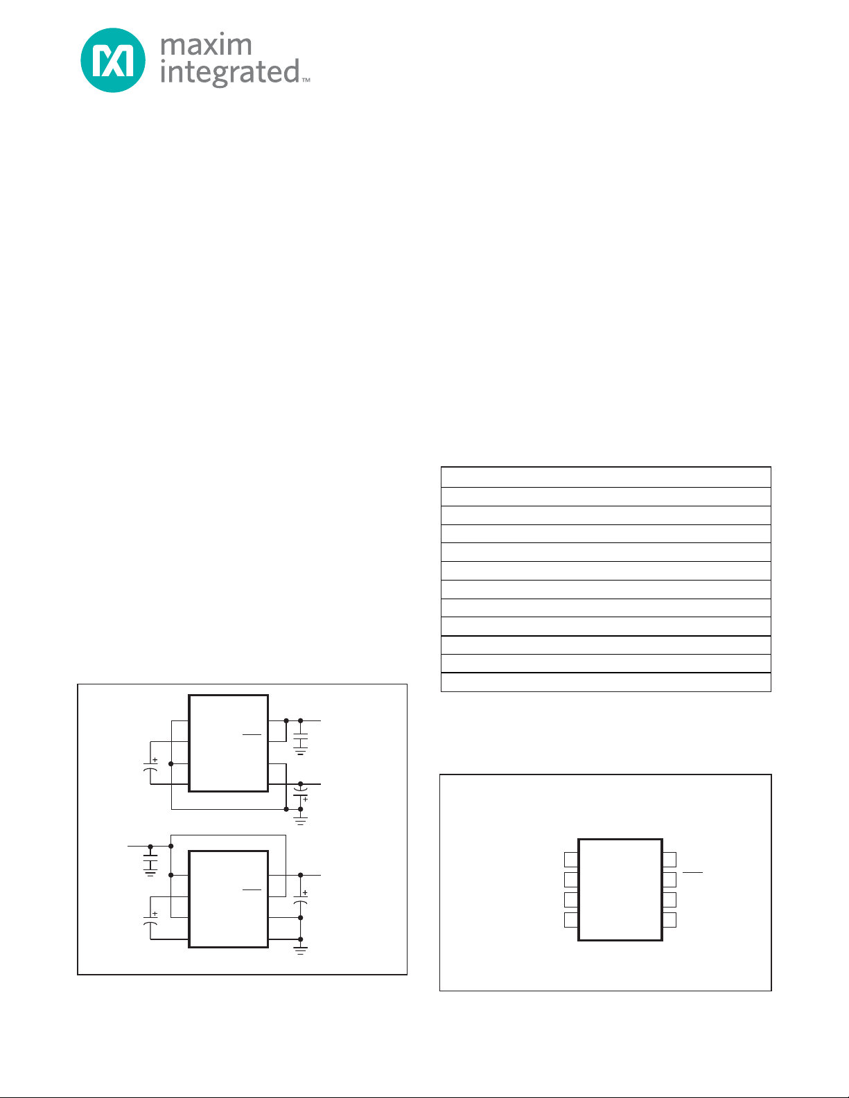
__________________Pin Configuration
PART TEMP RANGE PIN-PACKAGE
MAX860ISA -25°C to +85°C 8 SO
MAX860IUA -25°C to +85°C 8 µMAX
MAX860C/D 0°C to +70°C Dice*
MAX860ESA -40°C to +85°C 8 SO
MAX860MJA -55°C to +125°C 8 CERDIP†
-55°C to +125°C 8 SO
MAX861ISA -25°C to +85°C 8 SO
MAX861IUA -25°C to +85°C 8 µMAX
MAX861C/D 0°C to +70°C Dice*
MAX861ESA -40°C to +85°C 8 SO
MAX861MJA -55°C to +125°C 8 CERDIP†
__________Typical Operating Circuit
*
Dice are tested at TA= +25°C, DC parameters only.
†
Contact factory for availability.
µMAX is a registered trademark of Maxim Integrated Products, Inc.
MAX860MSA/PR3
1
MAX860
FC
MAX861
2
C1+
3
GND
4
10μF
C1
INPUT
VOLTAGE
+2.5V TO +5.5V
C1
C1- OUT
VOLTAGE INVERTER
1
MAX860
FC
MAX861
2
C1+
3
GND
4
10μF
C1- OUT
POSITIVE VOLTAGE DOUBLER
V
SHDN
V
SHDN
8
DD
7
6
LV
5
8
DD
7
6
LV
5
INPUT
VOLTAGE
+1.5V TO +5.5V
INVERTED
NEGATIVE
OUTPUT
10μF
C2
DOUBLED
POSITIVE
OUTPUT
10μF
C2
TOP VIEW
C1+
GND
C1-
+
FC
1
MAX860
2
MAX861
3
4
SO/μMAX
V
8
DD
SHDN
7
LV
6
OUT
5
Page 2
MAX860/MAX861
50mA, Frequency-Selectable,
Switched-Capacitor Voltage Converters
2
Maxim Integrated
ABSOLUTE MAXIMUM RATINGS
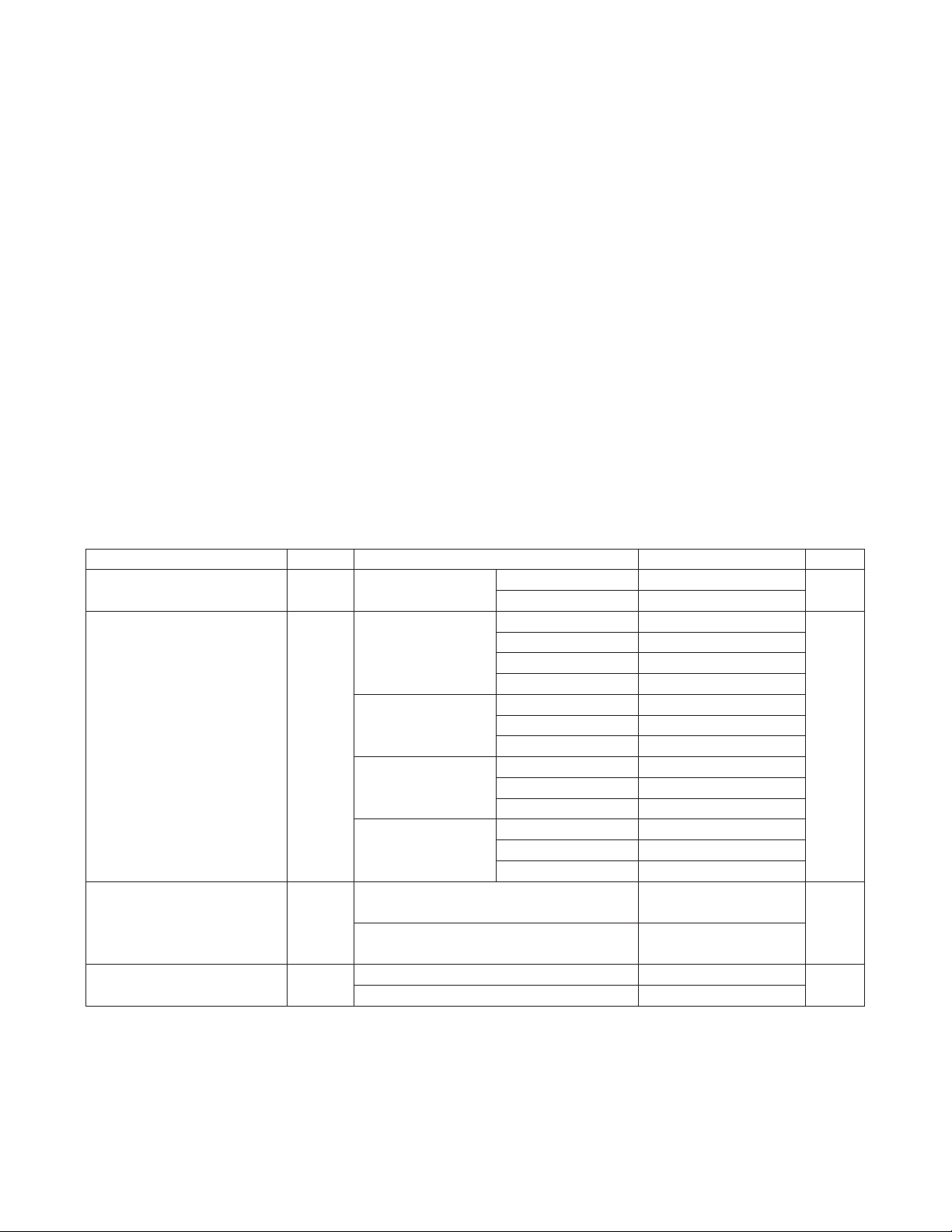
ELECTRICAL CHARACTERISTICS
(Typical Operating Circuit (Inverter), VDD= +5V, –S—H—D—N–= VDD, FC = LV = GND, C1 = C2 = 10µF (Note 2), TA= T
MIN
to T
MAX
, unless
otherwise noted. Typical values are at T
A
= +25°C.)
Stresses beyond those listed under “Absolute Maximum Ratings” may cause permanent damage to the device. These are stress ratings only, and functional
operation of the device at these or any other conditions beyond those indicated in the operational sections of the specifications is not implied. Exposure to
absolute maximum rating conditions for extended periods may affect device reliability.
Supply Voltage (VDDto GND or GND to OUT) ...................+6.0V
Input Voltage Range (LV, FC, –S—H—D—N–) ...................(OUT - 0.3V)
to (V
DD
+ 0.3V)
Continuous Output Current (OUT, V
DD
) .............................60mA
Output Short-Circuit to GND (Note 1).......................................1s
Continuous Power Dissipation (T
A
= +70°C)
SO (derate 5.88mW/°C above +70°C).........................471mW
µMAX (derate 4.2mW/°C above +70°C) ......................362mW
CERDIP (derate 8.00mW/°C above +70°C).................640mW
Operating Temperature Ranges
MAX86_I_A ......................................................-25°C to +85°C
MAX86_ESA.....................................................-40°C to +85°C
MAX86_M_A ..................................................-55°C to +125°C
Storage Temperature Range .............................-65°C to +160°C
Lead Temperature (soldering, 10s) .................................+300°C
Soldering Temperature (reflow) .......................................+240°C
I
L
= 10mA, VDD= 2V
RL= 1kΩ
IL= 50mA
VDD= 3V, V
OUT
more negative than -2.5V
VDD= 5V, V
OUT
more negative than -3.75V
MAX861M
MAX860M
MAX861I/E
MAX860I/E
CONDITIONS
Ω
20 35
R
OUT
Output Resistance
(Note 4)
12 25
mAI
OUT
Output Current
50 100
mA
6.5
I
DD
No-Load Supply Current
(Note 3)
2.6
0.5
2.5 5.0
1.1 2.0
V
2.5 5.5
V
DD
Supply Voltage
1.5 5.5
0.3 0.4
3.3
1.3
0.4
0.2 0.3
0.07
0.6 1.0
1.4 2.5
UNITSMIN TYP MAXSYMBOLPARAMETER
Inverter, LV = GND
Doubler, LV = OUT
FC = VDD= 5V
FC = OUT
FC = GND
FC = VDD= 3V
FC = V
DD
FC = OUT
FC = GND
FC = V
DD
FC = OUT
FC = GND
FC = V
DD
FC = OUT
FC = GND
10 30
Note 1: OUT may be shorted to GND for 1sec without damage, but shorting OUT to VDDmay damage the device and should be
avoided. Also, for temperatures above +85°C, OUT must not be shorted to GND or V
DD
, even instantaneously, or device
damage may result.
Page 3
MAX860/MAX861
50mA, Frequency-Selectable,
Switched-Capacitor Voltage Converters
3
Maxim Integrated
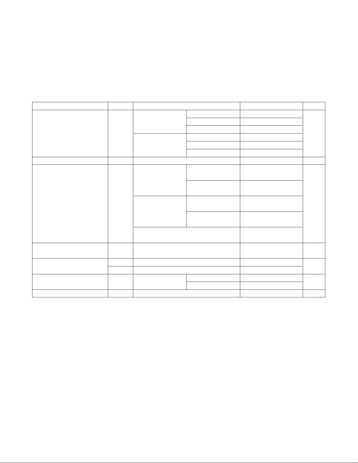
ELECTRICAL CHARACTERISTICS (continued)
(Typical Operating Circuit (Inverter), VDD= +5V, –S—H—D—N–= VDD, FC = LV = GND, C1 = C2 = 10µF (Note 2), TA= T
MIN
to T
MAX
, unless
otherwise noted. Typical values are at T
A
= +25°C.)
Note 2: C1 and C2 are low-ESR (<0.2Ω) aluminum electrolytics. Capacitor ESR adds to the circuit’s output resistance. Using
capacitors with higher ESR may reduce output voltage and efficiency.
Note 3: MAX860/MAX861 may draw high supply current during startup, up to the minimum operating supply voltage. To guaran-
tee proper startup, the input supply must be capable of delivering 90mA more than the maximum load current.
Note 4: Specified output resistance includes the effect of the 0.2Ω ESR of the test circuit’s capacitors.
Note 5: The switches are driven directly at the oscillator frequency, without any division.
Note 6: At lowest frequencies, using 10µF capacitors gives worse efficiency figures than using the recommended capacitor
values in Table 3, due to larger 1 ⁄ (f
s
x C1) term in R
OUT
.
–
S—H—D—N–< 0.3V
MAX860
LV = GND
No load
MAX860/MAX861, FC = VDD,
IL= 50mA to GND, C1 = C2 = 68µF
MAX860,
FC = V
DD
MAX861,
FC = V
DD
MAX861
FC < 4V
CONDITIONS
µA
10
Shutdown Supply Current
1
V
0.3V
IL
–
S—H—D—N–Threshold
1.2V
IH
%99 99.9Voltage-Conversion Efficiency
%
87
Power Efficiency (Note 6)
88 92
93 96
80 130
30 50
36
90 93
93 96
813
60 100
kHz
160 250
f
S
Switching Frequency
(Note 5)
µA-2 -4I
FC
FC Current (from VDD)
UNITSMIN TYP MAXSYMBOLPARAMETER
No load, V
OUT
= -4V µs500Time to Exit Shutdown
FC = V
DD
FC = GND
FC = OUT
FC = V
DD
FC = GND
FC = OUT
RL= 2kΩ from V
DD
to OUT
RL= 1kΩ from OUT
to GND
RL= 2kΩ from V
DD
to OUT
RL= 1kΩ from OUT
to GND
MAX86_I/E
MAX86_M
Page 4
MAX860/MAX861
50mA, Frequency-Selectable,
Switched-Capacitor Voltage Converters
4
Maxim Integrated
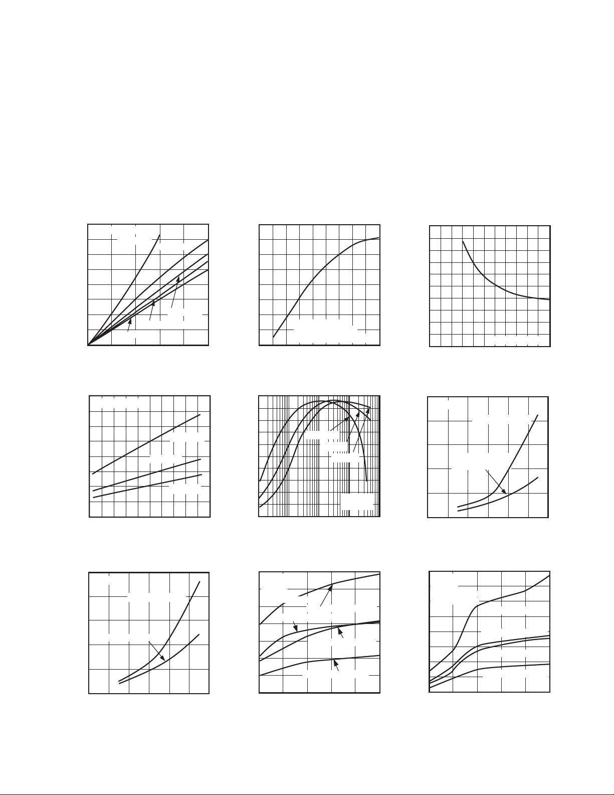
__________________________________________Typical Operating Characteristics
(All curves generated using the inverter circuit shown in the
Typical Operating Circuits
with LV = GND and TA= +25°C, unless other-
wise noted. Test results also valid for doubler mode with LV = OUT and T
A
= +25°C. All capacitor values used are those recom-
mended in Table 3, unless otherwise noted. The output resistance curves represent the resistance of the device itself, which is R
O
in
the equation for R
OUT
shown in the
Capacitor Selection
section.)
80
70
0
0.33
MAX860 OUTPUT CURRENT vs. CAPACITANC
MEDIUM-FREQUENCY MODE
MAX860-09
CAPACITANCE (μF)
OUTPUT CURRENT (mA)
4.7
40
20
1 2.2 22
60
10
10
30
50
VIN = +4.5V, V
OUT
= -3.5V
VIN = +3V, V
OUT
= -2.4V
VIN = +4.5V, V
OUT
= -4V
VIN = +3V, V
OUT
= -2.7V
f
OSC
= 50kHz
FC = GND
LV = GND
INVERTER MODE
OUTPUT VOLTAGE DROP FROM
SUPPLY VOLTAGE vs. LOAD CURRENT
0.8
0.7
0.6
0.5
0.4
DROP (V)
OUT
0.3
V
0.2
0.1
0
ALL FREQUENCIES
VDD = +1.5V
VDD = +4.5V, +5.0V
VDD = +5.5V
10 20 50
0
LOAD CURRENT (mA)
30
VDD = +2.5V
VDD = +3.5V
40
MAX860-01
= +5V)
DD
-2
-4
-6
-8
-10
-12
PERCENTAGE FREQUENCY CHANGE (%)
(FROM FREQUENCY MEASURED WITH V
-14
OUTPUT SOURCE RESISTANCE (RO) vs.
TEMPERATURE
MAX860-04
100
90
80
70
60
50
40
EFFICIENCY (%)
30
20
10
0
32
ALL FREQUENCIES
28
24
20
16
12
8
OUTPUT SOURCE RESISTANCE (Ω)
4
0
-60 -20 40 140
-40 0 60 80 120
VDD = +3V
20 100
TEMPERATURE (°C)
VDD = +1.5V
VDD = +5V
OSCILLATOR FREQUENCY vs.
SUPPLY VOLTAGE
2
0
ALL FREQUENCIES,
LV CONNECTED TO GND
(INVERTER) OR OUT (DOUBLER)
1.5 2.0 3.0 4.0
1.0
2.5 3.5
SUPPLY VOLTAGE (V)
4.5 5.0 5.5
MAX860
EFFICIENCY vs. LOAD CURRENT
VDD = +1.5V
VDD = +3V
VDD = +5V
INVERTER
FC = V
DD
0.01 1 100
0.1 10
LOAD CURRENT (mA)
OUTPUT SOURCE RESISTANCE (RO) vs.
SUPPLY VOLTAGE
20
MAX860-02
18
16
14
12
10
8
6
4
OUTPUT SOURCE RESISTANCE (Ω)
2
0
01 3 5
SUPPLY VOLTAGE (V)
ALL FREQUENCIES
24
MAX860 SUPPLY CURRENT
vs. SUPPLY VOLTAGE
500
FC = V
MAX860-05
400
300
200
SUPPLY CURRENT (μA)
100
DD
DOUBLER, LV = OUT
INVERTER, LV = GND
> 3V)
(V
DD
0
0
123 456
SUPPLY VOLTAGE (V)
MAX860-03
MAX860-06
MAX861 SUPPLY CURRENT
vs. SUPPLY VOLTAGE
500
FC = V
DD
400
300
SUPPLY CURRENT (μA)
200
100
0
0
INVERTER, LV = GND
123 456
SUPPLY VOLTAGE (V)
DOUBLER, LV = OUT
70
MAX860-07
60
50
40
30
OUTPUT CURRENT (mA)
20
10
MAX860 OUTPUT CURRENT vs. CAPACITANCE
HIGH-FREQUENCY MODE
f
= 130kHz
OSC
FC = OUT
LV = GND
INVERTER MODE
VIN = +4.5V, V
0
0.33
VIN = +4.5V, V
= -4V
OUT
VIN = +3V, V
VIN = +3V, V
1 2.2 22
CAPACITANCE (μF)
= -3.5V
OUT
= -2.4V
OUT
= -2.7V
OUT
4.7
10
MAX860-08
Page 5
MAX860/MAX861
50mA, Frequency-Selectable,
Switched-Capacitor Voltage Converters
5
Maxim Integrated
______________________________________________________________Pin Description
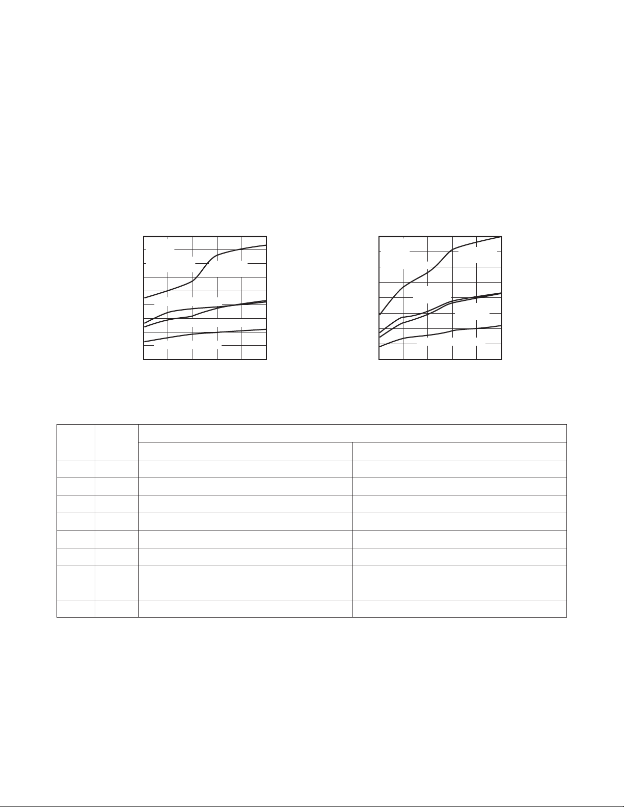
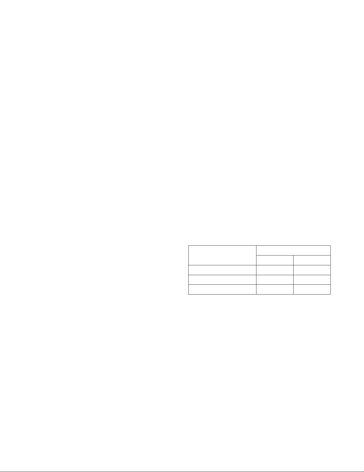
____________________________Typical Operating Characteristics (continued)
(All curves generated using the inverter circuit shown in the
Typical Operating Circuits
with LV = GND and TA= +25°C, unless other-
wise noted. Test results also valid for doubler mode with LV = OUT and T
A
= +25°C. All capacitor values used are those recom-
mended in Table 3, unless otherwise noted. The output resistance curves represent the resistance of the device itself, which is R
O
in
the equation for R
OUT
shown in the
Capacitor Selection
section.)
INVERTER
DOUBLER
Doubled Positive Output
Flying-Capacitor Negative Terminal
Ground
Low-Voltage-Operation Input. Connect to OUT.
Active-Low Shutdown Input. Connect to GND pin if not
used. Connect to OUT to disable the charge pump.
Positive Input Supply
Flying-Capacitor Positive Terminal
Frequency Control, see Table 1
FUNCTION
Positive Input SupplyV
DD
8
Flying-Capacitor Negative TerminalC1-4
Negative OutputOUT5
Low-Voltage-Operation Input. Connect to GND.LV6
Active-Low Shutdown Input. Connect to VDDif not
used. Connect to GND to disable the charge pump.
–
S—H—D—N
–
7
GroundGND3
Flying-Capacitor Positive Terminal C1+2
Frequency Control, see Table 1FC1
NAMEPIN
MAX861
OUTPUT CURRENT vs. CAPACITANCE
HIGH-FREQUENCY MODE
90
f
= 250kHz
OSC
80
FC = OUT
LV = GND
70
INVERTER MODE
60
50
40
30
OUTPUT CURRENT (mA)
20
10
VIN = +4.5V, V
VIN = +3V, V
0
0.33
1 2.2 22
CAPACITANCE (μF)
= -4V
OUT
VIN = +3V, V
= -2.7V
OUT
VIN = +4.5V,
= -3.5V
V
OUT
= -2.4V
OUT
4.7
10
MAX860-10
MAX861
OUTPUT CURRENT vs. CAPACITANCE
MEDIUM-FREQUENCY MODE
80
f
= 100kHz
OSC
FC = GND
70
LV = GND
INVERTER MODE
60
50
40
30
OUTPUT CURRENT (mA)
20
10
0
0.33
VIN = +3V,
= -2.4V
V
OUT
VIN = +3V, V
1 2.2 22
CAPACITANCE (μF)
VIN = +4.5V,
V
OUT
VIN = +4.5V,
V
OUT
= -2.7V
OUT
4.7
= -3.5V
MAX860-11
= -4V
10
Page 6
MAX860/MAX861
50mA, Frequency-Selectable,
Switched-Capacitor Voltage Converters
6
Maxim Integrated
_______________Detailed Description
The MAX860/MAX861 capacitive charge pumps either
invert or double the voltage applied to their inputs. For
highest performance, use low equivalent series resistance (ESR) capacitors. See the
Capacitor Selection
section for more details. The frequency-control (FC) pin
allows you to choose one of three switching frequencies; these three selectable frequencies are different for
each device. When shut down, MAX860/MAX861 current consumption reduces to less than 1µA.
Common Applications
Voltage Inverter
The most common application for these devices is a
charge-pump voltage inverter (see
Typical Operating
Circuits
). This application requires only two external components—capacitors C1 and C2—plus a bypass capacitor
if necessary (see
Bypass Capacitor
section). Refer to the
Capacitor Selection
section for suggested capacitor types
and values.
Even though the MAX860/MAX861’s output is not actively
regulated, it is fairly insensitive to load-current changes. A
circuit output source resistance of 12Ω (calculated using
the formula given in the
Capacitor Selection
section)
means that, with a +5V input, the output voltage is -5V
under no load and decreases to -4.4V with a 50mA load.
The MAX860/MAX861 output source resistance (used to
calculate the circuit output source resistance) vs. temperature and supply voltage are shown in the
Typical
Operating Characteristics
graphs.
Calculate the output ripple voltage using the formula
given in the
Capacitor Selection
section.
Positive Voltage Doubler
The MAX860/MAX861 can also operate as positive voltage doublers (see
Typical Operating Circuits
). This
application requires only two external components,
capacitors C1 and C2. The no-load output is twice the
input voltage. The electrical specifications in the doubler
mode are very similar to those of the inverter mode
except for the Supply Voltage Range (see
Electrical
Characteristics
table) and No-Load Supply Current (see
graph in
Typical Operating Characteristics
). The circuit
output source resistance and output ripple voltage are
calculated using the formulas in the
Capacitor Selection
section.
Active-Low Shutdown Input
When driven low, the –S—H—D—N–input shuts down the
device. In inverter mode, connect –S—H—D—N–to VDDif it is
not used. In doubler mode, connect –S—H—D—N–to GND if it
is not used. When the device is shut down, all active
circuitry is turned off.
In the inverting configuration, loads connected from
OUT to GND are not powered in shutdown mode.
However, a reverse-current path exists through two
diodes between OUT and GND; therefore, loads connected from V
DD
to OUT draw current from the input
supply.
In the doubling configuration, loads connected from the
VDDpin to the GND pin are not powered in shutdown
mode. Loads connected from the VDDpin to the OUT
pin draw current from the input supply through a path
similar to that of the inverting configuration (described
above).
Frequency Control
Charge-pump frequency for both devices can be set to
one of three values. Each device has a unique set of
three available frequencies, as indicated in Table 1.
The oscillator and charge-pump frequencies are the
same (i.e., the charge-pump frequency is not half the
oscillator frequency, as it is on the MAX660, MAX665,
and ICL7660).
*See the Electrical Characteristics for detailed switchingfrequency specifications.
A higher switching frequency minimizes capacitor size
for the same performance and increases the supply
current (Table 2). The lowest fundamental frequency of
the switching noise is equal to the minimum specified
switching frequency (e.g., 3kHz for the MAX860 with FC
open). The spectrum of noise frequencies extends
above this value because of harmonics in the switching
waveform. To get best noise performance, choose the
device and FC connection to select a minimum switching frequency that lies above your sensitive bandwidth.
Low-Voltage-Operation Input
LV should be connected to GND for inverting operation.
To enhance compatibility with the MAX660, MAX665, and
ICL7660, you may float LV if the input voltage exceeds 3V.
In doubling mode, LV must be connected to OUT for all
input voltages.
FREQUENCY (kHz)
FC CONNECTION
MAX860 MAX861
FC = VDDor open 6 13
FC = GND 50 100
FC = OUT 130 250
Table 1. Nominal Switching Frequencies*
Page 7
MAX860/MAX861
50mA, Frequency-Selectable,
Switched-Capacitor Voltage Converters
7
Maxim Integrated
__________Applications Information
Capacitor Selection
The MAX860/MAX861 are tested using 10µF capacitors
for both C1 and C2, although smaller or larger values
can be used (Table 3). Smaller C1 values increase the
output resistance; larger values reduce the output
resistance. Above a certain point, increasing the
capacitance of C1 has a negligible effect (because the
output resistance becomes dominated by the internal
switch resistance and the capacitor ESR). Low-ESR
capacitors provide the lowest output resistance and
ripple voltage. The output resistance of the entire circuit
(inverter or doubler) is approximately:
R
OUT
= RO+ 4 x ESRC1+ ESRC2+ 1 / (fSx C1)
where RO(the effective resistance of the MAX860/
MAX861’s internal switches) is approximately 8Ω and f
S
is the switching frequency. R
OUT
is typically 12Ω when
using capacitors with 0.2Ω ESR and fS, C1, and C2 values suggested in Table 3. When C1 and C2 are so
large (or the switching frequency is so high) that the
internal switch resistance dominates the output resistance, estimate the output resistance as follows:
R
OUT
= RO+ 4 x ESRC1+ ESR
C2
A typical design procedure is as follows:
1) Choose C1 and C2 to be the same, for convenience.
2) Select fS:
a) If you want to avoid a specific noise frequency,
choose f
S
appropriately.
b) If you want to minimize capacitor cost and size,
choose a high f
S
.
c) If you want to minimize current consumption,
choose a low fS.
3) Choose a capacitor based on Table 3, although
higher or lower values can be used to optimize performance. Table 4 lists manufacturers who provide
low-ESR capacitors.
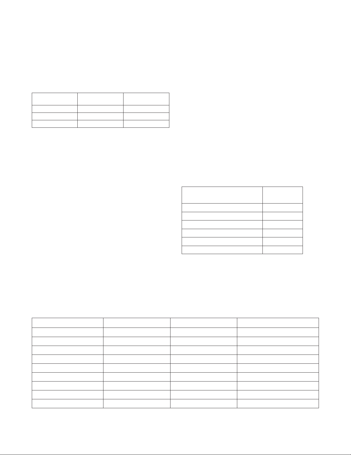
*In addition to Table 3, four graphs in the
Typical
Operating Characteristics
section show typical output
current for C1 and C2 capacitances ranging from
0.33µF to 22µF. Output current is plotted for inputs of
4.5V (5V - 10%) and 3.0V (3.3V - 10%), and also for
10% and 20% output droop from the ideal -VINvalue.
ATTRIBUTE
LOWER
FREQUENCY
HIGHER
FREQUENCY
Output Ripple Larger Smaller
C1, C2 Values Larger Smaller
Supply Current Smaller Larger
C1, C2 (μF)NOMINAL FREQUENCY (kHz)
6 68
13 47
50 10
100 4.7
130 4.7
250 2.2
Table 2. Switching-Frequency Trade-Offs
Table 3. Suggested Capacitor Values*
Table 4. Low-ESR Capacitor Manufacturers
MANUFACTURER–Series PHONE FAX COMMENTS
AVX TPS Series (803) 946-0629 (803) 626-3123 Low-ESR tantalum, SMT
AVX TAG Series (803) 946-0629 (803) 626-3123 Low-cost tantalum, SMT
Matsuo 267 Series (714) 969-2491 (714) 960-6492 Low-cost tantalum, SMT
Sprague 595 Series (603) 224-1961 (613) 224-1430 Low-ESR tantalum, SMT
Sanyo MV-GX Series (619) 661-6835 (619) 661-1055 Aluminum electrolytic, through hole
Sanyo CV-GX Series (619) 661-6835 (619) 661-1055 Aluminum electrolytic, SMT
Nichicon PL Series (847) 843-7500 (847) 843-2798 Aluminum electrolytic, through hole
United Chemicon (Marcon) (847) 696-2000 (847) 696-9278 Ceramic SMT
TDK (847) 390-4461 (847) 390-4405 Ceramic SMT
Page 8
MAX860/MAX861
50mA, Frequency-Selectable,
Switched-Capacitor Voltage Converters
8
Maxim Integrated
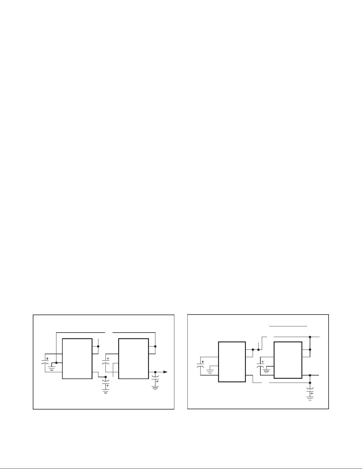
Figure 2. Paralleling MAX860s or MAX861s to Reduce Output
Resistance
Figure 1. Cascading MAX860s or MAX861s to Increase
Output Voltage
Flying Capacitor, C1
Increasing the size of the flying capacitor reduces the
output resistance.
Output Capacitor, C2
Increasing the size of the output capacitor reduces the
output ripple voltage. Decreasing its ESR reduces both
output resistance and ripple. Smaller capacitance values can be used if one of the higher switching frequencies is selected, if less than the maximum rated output
current (50mA) is required, or if higher ripple can be
tolerated. The following equation for peak-to-peak ripple applies to both the inverter and doubler circuits.
I
OUT
V
RIPPLE
= ———————— + 2 x I
OUT
x ESR
C2
2 x fSx C2
Bypass Capacitor
Bypass the incoming supply to reduce its AC impedance
and the impact of the MAX860/MAX861’s switching
noise. The recommended bypassing depends on the circuit configuration and where the load is connected.
When the inverter is loaded from OUT to GND or the
doubler is loaded from VDDto GND, current from the
supply switches between 2 x I
OUT
and zero. Therefore,
use a large bypass capacitor (e.g., equal to the value
of C1) if the supply has a high AC impedance.
When the inverter and doubler are loaded from VDDto
OUT, the circuit draws 2 x I
OUT
constantly, except for
short switching spikes. A 0.1µF bypass capacitor is
sufficient.
Cascading Devices
Two devices can be cascaded to produce an even
larger negative voltage, as shown in Figure 1. The
unloaded output voltage is nominally -2 x V
IN
, but this is
reduced slightly by the output resistance of the first
device multiplied by the quiescent current of the second. The output resistance of the complete circuit is
approximately
five times
the output resistance of a sin-
gle MAX860/MAX861.
Three or more devices can be cascaded in this way,
but output resistance rises dramatically, and a better
solution is offered by inductive switching regulators
(such as the MAX755, MAX759, MAX764, or MAX774).
Connect LV as with a standard inverter circuit (see
Pin
Description
).
The maximum load current and startup current of nth
cascaded circuit must not exceed the maximum output
current capability of (n-1)th circuit to ensure proper
startup.
Paralleling Devices
Paralleling multiple MAX860s or MAX861s reduces the
output resistance. As illustrated in Figure 2, each
device requires its own pump capacitor (C1), but the
reservoir capacitor (C2) serves all devices. C2’s value
should be increased by a factor of n, where n is the
number of devices. Figure 2 shows the equation for calculating output resistance. An alternative solution is to
use the MAX660 or MAX665, which are capable of supplying up to 100mA of load current. Connect LV as with
a standard inverter circuit (see
Pin Description
).
Combined Doubler/Inverter
In the circuit of Figure 3, capacitors C1 and C2 form the
inverter, while C3 and C4 form the doubler. C1 and C3
are the pump capacitors; C2 and C4 are the reservoir
capacitors. Because both the inverter and doubler use
part of the charge-pump circuit, loading either output
causes both outputs to decline towards GND. Make
…
+V
IN
8
22
MAX860
MAX861
C1
33
“1”
445
7
C1
MAX860
MAX861
“n”
8
7
5
…
C2
= -nV
V
OUT
IN
OF SINGLE DEVICE
R
OUT
R
=
OUT
NUMBER OF DEVICES
…
+V
IN
8
22
MAX860
MAX861
33
V
OUT
C2
“1”
445
7
C1C1
MAX860
MAX861
“n”
…
V
OUT
8
7
5
= -V
IN
V
OUT
C2
Page 9
MAX860/MAX861
50mA, Frequency-Selectable,
Switched-Capacitor Voltage Converters
Table 5. Product Selection Guide
+V
IN
8
2
MAX860
MAX861
C1
3
4
7
5
D1, D2 = 1N4148
D1
V
= -V
OUT
IN
C2
PART
NUMBER
MAX660 100 6.5 5/40
MAX665 100 6.5 5/40
OUTPUT
CURRENT
(mA)
OUTPUT
RESISTANCE
(Ω)
SWITCHING
FREQUENCY
(kHz)
D2
C3
Figure 3. Combined Doubler and Inverter
V
= (2VIN) -
OUT
(V
) - (V
FD2
)
FD1
C4
sure the sum of the currents drawn from the two outputs does not exceed 60mA. Connect LV as with a
standard inverter circuit (see
Pin Description
).
Compatibility with
MAX660/MAX665/ICL7660
The MAX860/MAX861 can be used in sockets
designed for the MAX660, MAX665, and ICL7660 with
a minimum of one wiring change. This section gives
advice on installing a MAX860/MAX861 into a socket
designed for one of the earlier devices.
The MAX660, MAX665, and ICL7660 have an OSC pin
instead of –S—H—D—N–. MAX660, MAX665, and ICL7660 normal operation is with OSC floating (although OSC can
be overdriven). If OSC is floating, pin 7 (–S—H—D—N–) should
be jumpered to VDDto enable the MAX860/MAX861
permanently. Do not leave –S—H—D—N–on the MAX860/
MAX861 floating.
The MAX860/MAX861 operate with FC either floating or
connected to VDD, OUT, or GND; each connection
defines the oscillator frequency. Thus, any of the normal MAX660, MAX665, or ICL7660 connections to pin 1
will work with the MAX860/MAX861, without modifications. Changes to the FC connection are only required
if you want to adjust the operating frequency.
MAX860 50 12 6/50/130
MAX861 50 12 13/100/250
ICL7660 10 55 5
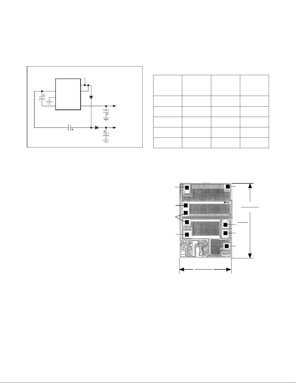
___________________Chip Topography
FC
C1+
GND
C1-
0.058"
(1.47mm)
PROCESS: BiCMOS
SUBSTRATE CONNECTED TO V
DD
V
DD
0.084"
(2.13mm)
SHDN
LV
OUT
Maxim Integrated
9
Page 10
MAX860/MAX861
50mA, Frequency-Selectable,
Switched-Capacitor Voltage Converters
10
Maxim Integrated
Package Information
For the latest package outline information and land patterns (footprints), go to www.maximintegrated.com/packages. Note that a “+”, “#”, or
“-” in the package code indicates RoHS status only. Package drawings may show a different suffix character, but the drawing pertains to the
package regardless of RoHS status.
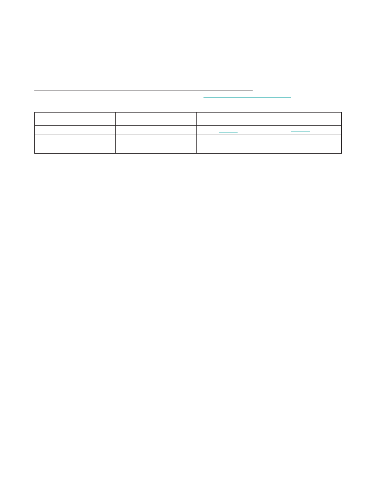
PACKAGE TYPE PACKAGE CODE OUTLINE NO.
LAND
PATTERN NO.
8 SO S8-4
21-0041
90-0096
8 CDIP J8-2
21-0045 —
8 µMAX U8-1
21-0036 90-0092
Page 11
Maxim Integrated cannot assume responsibility for use of any circuitry other than circuitry entirely embodied in a Maxim Integrated product. No circuit patent
licenses are implied. Maxim Integrated reserves the right to change the circuitry and specifications without notice at any time. The parametric values (min and
max limits) shown in the Electrical Characteristics table are guaranteed. Other parametric values quoted in this data sheet are provided for guidance.
Maxim Integrated 160 Rio Robles, San Jose, CA 95134 USA 1-408-601-1000 ________________________________
11
© 2013 Maxim Integrated Products, Inc. Maxim Integrated and the Maxim Integrated logo are trademarks of Maxim Integrated Products, Inc.
MAX860/MAX861
50mA, Frequency-Selectable,
Switched-Capacitor Voltage Converters
Revision History
REVISION
NUMBER
0 7/94 Initial release —
2 4/03 Updated Electrical Characteristics and Cascading Devices section. 3, 8
3 8/13
REVISION
DATE
DESCRIPTION
Added MAX860MSA/PR3 to data sheet and revised Absolute Maximum
Ratings.
PAGES
CHANGED
1, 2
 Loading...