

Page 1
General Description
The MAX8588 power-management IC is optimized for
devices using Intel X-Scale™ microprocessors, including smartphones, PDAs, internet appliances, and other
portable devices requiring substantial computing and
multimedia capability at low power.
The IC integrates seven high-performance, low-operatingcurrent power supplies along with supervisory and
management functions. Included are three step-down
DC-DC outputs, three linear regulators, and a seventh
always-on output. DC-DC converters power I/O, memory, and the CPU core. The I/O supply can be preset to
3.3V or adjusted to other values. The DRAM supply is
preset for 3.3V or 2.5V, or it can be adjusted with external resistors. The CPU core supply is serial programmed for dynamic voltage management and can
supply up to 0.5A. Linear-regulated outputs are provided for SRAM, PLL, and USIM supplies.
To minimize quiescent current, critical power supplies
have bypass “sleep” LDOs that can be activated when
output current is very low. Other functions include separate on/off control for all DC-DC converters, low-battery and dead-battery detection, a reset and power-OK
output, a backup-battery input, and a two-wire serial
interface.
All DC-DC outputs use fast, 1MHz PWM switching and
small external components. They operate with fixed-frequency PWM control and automatically switch from
PWM to skip-mode operation at light loads to reduce
operating current and extend battery life. The core output can be forced into PWM mode at all loads to minimize noise. A 2.6V to 5.5V input voltage range allows
1-cell lithium-ion (Li+), 3-cell NiMH, or a regulated 5V
input. The MAX8588 is available in a tiny 6mm x 6mm,
48-pin thin QFN package.
Applications
PDA, Palmtop, and Wireless Handhelds
Third-Generation Smart Cell Phones
Internet Appliances and Web-Books
Features
♦ Six Regulators in One Package
Step-Down DC-DC for I/O at 1.3A
Step-Down DC-DC for Memory at 0.9A
Step-Down Serial-Programmed DC-DC for CORE
Up to 0.5A
Three LDO Outputs for SRAM, PLL, and USIM
Always-On Output for VCC_BATT
♦ Low Operating Current
60µA in Sleep Mode (Sleep LDOs On)
130µA with DC-DCs On (Core Off)
200µA All Regulators On, No Load
5µA Shutdown Current
♦ Optimized for X-Scale Processors
♦ Backup-Battery Input
♦ 1MHz PWM Switching Allows Small External
Components
♦ Tiny 6mm x 6mm, 48-Pin Thin QFN Package
MAX8588
High-Efficiency, Low-I
Q
PMIC with
Dynamic Core for PDAs and Smartphones
________________________________________________________________ Maxim Integrated Products 1
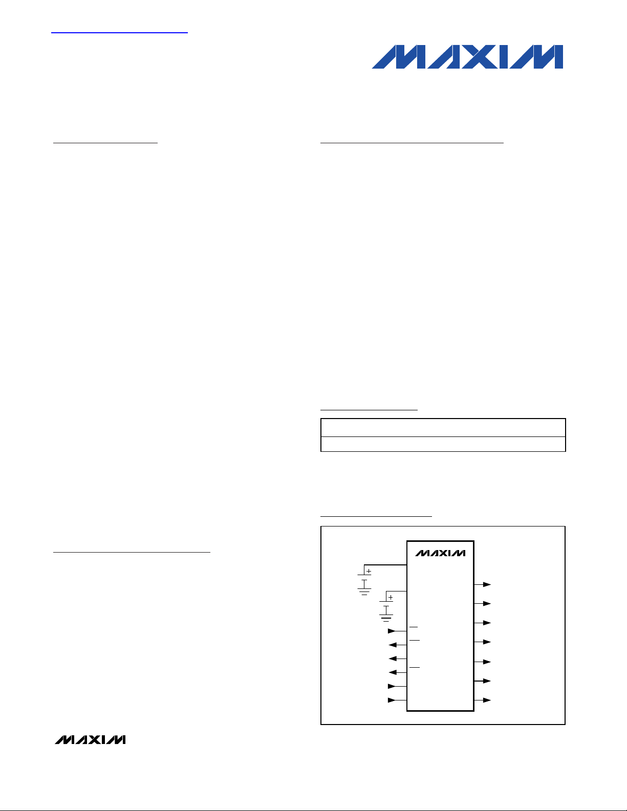
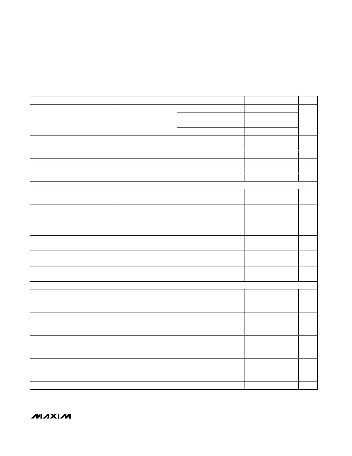
Simplified Diagram
19-3527; Rev 0; 3/05
For pricing, delivery, and ordering information, please contact Maxim/Dallas Direct! at
1-888-629-4642, or visit Maxim’s website at www.maxim-ic.com.
Pin Configuration appears at end of data sheet.
X-Scale is a trademark of Intel Corp.
Ordering Information
查询MAX8588ETM供应商
PART TEMP RANGE PIN-PACKAGE
MAX8588ETM -40°C to +85°C 48 Thin QFN (6mm x 6mm)
MAIN BATTERY
nRESET
nVCC_FAULT
nBATT_FAULT
SYS_EN
PWR_EN
BACKUP
BATTERY
IN
BKBT
MR
RSO
POK
DBO
ON1-2
ON3-6
MAX8588
V1
V2
V3
V4
V5
V6
V7
VCC_IO 3.3V
VCC_MEM 2.5V
VCC_CORE
0.8V TO 1.3V
VCC_PLL 1.3V
VCC_SRAM 1.1V
VCC_USIM
0V, 1.8V, 3.0V
VCC_BATT
Page 2
MAX8588
High-Efficiency, Low-IQPMIC with
Dynamic Core for PDAs and Smartphones
2 _______________________________________________________________________________________
ABSOLUTE MAXIMUM RATINGS
ELECTRICAL CHARACTERISTICS
(VIN= 3.6V, V
BKBT
= 3.0V, V
LBI
= 1.1V, V
DBI
= 1.35V, circuit of Figure 5, TA = 0°C to +85°C, unless otherwise noted. Typical values
are at T
A
= +25°C.)
Stresses beyond those listed under “Absolute Maximum Ratings” may cause permanent damage to the device. These are stress ratings only, and functional
operation of the device at these or any other conditions beyond those indicated in the operational sections of the specifications is not implied. Exposure to
absolute maximum rating conditions for extended periods may affect device reliability.
IN, IN45, IN6, MR, LBO, DBO, RSO, POK, SCL, SDA,
BKBT, V7, SLP, SRAD, PWM3 to GND...............-0.3V to +6V
REF, CC_, ON_, FB_, DBI, LBI, V1, V2, RAMP, BYP,
MR to GND ...........................................-0.3V to (V
IN
+ 0.3V)
PV1, PV2, PV3, SLPIN to IN...................................-0.3V to +0.3V
V4, V5 to GND ..........................................-0.3V to (V
IN45
+ 0.3V)
V6 to GND ..................................................-0.3V to (V
IN6
+ 0.3V)
PV1 to PG1 ............................................................-0.3V to +6.0V
PV2 to PG2 ............................................................-0.3V to +6.0V
PV3 to PG3 ............................................................-0.3V to +6.0V
LX1 Continuous Current....................................-1.30A to +1.30A
LX2 Continuous Current........................................-0.9A to +0.9A
LX3 Continuous Current........................................-0.5A to +0.5A
PG1, PG2, PG3 to GND.........................................-0.3V to +0.3V
V1, V2, V4, V5, V6 Output Short-Circuit Duration.......Continuous
Continuous Power Dissipation (T
A
= +70°C)
6mm x 6mm 48-Pin Thin QFN
(derate 26.3mW/°C above +70°C)...........................2105mW
Operating Temperature Range ...........................-40°C to +85°C
Junction Temperature......................................................+150°C
Storage Temperature Range .............................-65°C to +150°C
Lead Temperature (soldering, 10s) .................................+300°C
PV1, PV2, PV3, SLPIN, IN Supply
Voltage Range
IN45, IN6 Supply Voltage Range 2.4 5.5 V
IN Undervoltage-Lockout (UVLO)
Threshold
Quiescent Current
BKBT Input Current
REF Output Voltage 0 to 10µA load 1.2375 1.25 1.2625 V
SYNCHRONOUS-BUCK PWM REG1
REG1 Voltage Accuracy FB1 = GND, 3.6V ≤ V
FB1 Voltage Accuracy
FB1 Input Current FB1 used with external resistors 100 nA
Error-Amplifier Transconductance Referred to FB 87 µS
Dropout Voltage (Note 1)
PARAMETER CONDITIONS MIN TYP MAX UNITS
PV1, PV2, PV3, IN, and SLPIN must connect together
externally
V
rising 2.25 2.40 2.55
IN
falling 2.200 2.35 2.525
V
IN
+ I
PV3
PV1
+ I
IN45
+
+
IN
+
PV1
No load (I
I
+ I
PV2
I
SLPIN
I
)
IN6
ON1 = 0 4
ON1 = IN 0.8
FB1 used with external resistors, 3.6V ≤ V
load = 0 to 1300mA
Load = 800mA 180 280
Load = 1300mA 293 450
Only V7 on, V
REG1 and REG2 on in switch mode,
REG3 off
REG1 and REG2 on in sleep mode,
REG3 off
All REGs on 225
≤ 5.5V, load = 0 to 1300mA 3.25 3.3 3.35 V
= 3.0V 32
IN
≤ 5.5V,
PV1
2.6 5.5 V
130
60
1.231 1.25 1.269 V
V
µA
µA
mV
Page 3
MAX8588
High-Efficiency, Low-I
Q
PMIC with
Dynamic Core for PDAs and Smartphones
_______________________________________________________________________________________ 3
ELECTRICAL CHARACTERISTICS (continued)
(VIN= 3.6V, V
BKBT
= 3.0V, V
LBI
= 1.1V, V
DBI
= 1.35V, circuit of Figure 5, TA = 0°C to +85°C, unless otherwise noted. Typical values
are at T
A
= +25°C.)
p-Channel On-Resistance
n-Channel On-Resistance
Current-Sense Transresistance 0.5 V/A
p-Channel Current-Limit Threshold -1.55 -1.80 -2.10 A
PWM Skip-Mode Transition Load
Current
OUT1 Maximum Output Current 2.6V ≤ V
LX1 Leakage Current V
SYNCHRONOUS-BUCK PWM REG2
REG2 Voltage Accuracy
FB2 Voltage Accuracy
FB2 Input Current FB2 used with external resistors, V
Error-Amplifier Transconductance Referred to FB 87 µS
Dropout Voltage Load = 900mA (Note 1) 243 380 mV
p-Channel On-Resistance
n-Channel On-Resistance
Current-Sense Transresistance 0.7 V/A
p-Channel Current-Limit Threshold -1.10 -1.275 -1.50 A
PWM Skip-Mode Transition Load
Current
OUT2 Maximum Output Current 2.6V ≤ V
LX2 Leakage Current V
SYNCHRONOUS-BUCK PWM REG3
REG3 Voltage Accuracy
Error-Amplifier Transconductance 68 µS
PARAMETER CONDITIONS MIN TYP MAX UNITS
I
= -180mA 0.18 0.3
LX1
I
= -180mA, V
LX1
I
= 180mA 0.13 0.225
LX1
I
= 180mA, V
LX1
Decreasing load current (Note 2) 30 mA
≤ 5.5V (Note 3) 1.3 A
PV1
= 5.5V, LX1 = GND or PV1, V
PV1
FB2 = GND, 3.6V ≤ V
FB2 = IN, 3.6V ≤ V
FB2 used with external resistors, 3.6V ≤ V
load = 0 to 900mA
I
= -180mA 0.225 0.375
LX2
= -180mA, V
I
LX2
I
= 180mA 0.15 0.25
LX2
= 180mA, V
I
LX2
Decreasing load current (Note 2) 30 mA
≤ 5.5V (Note 3) 0.9 A
PV2
= 5.5V, LX2 = GND or PV2, V
PV2
REG3 from 0.7V to 1.475V,
2.6V ≤ V
PV3
≤ 5.5V
= 2.6V 0.21 0.35
PV1
= 2.6V 0.15 0.25
PV1
= 0V -20 +0.1 +20 µA
ON1
≤ 5.5V, load = 0 to 900mA 2.463 2.5 2.537
PV2
≤ 5.5V, load = 0 to 900mA 3.25 3.3 3.35
PV2
≤ 5.5V,
PV2
= 1.25V 100 nA
FB2
= 2.6V 0.26 0.425
PV2
= 2.6V 0.17 0.275
PV2
= 0V -10 +0.1 +10 µA
ON2
Load = 0 to 500mA -1.5 +1.5 %
1.231 1.25 1.269 V
Ω
Ω
V
Ω
Ω
Page 4
MAX8588
High-Efficiency, Low-IQPMIC with
Dynamic Core for PDAs and Smartphones
4 _______________________________________________________________________________________
ELECTRICAL CHARACTERISTICS (continued)
(VIN= 3.6V, V
BKBT
= 3.0V, V
LBI
= 1.1V, V
DBI
= 1.35V, circuit of Figure 5, TA = 0°C to +85°C, unless otherwise noted. Typical values
are at T
A
= +25°C.)
p-Channel On-Resistance
n-Channel On-Resistance
Current-Sense Transresistance 1.1 V/A
p-Channel Current-Limit Threshold -0.60 -0.7 -0.85 A
PWM Skip-Mode Transition Load
Current
OUT3 Maximum Output Current 2.6V ≤ V
LX3 Leakage Current V
LDOS V4, V5, V6, V1 SLEEP, V2 SLEEP, AND V7 OUTPUT
V4, V5, V6, V1 SLEEP, V2 SLEEP
Output Current
V7 Output Current 30 mA
REG4 Output Voltage Load = 0.1mA to 35mA 1.261 1.3 1.339 V
REG4 Noise With 1µF C
REG5 Output Voltage Load = 0.1mA to 35mA 1.067 1.1 1.133 V
IN45, IN6 Input Voltage Range 2.4 5.5 V
REG6 Output Voltage (POR Default
to 0V, Set by Serial Input)
V7 Output Voltage
V1 and V2 SLEEP Output Voltage
Accuracy
V1 and V2 SLEEP Dropout Voltage Load = 20mA 75 150 mV
V6 Dropout Voltage 3V m od e, l oad = 30m A, 2.5V m od e, l oad = 30m A 110 200 mV
V7 Switch Voltage Drop Load = 20mA, V
V4, V5, V6 Output Current Limit 40 90 mA
BKBT Leakage 1 µA
OSCILLATOR
PWM Switching Frequency 0.93 1 1.07 MHz
SUPERVISORY/MANAGEMENT FUNCTIONS
POK Trip Threshold (Note 4)
PARAMETER CONDITIONS MIN TYP MAX UNITS
I
= -180mA 0.225 0.375
LX3
I
= -180mA, V
LX2
I
= 180mA 0.15 0.25
LX3
= 180mA, V
I
LX3
Decreasing load current (Note 2) 30 mA
≤ 5.5V (Note 3) 0.5 A
PV3
= 5.5V, LX3 = GND or PV2, V
PV3
OUT
0V setti ng ( ei ther ON 6 l ow or ser i al p r og r am m ed ) 0
1.8V setting, load = 0.1mA to 35mA 1.746 1.8 1.854
2.5V setting, load = 0.1mA to 35mA 2.425 2.5 2.575
3.0V setting, load = 0.1mA to 35mA 2.91 3.0 3.09
V1 on and in regulation V
V1 off V
Set to same output voltage as REG1 and REG2 -3.0 +3.0 %
Rising 92 94.75 97
Falling 88.5 90.5 92.5
= 2.6V 0.26 0.425
PV3
= 2.6V 0.17 0.275
PV3
= 0V -10 +0.1 +10 µA
ON3
35 mA
and 0.01µF C
= V
BKBT
V1
BYP
= 3.0V 100 200 mV
15 µV
BKBT
V1
Ω
Ω
RMS
V
V
%
Page 5
MAX8588
High-Efficiency, Low-I
Q
PMIC with
Dynamic Core for PDAs and Smartphones
_______________________________________________________________________________________ 5
ELECTRICAL CHARACTERISTICS (continued)
(VIN= 3.6V, V
BKBT
= 3.0V, V
LBI
= 1.1V, V
DBI
= 1.35V, circuit of Figure 5, TA = 0°C to +85°C, unless otherwise noted. Typical values
are at T
A
= +25°C.)
LBI Threshold (Falling) Hysteresis is 5% (typ)
DBI Threshold (Falling) Hysteresis is 5% (typ)
RSO Threshold (Falling) Voltage on REG7, hysteresis is 5% (typ) 2.25 2.41 2.56 V
RSO Deassert Delay 61 65.5 70 ms
LBI Input Bias Current -50 -5 nA
DBI Input Bias Current 15 50 nA
Thermal-Shutdown Temperature TJ rising +160 °C
Thermal-Shutdown Hysteresis 15 °C
LOGIC INPUTS AND OUTPUTS
LBO, DBO, POK, RSO, SDA Output
Low Level
LBO, DBO, POK, RSO Output Low
Level
LBO, DBO, POK, RSO Output-High
Leakage Current
ON_, SCL, SDA, SLP, PWM3, MR,
SRAD Input High Level
ON_, SCL, SDA, SLP, PWM3, MR,
SRAD Input Low Level
ON_, SCL, SDA, SLP, PWM3, MR,
SRAD Input Leakage Current
SERIAL INTERFACE
Clock Frequency 400 kHz
Bus Free Time Between START and
STOP
H ol d Ti m e Rep eated S TART C ond i ti on 0.6 µs
CLK Low Period 1.3 µs
CLK High Period 0.6 µs
S etup Ti m e Rep eated S TART C ond i ti on 0.6 µs
DATA Hold Time 0µs
DATA Setup Time 100 ns
Maximum Pulse Width of Spikes that
Must be Suppressed by the Input
Filter of Both DATA and CLK Signals
Setup Time for STOP Condition 0.6 µs
PARAMETER CONDITIONS MIN TYP MAX UNITS
LBI = IN (for preset) 3.51 3.6 3.69
With resistors at LBI 0.98 1.00 1.02
DBI = IN (for preset) 3.024 3.15 3.276
With resistors at LBI 1.208 1.232 1.256
2.6V ≤ V7
V7
Pin
2.6V ≤ V
2.6V ≤ V
Pin = GND, 5.5V -1 +1 µA
≤ 5.5V, sinking 1mA 0.4 V
= 1V, sinking 100µA 0.4 V
= 5.5V 0.2 µA
≤ 5.5V 1.6 V
IN
≤ 5.5V 0.4 V
IN
1.3 µs
50 ns
V
V
Page 6
MAX8588
High-Efficiency, Low-IQPMIC with
Dynamic Core for PDAs and Smartphones
6 _______________________________________________________________________________________
ELECTRICAL CHARACTERISTICS
(VIN= 3.6V, V
BKBT
= 3.0V, V
LBI
= 1.1V, V
DBI
= 1.35V, circuit of Figure 5, TA = -40°C to +85°C, unless otherwise noted.) (Note 5)
PV1, PV2, PV3, SLPIN, IN Supply
Voltage Range
IN45, IN6 Supply Voltage Range 2.4 5.5 V
IN Undervoltage-Lockout (UVLO)
Threshold
SYNCHRONOUS-BUCK PWM REG1
REG1 Voltage Accuracy FB1 = GND, 3.6V ≤ V
FB1 Voltage Accuracy
FB1 Input Current FB1 used with external resistors 100 nA
Dropout Voltage
p-Channel On-Resistance
n-Channel On-Resistance
p-Channel Current-Limit Threshold -1.55 -2.10 A
OUT1 Maximum Output Current 2.6V ≤ V
LX1 Leakage Current V
SYNCHRONOUS-BUCK PWM REG2
REG2 Voltage Accuracy
FB2 Voltage Accuracy
FB2 Input Current FB2 used with external resistors, V
Dropout Voltage Load = 900mA (Note 1) 380 mV
p-Channel On-Resistance
n-Channel On-Resistance
p-Channel Current-Limit Threshold -1.1 -1.50 A
OUT2 Maximum Output Current 2.6V ≤ V
LX2 Leakage Current V
PARAMETER CONDITIONS MIN MAX UNITS
PV1, PV2, PV3, IN, and SLPIN must connect together
externally
V
rising 2.25 2.55
IN
V
falling 2.200 2.525
IN
≤ 5.5V, load = 0 to 1300mA 3.25 3.35 V
PV1
FB1 used with external resistors, 3.6V ≤ V
load = 0 to 1300mA
Load = 800mA (Note 1) 280
Load = 1300mA (Note 1) 450
I
= -180mA 0.3
LX1
I
= -180mA, V
LX1
I
= 180mA 0.225
LX1
I
= 180mA, V
LX1
≤ 5.5V (Note 3) 1.30 A
PV1
= 5.5V, LX1 = GND or PV1, V
PV1
FB2 = GND, 3.6V ≤ V
FB2 = IN, 3.6V ≤ V
FB2 used with external resistors, 3.6V ≤ V
load = 0 to 900mA
I
= -180mA 0.375
LX2
= -180mA, V
I
LX2
I
= -180mA 0.25
LX2
= -180mA, V
I
LX2
≤ 5.5V (Note 3) 0.9 A
PV2
= 5.5V, LX2 = GND or PV2, V
PV2
= 2.6V 0.35
PV1
= 2.6V 0.25
PV1
ON1
≤ 5.5V, load = 0 to 900mA 2.463 2.537
PV2
≤ 5.5V, load = 0 to 900mA 3.25 3.35
PV2
FB2
= 2.6V 0.425
PV2
= 2.6V 0.275
PV2
ON2
≤ 5.5V,
PV1
= 0V -10 +10 µA
≤ 5.5V,
PV2
= 1.25V 100 nA
= 0V -10 +10 µA
2.6 5.5 V
1.231 1.269 V
1.231 1.269 V
V
mV
Ω
Ω
V
Ω
Ω
Page 7
MAX8588
High-Efficiency, Low-I
Q
PMIC with
Dynamic Core for PDAs and Smartphones
_______________________________________________________________________________________ 7
ELECTRICAL CHARACTERISTICS (continued)
(VIN= 3.6V, V
BKBT
= 3.0V, V
LBI
= 1.1V, V
DBI
= 1.35V, circuit of Figure 5, TA = -40°C to +85°C, unless otherwise noted.) (Note 5)
SYNCHRONOUS-BUCK PWM REG3
REG3 Output Voltage Accuracy
p-Channel On-Resistance
n-Channel On-Resistance
p-Channel Current-Limit Threshold -0.60 -0.85 A
OUT3 Maximum Output Current 2.6V ≤ V
LX3 Leakage Current V
LDOs V4, V5, V6, V1 SLEEP, V2 SLEEP, AND V7 OUTPUT
V4, V5, V6, V1 SLEEP, V2 SLEEP
Output Current
V7 Output Current 30 mA
REG4 Voltage Accuracy Load = 0.1mA to 35mA 1.254 1.346 V
REG5 Voltage Accuracy Load = 0.1mA to 35mA 1.061 1.139 V
IN45, IN6 Input Voltage Range 2.4 5.5 V
REG6 Output Voltage (POR Default
to 0V, Set by Serial Input)
V1 and V2 SLEEP Output Voltage
Accuracy
V1 and V2 SLEEP Dropout Voltage Load = 20mA 150 mV
V6 Dropout Voltage 3V m od e, l oad = 30m A; 2.5V m od e, l oad = 30m A 200 mV
V7 Switch Voltage Drop Load = 20mA, V
V4, V5, V6 Output Current Limit 40 mA
BKBT Leakage 1 µA
OSCILLATOR
PWM Switching Frequency 0.93 1.07 MHz
SUPERVISORY/MANAGEMENT FUNCTIONS
POK Trip Threshold (Note 4)
LBI Threshold (Falling) Hysteresis is 5% (typ)
PARAMETER CONDITIONS MIN MAX UNITS
REG3 from 0.7V to 1.475V,
2.6V ≤ V
I
LX3
I
LX2
I
LX3
I
LX3
PV3
1.8V setting, load = 0.1mA to 35mA 1.737 1.863
2.5V setting, load = 0.1mA to 35mA 2.412 2.588
3.0V setting, load = 0.1mA to 35mA 2.895 3.105
Set to same output voltage as REG1 and REG2 -3.5 +3.5 %
Rising 92 97
Falling 88.5 92.5
≤ 5.5V
PV3
= -180mA 0.375
= -180mA, V
= 180mA 0.25
= 180mA, V
≤ 5.5V (Note 3) 0.5 A
PV3
= 5.5V, LX3 = GND or PV2, V
= 2.6V 0.425
PV3
= 2.6V 0.275
PV3
BKBT
Load = 0 to 500mA -1.5 +1.5 %
= 0V -10 +10 µA
ON3
35 mA
= V
= 3.0V 200 mV
V1
LBI = IN (for preset) 3.51 3.69
With resistors at LBI 0.98 1.02
Ω
Ω
V
%
V
Page 8
MAX8588
High-Efficiency, Low-IQPMIC with
Dynamic Core for PDAs and Smartphones
8 _______________________________________________________________________________________
ELECTRICAL CHARACTERISTICS (continued)
(VIN= 3.6V, V
BKBT
= 3.0V, V
LBI
= 1.1V, V
DBI
= 1.35V, circuit of Figure 5, TA = -40°C to +85°C, unless otherwise noted.) (Note 5)
DBI Threshold (Falling) Hysteresis is 5% (typ)
RSO Threshold (Falling) Voltage on REG7, hysteresis is 5% (typ) 2.25 2.60 V
RSO Deassert Delay 62 69 ms
LBI Input Bias Current -50 nA
DBI Input Bias Current 75 nA
LOGIC INPUTS AND OUTPUTS
LBO, DBO, POK, RSO, SDA Output
Low Level
LBO, DBO, POK, RSO, SDA Output
Low Level
LBO, DBO, POK, RSO Output-High
Leakage Current
ON_, SCL, SDA, SLP, PWM3, MR,
SRAD Input High Level
ON_, SCL, SDA, SLP, PWM3, MR,
SRAD Input Low Level
ON_, SCL, SDA, SLP, PWM3, MR,
SRAD Input Leakage Current
SERIAL INTERFACE
Clock Frequency 400 kHz
Bus Free Time Between START and
STOP
Hold Time Repeated START
Condition
CLK Low Period 1.3 µs
CLK High Period 0.6 µs
Setup Time Repeated START
Condition
DATA Hold Time 0µs
DATA Setup Time 100 ns
Setup Time for STOP Condition 0.6 µs
PARAMETER CONDITIONS MIN MAX UNITS
DBI = IN (for preset) 2.993 3.307
With resistors at LBI 1.208 1.256
2.6V ≤ V7
V7
Pin
2.6V ≤ V
2.6V ≤ V
Pin = GND, 5.5V -1 +1 µA
≤ 5.5V, sinking 1mA 0.4 V
= 1V, sinking 100µA 0.4 V
= 5.5V 0.2 µA
≤ 5.5V 1.6 V
IN
≤ 5.5V 0.4 V
IN
1.3 µs
0.6 µs
0.6 µs
V
Page 9

MAX8588
High-Efficiency, Low-I
Q
PMIC with
Dynamic Core for PDAs and Smartphones
_______________________________________________________________________________________ 9
Note 1: Dropout voltage is guaranteed by the p-channel switch resistance and assumes a maximum inductor resistance of 45mΩ.
Note 2: The PWM-skip-mode transition has approximately 10mA of hysteresis.
Note 3: The maximum output current is guaranteed by the following equation:
where:
and R
N
= n-channel synchronous rectifier R
DS(ON)
RP = p-channel power switch R
DS(ON)
RL = external inductor ESR
I
OUT(MAX)
= maximum required load current
f = operating frequency minimum
L = external inductor value
I
LIM
can be substituted for I
OUT(MAX)
(desired) when solving for D. This assumes that the inductor ripple current is
small relative to the absolute value.
Note 4: POK only indicates the status of supplies that are enabled (except V7). When a supply is turned off, POK does not trigger
low. When a supply is turned on, POK immediately goes low until that supply reaches regulation. POK is forced low when all
supplies (except V7) are disabled.
Note 5: Specifications to -40°C are guaranteed by design, not production tested.
ELECTRICAL CHARACTERISTICS (continued)
VD
()
−
1
I
LIM
I
OUT
=
max
++
1
VI RR
++
OUT OUT MAX N L
D
=
VI RR
+−
IN OUT MAX N P
OUT
−
xfxL
2
()
−
RR
()
NL
()
()
1
xfxL
2
()
()
D
Page 10
MAX8588
High-Efficiency, Low-IQPMIC with
Dynamic Core for PDAs and Smartphones
10 ______________________________________________________________________________________
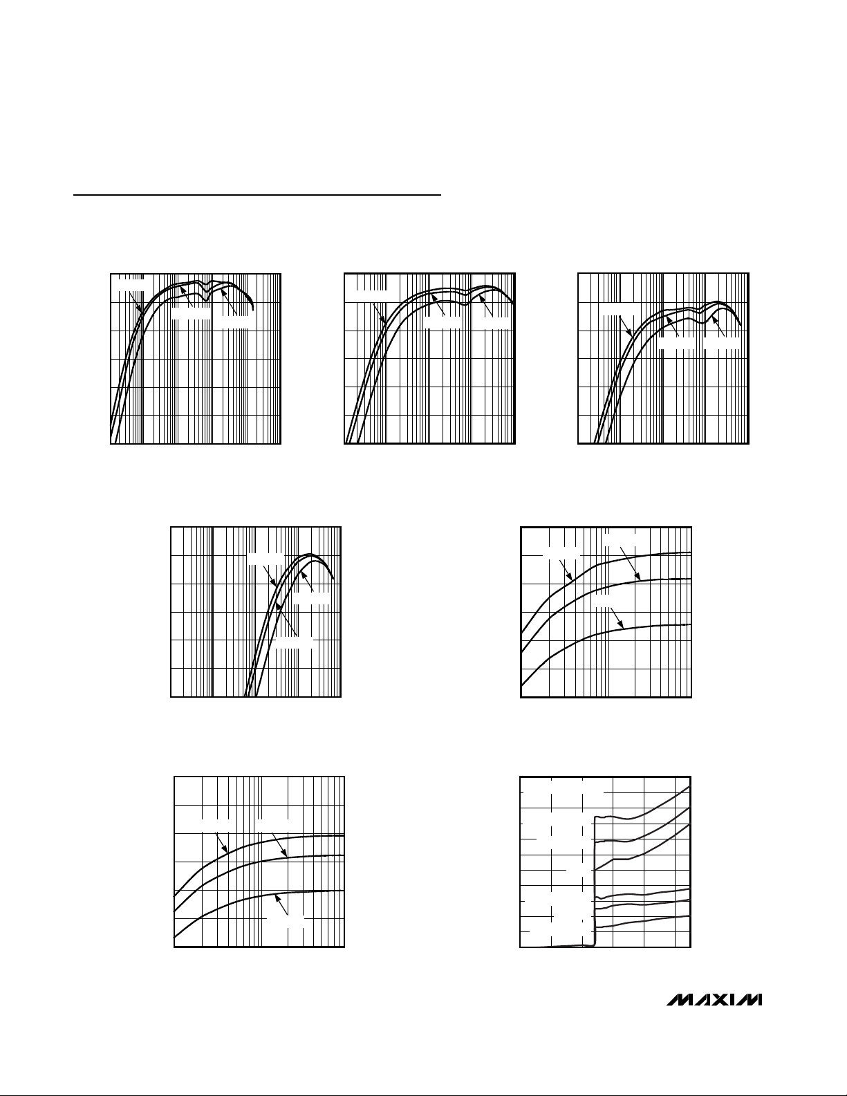
Typical Operating Characteristics
(Circuit of Figure 6, V
IN
= 3.6V, TA = +25°C, unless otherwise noted.)
100
0.1 1 10 100 1000 10,000
90
80
70
60
50
40
REG1 3.3V OUTPUT EFFICIENCY
vs. LOAD CURRENT
MAX8588 toc01
LOAD CURRENT (mA)
EFFICIENCY (%)
VIN = 3.6V
VIN = 4.0V
VIN = 5.0V
100
40
0.1 10 1001 1000
REG2 2.5V OUTPUT EFFICIENCY
vs. LOAD CURRENT
MAX8588 toc02
LOAD CURRENT (mA)
EFFICIENCY (%)
50
60
70
80
90
VIN = 3.6V
VIN = 4.0V
VIN = 5.0V
100
40
0.1 10 1001 1000
REG3 1.3V OUTPUT EFFICIENCY
vs. LOAD CURRENT
MAX8588 toc03
LOAD CURRENT (mA)
EFFICIENCY (%)
50
60
70
80
90
VIN = 3.6V
VIN = 4.0V VIN = 5.0V
0.1 10 1001 1000
REG3 1.3V OUTPUT WITH FORCED-PWM
EFFICIENCY vs. LOAD CURRENT
MAX8588 toc04
LOAD CURRENT (mA)
EFFICIENCY (%)
VIN = 3.6V
VIN = 5.0V
VIN = 4.0V
100
40
50
60
70
80
90
REG2 SLEEP LDO 2.5V OUTPUT
EFFICIENCY vs. LOAD CURRENT
MAX8588 toc06
LOAD CURRENT (mA)
EFFICIENCY (%)
90
30
40
50
60
70
80
0.1 1 10
VIN = 3.6V VIN = 4.0V
VIN = 5.0V
REG1 SLEEP LDO 3.3V OUTPUT
EFFICIENCY vs. LOAD CURRENT
MAX8588 toc05
LOAD CURRENT (mA)
EFFICIENCY (%)
100
40
50
60
70
80
90
0.1 1 10
VIN = 3.6V
VIN = 4.0V
VIN = 5.0V
0
20
140
100
180
220
021345
QUIESCENT CURRENT
vs. SUPPLY VOLTAGE
MAX8588 toc07
INPUT VOLTAGE (V)
INPUT CURRENT (µA)
BKBT BIASED AT 3.6V
V1, V2, AND V3 ON
V1 AND V2 ON
V1 ON
V1 AND V2 SLEEP
V1 SLEEP
ALL BUT V7 OFF
200
160
40
60
80
120
Page 11

MAX8588
High-Efficiency, Low-I
Q
PMIC with
Dynamic Core for PDAs and Smartphones
______________________________________________________________________________________ 11
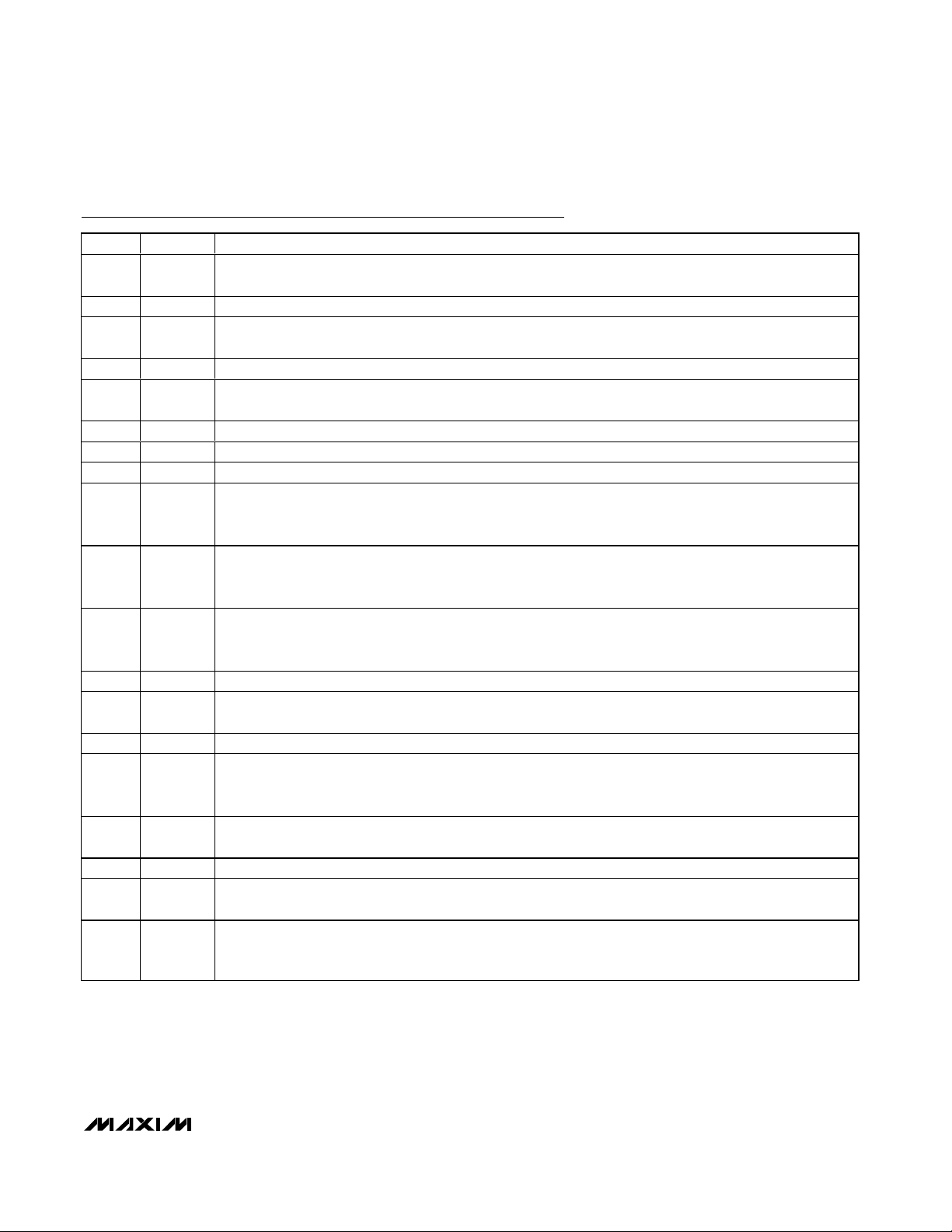
Typical Operating Characteristics (continued)
(Circuit of Figure 6, V
IN
= 3.6V, TA = +25°C, unless otherwise noted.)
300
250
200
150
100
DROPOUT VOLTAGE (mV)
50
1040
1000
960
920
SWITCHING FREQUENCY (kHz)
880
DROPOUT VOLTAGE
vs. LOAD CURRENT
MAX8588 toc08
REG1 3.3V OUTPUT
0
0 400200 600 800 1000 1200
LOAD CURRENT (mA)
SWITCHING FREQUENCY
vs. SUPPLY VOLTAGE
TA = +85°C
TA = +25°C
TA = -40°C
2.5 3.53.0 4.0 4.5 5.0 5.5
INPUT VOLTAGE (V)
MAX8588 toc10
CHANGE IN OUTPUT VOLTAGE
vs. LOAD CURRENT
200
150
100
50
0
-50
CHANGE IN OUTPUT VOLTAGE (mV)
-100
REG1 3.3V OUTPUT
REG2 2.5V OUTPUT
REG3 1.3V OUTPUT
VIN = 3.6V
0400200 600 800 1000 1200
LOAD CURRENT (mA)
REFERENCE VOLTAGE
vs. TEMPERATURE
1.265
1.260
1.255
1.250
1.245
1.240
1.235
REFERENCE VOLTAGE (V)
1.230
1.225
-40 -15 10 35 60 85
TEMPERATURE (°C)
MAX8588 toc09
MAX8588 toc11
REG1 SWITCHING WAVEFORMS
WITH 800mA LOAD
V1
V
LX1
I
L1
400ns/div
MAX8588 toc12
10mv/div
AC-COUPLED
2V/div
0
500mA/div
0
V
REG1 SWITCHING WAVEFORMS
WITH 10mA LOAD
V1
LX1
I
L1
20µs/div
MAX8588 toc13
50mv/div
AC-COUPLED
2V/div
0
500mA/div
0
Page 12

MAX8588
High-Efficiency, Low-IQPMIC with
Dynamic Core for PDAs and Smartphones
12 ______________________________________________________________________________________
Typical Operating Characteristics (continued)
(Circuit of Figure 6, V
IN
= 3.6V, TA = +25°C, unless otherwise noted.)
REG3 SWITCHING WAVEFORMS
WITH 250mA LOAD
MAX8588 toc14
REG3 PULSE-SKIP SWITCHING
WAVEFORMS WITH 10mA LOAD
MAX8588 toc15
V3
V
LX3
I
L3
V3
V
LX3
I
L3
400ns/div
REG3 FORCED-PWM SWITCHING
WAVEFORMS WITH 10mA LOAD
MAX8588 toc16
10mv/div
AC-COUPLED
2V/div
0
500mA/div
0
10mv/div
AC-COUPLED
2V/div
0V
500mA/div
0mA
V
RSO
V3
LX3
I
L3
10µs/div
10mv/div
AC-COUPLED
2V/div
0
500mA/div
0
V7 AND RSO
STARTUP WAVEFORMS
V
IN
V7
MAX8588 toc17
2V/div
0V
2V/div
0V
2V/div
0V
SYS_EN STARTUP WAVEFORMS
V
EN1
AND
V
EN2
V1
V2
V
POK
400ns/div
2ms/div
MAX8588 toc18
2V/div
2V/div
2V/div
2V/div
PWR_EN STARTUP WAVEFORMS
V
EN3
AND
V
EN45
V3
V4
V5
V
POK
10ms/div
MAX8588 toc19
1ms/div
2V/div
2V/div
2V/div
2V/div
2V/div
Page 13

MAX8588
High-Efficiency, Low-I
Q
PMIC with
Dynamic Core for PDAs and Smartphones
______________________________________________________________________________________ 13
Typical Operating Characteristics (continued)
(Circuit of Figure 6, V
IN
= 3.6V, TA = +25°C, unless otherwise noted.)
REG1 LOAD-TRANSIENT RESPONSE
200µs/div
REG3 LOAD-TRANSIENT RESPONSE
MAX8588 toc20
MAX8588 toc22
V1
100mV/div
AC-COUPLED
I
LOAD1
200mA/div
0A
V3
100mV/div
AC-COUPLED
I
LOAD3
200mA/div
REG2 LOAD-TRANSIENT RESPONSE
200µs/div
MAX8588 toc21
REG3 OUTPUT VOLTAGE CHANGING FROM
1.3V TO 1.0V WITH DIFFERENT VALUES OF C
C
= 2200pF
RAMP
C
= 1500pF
RAMP
C
= 1000pF
RAMP
MAX8588 toc23
V2
100mV/div
AC-COUPLED
I
LOAD2
200mA/div
0A
RAMP
C
= 330pF
RAMP
200µs/div
200µs/div
2.5V TO 3.0V
1.8V TO 2.5V
0 TO 1.8V
0A
REG6 USIM TRANSITIONS
V6
V6
V6
10µs/div
MAX8588 toc24
500mV/div
0
Page 14

MAX8588
High-Efficiency, Low-IQPMIC with
Dynamic Core for PDAs and Smartphones
14 ______________________________________________________________________________________
Pin Description
PIN NAME FUNCTION
1 LBI
Dual-Mode™, Low-Battery Input. Connect to IN to set the low-battery threshold to 3.6V (no resistors needed).
Connect LBI to a resistor-divider for an adjustable LBI threshold. When IN is below the set threshold, LBO
output switches low. LBO is deactivated and forced low when IN is below the dead-battery (DBI) threshold
and when all REGs are disabled.
2 CC1
REG1 Compensation Node. Connect a series resistor and capacitor from CC1 to GND to compensate the
regulation loop. See the Compensation and Stability section.
3 FB1
REG1 Feedback Input. Connect FB1 to GND to set V1 to 3.3V. Connect FB1 to external feedback resistors
for other output voltages.
4 BKBT Input Connection for Backup Battery. This input can also accept the output of an external boost converter.
5V7
Also known as VCC_BATT. V7 is always active if main or backup power is present. It is the first regulator that
powers up. V7 has two states:
1) V7 tracks V1 if ON1 is high and V1 is in regulation.
2) V7 tracks V
BKBT
when ON1 is low or V1 is out of regulation.
6V1
REG1 Voltage-Sense Input. Connect directly to the REG1 output voltage. The output voltage is set by FB1 to
either 3.3V or adjustable with resistors.
7 SLPIN Inp ut to V 1 and V 2 S l eep Re g ul ator s. The i np ut to the stand b y r eg ul ator s at V 1 and V 2. C onnect S LP IN to IN .
8V2
REG2 Voltage-Sense Input. Connect directly to the REG2 output voltage. The output voltage is set by FB2 to
either 3.3V/2.5V or adjustable with resistors.
9 FB2
REG2 Feedback Input. Connect to GND to set V2 to 2.5V on all devices. Connect FB2 to IN to set V2 to 3.3V.
Connect FB2 to external feedback resistors for other voltages.
10 CC2
REG2 Compensation Node. Connect a series resistor and capacitor from CC2 to GND to compensate the
regulation loop. See the Compensation and Stability section.
11 POK
Power-OK Output. Open-drain output that is low when any of the V1–V6 outputs are below their regulation
threshold. When all activated outputs are in regulation, POK is high impedance. POK maintains a valid low
output with V7 as low as 1V. POK does not flag an out-of-regulation condition while REG3 is transitioning
between voltages set by serial programming. POK also does not flag for any REG channel that has been
turned off; however, if all REG channels are off (V1–V6), then POK is forced low. If IN < UVLO, then POK is
low. POK is expected to connect to nVCC_FAULT.
12 SCL Serial Clock Input
13 SDA
Serial Data Input. Serial data programs the REG3 (core) and REG6 (VCC_USIM) voltage. REG3 and REG6
can be programmed even when off, but at least one of the ON_ pins must be logic-high to activate the serial
interface. On power-up, REG3 defaults to 1.3V and REG6 defaults to 0V.
14 PWM3
Force V3 to PWM at All Loads. Connect PWM3 to GND for normal operation (skip mode at light loads). Drive
or connect high for forced-PWM operation at all loads for V3 only.
15 LBO Low-Battery Output. Open-drain output that goes low when IN is below the threshold set by LBI.
Dual Mode is a trademark of Maxim Integrated Products, Inc.
Page 15
MAX8588
High-Efficiency, Low-I
Q
PMIC with
Dynamic Core for PDAs and Smartphones
______________________________________________________________________________________ 15
Pin Description (continued)
PIN NAME FUNCTION
16 PV2
REG2 Power Input. Bypass to PG2 with a 4.7µF or greater low-ESR capacitor. PV1, PV2, PV3, and IN must
connect together externally.
17 LX2 REG2 Switching Node. Connects to REG2 inductor.
18 PG2
REG2 Power Ground. Connect directly to a power-ground plane. Connect PG1, PG2, PG3, and GND
together at a single point as close to the IC as possible.
19 IN Main Battery Input. This input provides power to the IC.
20 RAMP
V3 Ramp-Rate Control. A capacitor connected from RAMP to GND sets the rate-of-change when V3 is
changed. The output impedance of RAMP is 100kΩ. FB3 regulates to 1.28 x V
RAMP
.
21 GND Analog Ground
22 REF Reference Output. Output of the 1.25V reference. Bypass to GND with a 0.1µF or greater capacitor.
23 BYP Low-Noise LDO Bypass. Low-noise bypass pin for V4 LDO. Connect a 0.01µF capacitor from BYP to GND.
24 DBO
Dead or Missing Battery Output. DBO is an open-drain output that goes low when IN is below the threshold
set by DBI. DBO does not deactivate any regulator outputs. DBO is expected to connect to nBATT_FAULT
on Intel CPUs.
25 ON2
On/Off Input for REG2. Drive high to turn on. When enabled, the REG2 output soft-starts. ON2 has hysteresis
so an RC can be used to implement manual sequencing with respect to other inputs. It is expected that ON1,
ON2, and ON6 are connected to SYS_EN.
26 ON4
On/Off Input for REG4. Drive high to turn on. When enabled, the REG4 output activates. ON4 has hysteresis
so an RC can be used to implement manual sequencing with respect to other inputs. It is expected that ON4
is connected to PWR_EN.
27 V4 Also Known as VCC_PLL. 1.3V, 35mA linear-regulator output for PLL. Regulator input is IN45.
28 IN45
Power Input to V4 and V5 LDOs. Typically connected to V2, but can also connect to IN or another voltage
from 2.5V to V
IN
.
29 V5 Also Known as VCC_SRAM. 1.1V, 35mA linear-regulator output for CPU SRAM. Regulator input is IN45.
30 ON5
On/Off Input for REG5. Drive high to turn on. When enabled, the MAX8588 soft-starts the REG5 output. ON5
has hysteresis so an RC can be used to implement manual sequencing with respect to other inputs. It is
expected that ON5 is connected to PWR_EN.
31 PG3
REG3 Power Ground. Connect directly to a power-ground plane. Connect PG1, PG2, PG3, and GND
together at a single point as close to the IC as possible.
32 LX3 REG3 Switching Node. Connects to the REG3 inductor.
33 PV3
REG3 Power Input. Bypass to PG3 with a 4.7µF or greater low-ESR ceramic capacitor. PV1, PV2, PV3, and IN
must connect together externally.
34 ON3
On/Off Input for REG3 (Core). Drive high to turn on. When enabled, the REG3 output ramps up. ON3 has
hysteresis so an RC can be used to implement manual sequencing with respect to other inputs. It is
expected that ON3 is driven from CPU SYS_EN.
Page 16

MAX8588
High-Efficiency, Low-IQPMIC with
Dynamic Core for PDAs and Smartphones
16 ______________________________________________________________________________________
Pin Description (continued)
PIN NAME FUNCTION
35 SRAD
Serial Address Bit. SRAD allows the serial address to be changed in case it conflicts with another serial
device. If SRAD = GND, A1 = 0. If SRAD = IN, A1 = 1.
36 RSO
Open-Drain Reset Output. Deasserts when V7 exceeds 2.55V (typ rising). Has 65ms delay before release.
RSO is expected to connect to nRESET on the CPU.
37 MR
Manual Reset Input. A low input at MR causes the RSO output to go low and also resets the V3 output to its
default 1.3V setting. MR impacts no other functions.
38 CC3
REG 3 Compensation Node. Connect a series resistor and capacitor from CC3 to GND to compensate the
regulation loop. See the Compensation and Stability section.
39 FB3
REG3 Feedback-Sense Input. Connect directly to the REG3 output voltage. Output voltage is set by the serial
interface.
40 ON6
On/Off Input for REG6. Drive high to turn on. When enabled, the REG6 output activates. ON6 has hysteresis
so an RC can be used to implement manual sequencing with respect to other inputs. It is expected that ON1,
ON2, and ON6 are connected to SYS_EN.
41 V6
Also known as VCC_USIM. Linear-regulator output. This voltage is programmable through the I
2
C interface to
0V, 1.8V, 2.5V, or 3.0V. The default voltage is 0V. REG6 is activated when ON6 is high.
42 IN6 Power Input to the V6 LDO. Typically connected to V1, but can also connect to IN.
43 PG1
REG1 Power Ground. Connect directly to a power-ground plane. Connect PG1, PG2, PG3, and GND
together at a single point as close to the IC as possible.
44 LX1 REG1 Switching Node. Connects to the REG1 inductor.
45 PV1
REG1 Power Input. Bypass to PG2 with a 4.7µF or greater low-ESR ceramic capacitor. PV1, PV2, PV3, and IN
must connect together externally.
46 ON1
On/Off Input for REG1. Drive high to turn on REG1. When enabled, the REG1 output soft-starts. ON1 has
hysteresis so an RC can be used to implement manual sequencing with respect to other inputs. It is
expected that ON1, ON2, and ON6 connect to SYS_EN.
47 SLP
Sleep Input. SLP selects which regulators ON1 and ON2 turn on. SLP = high is normal operation (ON1 and
ON2 are the enables for the V1 and V2 DC-DC converters). SLP = low is sleep operation (ON1 and ON2 are
the enables for the V1 and V2 LDOs).
48 DBI
Dual-Mode, Dead-Battery Input. Connect DBI to IN to set the dead-battery falling threshold to 3.15V (no
resistors needed). Connect DBI to a resistor-divider for an adjustable DBI threshold.
EP EP
Exposed Metal Pad. Connect the exposed pad to ground. Connecting the exposed pad to ground does not
remove the requirement for proper ground connections to the appropriate ground pins.
Purchase of I2C components from Maxim Integrated Products, Inc. or one of its sublicensed Associated Companies, conveys a
license under the Philips I
2
C Patent Rights to use these components in an I2C system, provided that the system conforms to the I2C
Standard Specification as defined by Philips.
Page 17
MAX8588
High-Efficiency, Low-I
Q
PMIC with
Dynamic Core for PDAs and Smartphones
______________________________________________________________________________________ 17
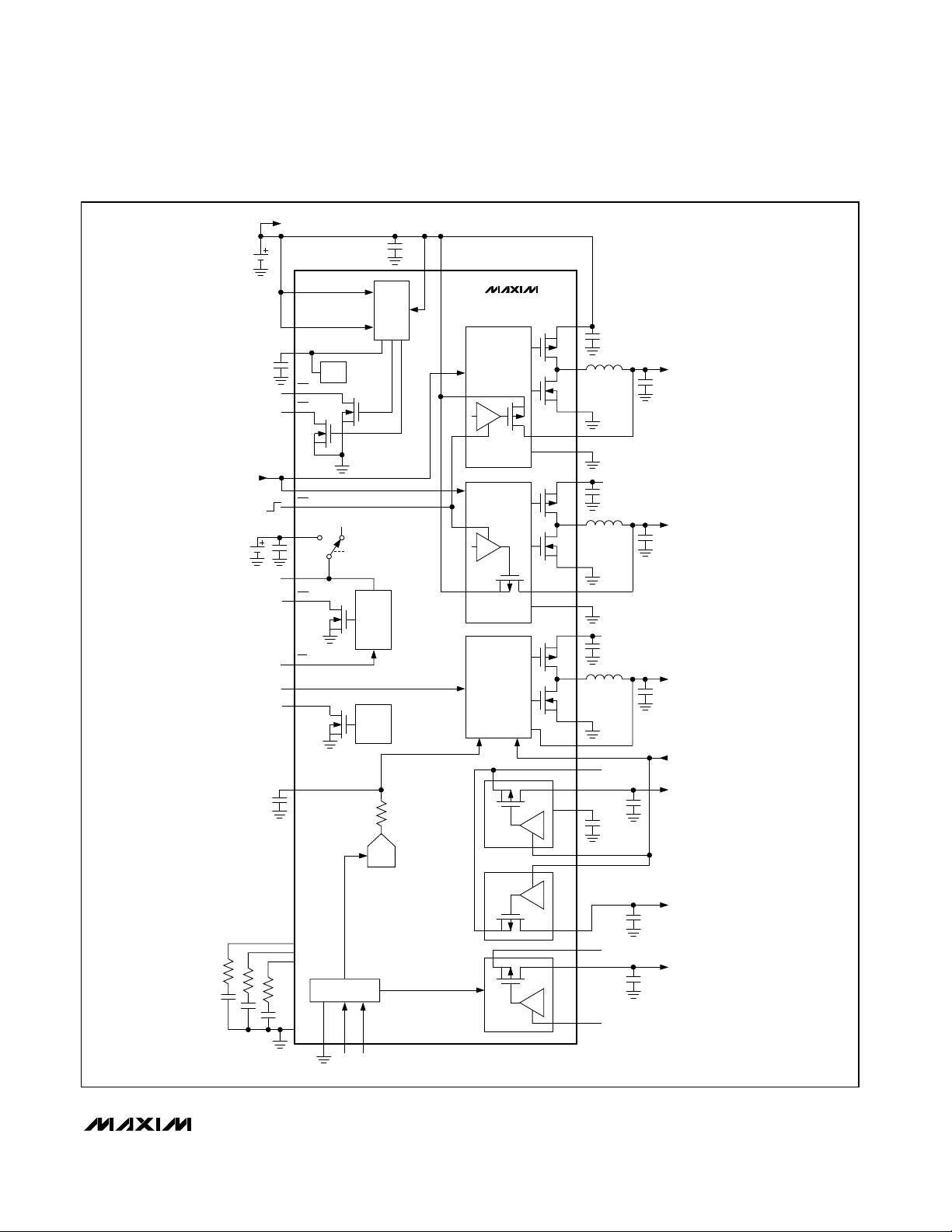
Figure 1. MAX8588 Functional Diagram
MAIN
BATT
OPEN-DRAIN LOW-BATT OUT
OPEN-DRAIN DEAD-BATT OUT
TO nBATT_FAULT
FROM CPU
SYS_EN
RUN
SLEEP
Li+
BACKUP
BATTERY
V7, VCC_BATT
(1ST SUPPLY, ALWAYS ON)
TO CPU
nRESET
RESET INPUT
FORCE REG3
TO PWM
TO CPU
nVCC_FAULT
BATT
DBI (3.15V OR ADJ)
LBI (3.6V OR ADJ)
REF
LBO
DBO
ON1
ON2
SLP
BKBT
V7
RSO
MR
PWM3
POK
RAMP
CC1
CC2
CC3
GND
REF
1.25V
SRAD
TO V1
2
I
SERIAL
REG1 OK
V1–V6
POWER-
C
SCL SDA
V7
RESET
2.425V
65ms
OK
DAC
SLPININ
UVLO
AND
BATT
MON
100kΩ
V3
MAX8588
STEP-DOWN
PWM
REG1
ON
SLEEP
LDO
ON
STEP-DOWN
PWM
REG2
SLEEP
LDO
STEP-DOWN
PWM
REG3
PWM
ADJ ON
LDO
REG
4
LDO
REG
5
LDO
REG
6
PV1
LX1
PG1
V1
FB1
PV2
TO BATT
LX2
PG2
V2
FB2
PV3
TO BATT
LX3
PG3
FB3
ON3
IN45
TO V2
V4
BYP
ON4
ON5
V5
IN6
TO V2
V6
ON6
FROM CPU
SYS_EN
V1, VCC_IO
3.3V WITH FB1 = GND,
OR ADJ WITH RESISTORS
V2, VCC_MEM
2.5V WITH FB2 = GND,
3.3V WITH FB2 = IN
OR ADJ WITH RESISTORS
V3, VCC_CORE
0.7V TO 1.475V
500mA
FROM CPU
PWR_EN
V4, VCC_PLL
1.3V, 35mA
V5, VCC_SRAM
1.1V, 35mA
VCC_USIM
0V, 1.8V, 3.0V (DEF = 0V)
Page 18

MAX8588
High-Efficiency, Low-IQPMIC with
Dynamic Core for PDAs and Smartphones
18 ______________________________________________________________________________________
Detailed Description
The MAX8588 power-management IC is optimized for
devices using Intel X-Scale microprocessors, including
third-generation smart cell phones, PDAs, internet
appliances, and other portable devices requiring substantial computing and multimedia capability at low
power. The MAX8588 complies with Intel Processor
Power specifications.
The IC integrates seven high-performance, low-operating-current power supplies along with supervisory and
management functions. Regulator outputs include three
step-down DC-DC outputs (V1, V2, and V3), three linear regulators (V4, V5, and V6), and one always-on output, V7 (Intel VCC_BATT). The V1 step-down DC-DC
converter provides 3.3V or adjustable output voltage for
I/O and peripherals. The V2 step-down DC-DC converter is preset for 3.3V or 2.5V. V2 can also be adjusted
with external resistors on all parts. The V3 step-down
DC-DC converter provides a serial-programmed output
for powering microprocessor cores. The three linear
regulators (V4, V5, and V6) provide power for PLL,
SRAM, and USIM.
To minimize sleep-state quiescent current, V1 and V2
have bypass “sleep” LDOs that can be activated to
minimize battery drain when output current is very low.
Other functions include separate on/off control for all
DC-DC converters, low-battery and dead-battery
detection, a power-OK output, a backup-battery input,
and a two-wire serial interface.
All DC-DC outputs use fast, 1MHz PWM switching and
small external components. They operate with fixed-frequency PWM control and automatically switch from
PWM to skip-mode operation at light loads to reduce
operating current and extend battery life. The V3 core
output is capable of forced-PWM operation at all loads.
The 2.6V to 5.5V input voltage range allows 1-cell Li+,
3-cell NiMH, or a regulated 5V input.
The following power-supply descriptions include the
Intel terms for the various voltages in parenthesis. For
example, the V1 output is referred to as VCC_IO in Intel
documentation. See Figure 1.
V1 and V2 (VCC_IO, VCC_MEM)
Step-Down DC-DC Converters
V1 is a 1MHz current-mode step-down converter. The V1
output voltage can be preset to 3.3V or adjusted using a
resistor voltage-divider. V1 supplies loads up to 1300mA.
V2 is also a 1MHz current-mode step-down converter.
The V2 step-down DC-DC converter is preset for 3.3V
or 2.5V. V2 can also be adjusted with external resistors
on all parts. V2 supplies loads up to 900mA.
Under moderate to heavy loading, the converters operate
in a low-noise PWM mode with constant frequency and
modulated pulse width. Switching harmonics generated
by fixed-frequency operation are consistent and easily filtered. Efficiency is enhanced under light loading (<30mA
typ), by assuming an Idle Mode™ during which the converter switches only as needed to service the load.
Synchronous Rectification
Internal n-channel synchronous rectifiers eliminate the
need for external Schottky diodes and improve efficiency. The synchronous rectifier turns on during the second half of each cycle (off-time). During this time, the
voltage across the inductor is reversed, and the inductor current falls. In normal operation (not forced PWM),
the synchronous rectifier turns off at the end of the
cycle (at which time another on-time begins) or when
the inductor current approaches zero.
100% Duty-Cycle Operation
If the inductor current does not rise sufficiently to supply the load during the on-time, the switch remains on,
allowing operation up to 100% duty cycle. This allows
the output voltage to maintain regulation while the input
voltage approaches the regulation voltage. Dropout
voltage is approximately 180mV for an 800mA load on
V1 and 220mV for an 800mA load on V2. During
dropout, the high-side p-channel MOSFET turns on,
and the controller enters a low-current-consumption
mode. The device remains in this mode until the regulator channel is no longer in dropout.
Sleep LDOs
In addition to the high-efficiency step-down converters,
V1 and V2 can also be supplied with low-quiescent current, low-dropout (LDO) linear regulators that can be
used in sleep mode or at any time when the load current
is very low. The sleep LDOs can source up to 35mA. To
enable the sleep LDOs, drive SLP low. When SLP is high,
the switching step-down converters are active. The output voltage of the sleep LDOs is set to be the same as
the switching step-down converters as described in the
Setting the Output Voltages section. SLPIN is the input to
the V1 and V2 sleep LDOs and must connect to IN.
Idle Mode is a trademark of Maxim Integrated Products, Inc.
Page 19

MAX8588
High-Efficiency, Low-I
Q
PMIC with
Dynamic Core for PDAs and Smartphones
______________________________________________________________________________________ 19
V3 (VCC_CORE) Step-Down
DC-DC Converter
V3 is a 1MHz current-mode step-down converter. It supplies loads up to 500mA.
The V3 output is set by the I2C serial interface to
between 0.7V and 1.475V in 25mV increments. The
default output voltage on power-up, and after a reset, is
1.3V. See the Serial Interface section for programming
details. See the Applications Information for instructions
on how to increase the V3 output voltage.
Forced PWM on REG3
Under moderate to heavy loading, the V3 always operates
in a low-noise PWM mode with constant frequency and
modulated pulse width. Switching harmonics generated by
fixed-frequency operation are consistent and easily filtered.
With light loads (<30mA) and PWM3 low, V3 operates
in an enhanced-efficiency idle mode during which the
converter switches only as needed to service the load.
With PWM3 high, V3 operates in low-noise forced-PWM
mode under all load conditions.
Linear Regulators (V4, V5, and V6)
V4 (VCC_PLL)
V4 is a linear regulator that provides a fixed 1.3V output
and supplies loads up to 35mA. The power input for the
V4 and V5 linear regulators is IN45, which is typically
connected to V2. To enable V4, drive ON4 high, or drive
ON4 low for shutdown. V4 is intended to connect to
VCC_PLL.
V5 (VCC_SRAM)
V5 is a linear regulator that provides a fixed 1.1V output
and supplies loads up to 35mA. The power input for the
V4 and V5 linear regulators is IN45, which is typically
connected to V2. To enable V5, drive ON5 high, or drive
ON5 low for shutdown. V5 is intended to connect to
VCC_SRAM.
V6 (VCC_USIM)
V6 is a linear regulator that supplies loads up to 35mA.
The V6 output voltage is programmed with the I2C serial interface to 0V, 1.8V, 2.5V, or 3.0V. The power-up
default for V6 is 0V. See the Serial Interface section for
details on changing the voltage. The power input for the
V6 linear regulator is IN6, which is typically connected
to V1. To enable V6, drive ON6 high, or drive ON6 low
for shutdown. V6 is intended to connect to VCC_USIM.
V7 Always-On Output (VCC_BATT)
The V7 output is always active if V1 is enabled and in
regulation or if backup power is present. When ON1 is
high and V1 is in regulation, V7 is sourced from V1 by
an internal MOSFET switch. When ON1 is low or V1 is
out of regulation, V7 is sourced from BKBT by a second
on-chip MOSFET. V7 can supply loads up to 30mA. V7
is intended to connect to VCC_BATT on Intel CPUs.
Due to variations in system implementation, BKBT and
V7 can be utilized in different ways. See the Backup-
Battery Configurations section for information on how to
use BKBT and V7.
Quiescent Operating Current
in Various States
The MAX8588 is designed for optimum efficiency and
minimum operating current for all typical operating
modes, including sleep and deep sleep. These states
are outlined in Table 1.
Table 1. Quiescent Operating Current in Various States
OPERATING
POWER MODE
RUN All supplies on and running.
IDLE All supplies on and running, peripherals on.
SENSE All supplies on, minimal loading, peripherals monitored.
STANDBY All supplies on, minimal loading, peripherals not monitored.
SLEEP P W R_E N contr ol l ed vol tag es ( V 3, V 4, V 5) ar e off. V 1 and V 2 on.
DEEP SLEEP All supplies off except V7. V7 biased from backup battery.
DESCRIPTION
TYPICAL NO-LOAD
OPERATING CURRENT
225µA
60µA if V1 and V2 SLEEP LDOs on;
130µA if V1, V2 step-down DC-DCs enabled
32µA if IN > DBI threshold;
4µA if IN < DBI threshold
Page 20
MAX8588
High-Efficiency, Low-IQPMIC with
Dynamic Core for PDAs and Smartphones
20 ______________________________________________________________________________________
Voltage Monitors, Reset, and
Undervoltage-Lockout Functions
Undervoltage Lockout
When the input voltage is below 2.35V (typ), an undervoltage-lockout (UVLO) circuit disables the IC. The
inputs remain high impedance while in UVLO, reducing
battery load under this condition. All serial registers are
maintained with the input voltage down to at least 2.35V.
Reset Output
(RSO)
and MRInput
The reset output (RSO) is low when the MR input is low
or when V7 is below 2.425V. V7 is powered from V1
(when enabled) or the backup-battery input (BKBT).
RSO normally goes low:
1) When power is first applied in configurations with no
separate backup battery (external diode from IN to
BKBT).
2) When power is removed in configurations with no
separate backup battery (external diode from IN to
BKBT).
3) If the backup battery falls below 2.425V when V1 is
off or out of regulation.
4) When the manual reset button is pressed (MR goes
low).
If VIN> 2.4V, an internal timer delays the release of RSO
for 65ms after V7 rises above 2.3V. However, if V
IN
<
2.4V when V7 exceeds 2.3V, or if VINand V7 rise at the
same time, RSO deasserts immediately with no 65ms
delay. There is no delay in the second case because the
timer circuitry is deactivated to minimize operating current during VINundervoltage lockout.
If it is desired to have a 65ms RSO release delay for any
sequence of VINand V7, the circuit in Figure 2 may be
used. An RC connected from IN to MR delays the rise of
MR until after VINpowers up. The 65ms timer is valid for
either sequence of V7 and VINand does not release until
65ms after both are up. The only regulator output that
affects RSO is V7. RSO will not respond to V1–V6, which
are monitored by POK. Also, RSO is high impedance
and does not function if BKBT is not powered.
MR is a manual reset input for hardware reset. A low
input at MR causes the RSO output to go low for at least
65ms and also resets the V3 output to its default 1.3V setting and turns off the V6 output. MR impacts no other
MAX8588 functions.
Dead-Battery and
Low-Battery Comparators—DBI, LBI
The DBI and LBI inputs monitor input power (usually a
battery) and trigger the DBO and LBO outputs. The
dead-battery comparator triggers DBO when the battery
(V
IN
) discharges to the dead-battery threshold. The
factory-set 3.15V threshold is selected by connecting
DBI to IN, or the threshold can be programmed with a
resistor-divider at DBI. The low-battery comparator has
a factory-set 3.6V threshold that is selected by connecting LBI to IN, or its threshold can be programmed with a
resistor-divider at LBI.
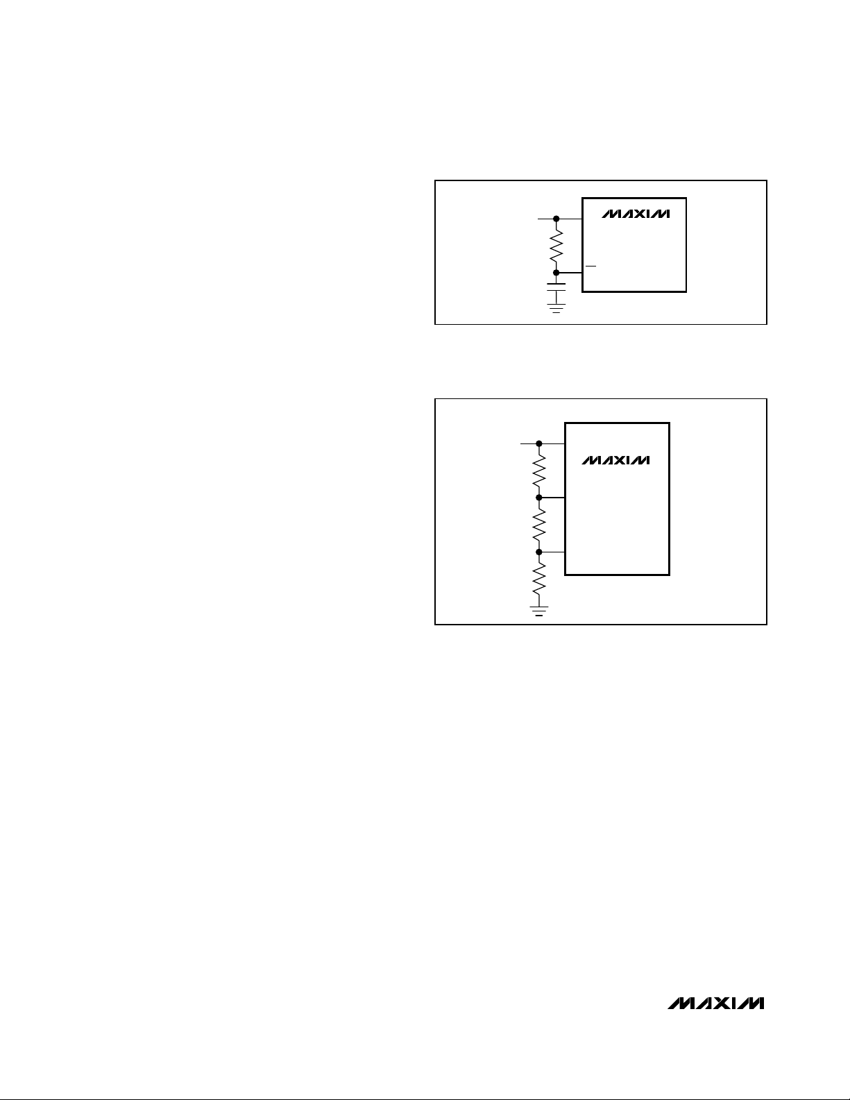
One three-resistor-divider can set both DBI and LBI
(R1, R2, and R3 in Figure 3) according to the following
equations:
1) Choose R3 to be less than 250kΩ
2) R1 = R3 VLB(1 - (1.232 / VDB))
3) R2 = R3 (1.232 x (V
LB
/ VDB) - 1)
where V
LB
is the low-battery threshold and VDBis the
dead-battery threshold.
Figure 3. Setting the Low-Battery and Dead-Battery Thresholds
with One Resistor Chain. The values shown set a DBI threshold
of 3.3V and an LBI threshold of 3.5V (no resistors are needed
for the factory preset thresholds).
Figure 2. An RC delay connected from IN to MRensures that
the 65ms
RSO
release delay remains in effect for any
sequence of IN and V7.
100kΩ
0.22µF
MAIN BATTERY
438kΩ
200kΩ
R1
R2
62kΩ
R3
IN
MAX8588
MR
IN
MAX8588
DBI (1.232V THRESHOLD)
LBI (1.00V THRESHOLD)
Page 21

MAX8588
High-Efficiency, Low-I
Q
PMIC with
Dynamic Core for PDAs and Smartphones
______________________________________________________________________________________ 21
Alternately, LBI and DBI can be set with separate tworesistor-dividers. Choose the lower resistor of the divider
chain to be 250kΩ or less (R5 and R7 in Figure 4). The
equations for upper divider-resistors as a function of
each threshold are then:
R4 = R5 (V
DB
/ 1.232) - 1)
R6 = R7 (VLB- 1)
When resistors are used to set VLB, the threshold at LBI
is 1.00V. When resistors are used to set VDB, the
threshold at DBI is 1.232V. A resistor-set threshold can
also be used for only one of DBI or LBI. The other
threshold can then be factory set by connecting the
appropriate input to IN.
If BKBT is not powered, DBO does not function and is
high impedance. DBO is expected to connect to
nBATT_FAULT on Intel CPUs. If BKBT is not powered,
LBO does not function and is high impedance.
Power-OK Output (POK)
POK is an open-drain output that goes low when any
activated regulator (V1–V6) is below its regulation
threshold. POK does not monitor V7. When all active
output voltages are within 10% of regulation, POK is
high impedance. POK does not flag an out-of-regulation condition while V3 is transitioning between voltages
set by serial programming or when any regulator channel has been turned off. POK momentarily goes low
when any regulator is turned on, but returns high when
that regulator reaches regulation. When all regulators
(V1–V6) are off, POK is forced low. If the input voltage
is below the UVLO threshold, POK is held low and
maintains a valid low output with IN as low as 1V. If
BKBT is not powered, POK does not function and is
high impedance.
Connection to Processor
and Power Sequencing
Typical processor connections have only power-control
pins, typically labeled PWR_EN and SYS_EN. The
MAX8588 provides numerous on/off control pins for
maximum flexibility. In a typical application, many of
these pins are connected together. ON1, ON2, and
ON6 typically connect to SYS_EN. ON3, ON4, and ON5
typically connect to PWR_EN. V7 remains on as long as
the main or backup power is connected. Sequencing is
not performed internally on the MAX8588; however, all
ON_ inputs have hysteresis and can connect to RC networks to set sequencing. For typical connections to Intel
CPUs, no external sequencing is required.
Backup-Battery Input
The backup-battery input (BKBT) provides backup
power for V7 when V1 is disabled. Normally, a primary
or rechargeable backup battery is connected to this
pin. If a backup battery is not used, then BKBT should
connect to IN through a diode or external regulator. See
the Backup-Battery Configurations section for informa-
tion on how to use BKBT and V7.
Serial Interface
An I2C-compatible, two-wire serial interface controls
REG3 and REG6. The serial interface operates when IN
exceeds the 2.40V UVLO threshold and at least one of
ON1–ON6 is asserted. The serial interface is shut down
to minimize off-current drain when no regulators are
enabled.
The serial interface consists of a serial data line (SDA)
and a serial clock line (SCL). Standard I2C-compatible
write-byte commands are used. Figure 4 shows a timing diagram for the I2C protocol. The MAX8588 is a
slave-only device, relying upon a master to generate a
clock signal. The master (typically a microprocessor)
initiates data transfer on the bus and generates SCL to
permit data transfer. A master device communicates to
the MAX8588 by transmitting the proper address followed by the 8-bit data code (Table 2). Each transmit
sequence is framed by a START (A) condition and a
STOP (L) condition. Each word transmitted over the bus
is 8 bits long and is always followed by an acknowledge clock pulse.
Table 2 shows the serial data codes used to program
V3 and V6. The default power-up voltage for V3 is 1.3V
and for V6 is 0V.
Figure 4. Setting the Low-Battery and Dead-Battery Thresholds
with Separate Resistor-Dividers. The values shown set a DBI
threshold of 3.3V and an LBI threshold of 3.5V (no resistors are
needed for factory-preset thresholds).
MAIN BATTERY
R4
334kΩ
R5
200kΩ
R6
500kΩ
R7
200kΩ
IN
MAX8588
DBI (1.232V THRESHOLD)
LBI (1.00V THRESHOLD)
Page 22

MAX8588
High-Efficiency, Low-IQPMIC with
Dynamic Core for PDAs and Smartphones
22 ______________________________________________________________________________________
Table 2. V3 and V6 Serial Programming Codes
D7 D6
XX
D5
0 = PROG V3
1 = PROG V6
0 000000.700
0 000010.725
0 000100.750
0 000110.775
0 001000.800
0 001010.825
0 001100.850
0 001110.875
0 010000.900
0 010010.925
0 010100.950
0 010110.975
0 011001.000
0 011011.025
0 011101.050
0 011111.075
0 100001.100
0 100011.125
0 100101.150
0 100111.175
0 101001.200
0 101011.225
0 101101.250
0 101111.275
0 110001.300
0 110011.325
0 110101.350
0 110111.375
0 111001.400
0 111011.425
0 111101.450
0 111111.475
1 XXX 0 0 0
1 XXX0 11.8
1 XXX1 02.5
1 XXX1 13.0
D4 D3 D2 D1 D0
OUTPUT
(V)
DESCRIPTION
V3, CORE
VOLTAGES
V6, USIM
VOLTAGES
Page 23

MAX8588
High-Efficiency, Low-I
Q
PMIC with
Dynamic Core for PDAs and Smartphones
______________________________________________________________________________________ 23
Bit Transfer
One data bit is transferred during each SCL clock
cycle. The data on SDA must remain stable during the
high period of the SCL clock pulse. Changes in SDA
while SCL is high are control signals (see the START
and STOP Conditions section). Both SDA and SCL idle
high when the bus is not busy.
START and STOP Conditions
When the serial interface is inactive, SDA and SCL idle
high. A master device initiates communication by issuing a START condition. A START condition is a high-tolow transition on SDA with SCL high. A STOP condition
is a low-to-high transition on SDA while SCL is high
(Figure 5). A START condition from the master signals
the beginning of a transmission to the MAX8588. The
master terminates transmission by issuing a not
acknowledge followed by a STOP condition (see the
Acknowledge Bit section). The STOP condition frees
the bus.
When a STOP condition or incorrect address is detected, the MAX8588 internally disconnects SCL from the
serial interface until the next START condition, minimizing digital noise and feedthrough.
Acknowledge Bit (ACK)
The acknowledge bit (ACK) is the ninth bit attached to
every 8-bit data word. The receiving device always
generates ACK. The MAX8588 generates an ACK when
receiving an address or data by pulling SDA low during
the ninth clock period. Monitoring ACK allows for
detection of unsuccessful data transfers. An unsuccessful data transfer occurs if a receiving device is
busy or if a system fault has occurred. In the event of
an unsuccessful data transfer, the bus master should
reattempt communication at a later time.
Serial Address
A bus master initiates communication with a slave
device by issuing a START condition followed by the
7-bit slave address (Table 3). When idle, the MAX8588
waits for a START condition followed by its slave
address. The serial interface compares each address
value bit by bit, allowing the interface to power down
immediately if an incorrect address is detected.
The LSB of the address word is the read/write (R/W) bit.
R/W indicates whether the master is writing or reading
(RD/W 0 = write, RD/W 1 = read). The MAX8588 only
supports the SEND BYTE format; therefore, RD/W is
required to be 0.
After receiving the proper address, the MAX8588
issues an ACK by pulling SDA low for one clock cycle.
The MAX8588 has two user-programmed addresses
(Table 3). Address bits A6 through A1 are fixed, while
A1 is controlled by SRAD. Connecting SRAD to GND
sets A1 = 0. Connecting ADD to IN sets A1 = 1.
V3 Output Ramp-Rate Control
When V3 is dynamically changed with the serial interface, the output voltage changes at a rate controlled by
a capacitor (C
RAMP
) connected from RAMP to ground.
The voltage change is a conventional RC exponential
described by:
Vo(t) = Vo(0) + dV(1 – exp(-t / (100kΩ C
RAMP
)))
Figure 5. I2C-Compatible Serial-Interface Timing Diagram
Table 3. Serial Address
AB CDEFG HIJK
t
LOWtHIGH
SCL
SDA
t
t
HD:STA
SU:STA
A = START CONDITION
B = MSB OF ADDRESS CLOCKED INTO SLAVE
C = LSB OF ADDRESS CLOCKED INTO SLAVE
D = R/W BIT CLOCKED INTO SLAVE
E = SLAVE PULLS SMB DATA LINE LOW
t
SU:DAT
F = ACKNOWLEDGE BIT CLOCKED INTO MASTER
G = MSB OF DATA CLOCKED INTO SLAVE (OP/SUS BIT)
H = LSB OF DATA CLOCKED INTO SLAVE
I = SLAVE PULLS SMB DATA LINE LOW
L M
t
HD:DAT
J = ACKNOWLEDGE CLOCKED INTO MASTER
K = ACKNOWLEDGE CLOCK PULSE
L = STOP CONDITION, DATA EXECUTED BY SLAVE
M = NEW START CONDITION
t
SU:STO
t
BUF
SRAD A7 A6 A5 A4 A3 A2 A1
0 0010100 0
1 0010101 0
A0
RD/W
Page 24

MAX8588
High-Efficiency, Low-IQPMIC with
Dynamic Core for PDAs and Smartphones
24 ______________________________________________________________________________________
A useful approximation is that it takes approximately 2.2
RC time constants for V3 to move from 10% to 90% of
the voltage difference. For C
RAMP
= 1500pF, this time
is 330µs. For a 1V to 1.3V change, this equates to
1mV/µs. See the Typical Operating Characteristics for
examples of different ramp-rate settings.
The maximum capacitor value that can be used at
RAMP is 2200pF. If larger values are used, the V3 ramp
rate is still controlled according to the above equation,
but when V3 is first activated, POK indicates an “in regulation” condition before V3 reaches its final voltage.
The RAMP pin is effectively the reference for REG3.
FB3 regulates to 1.28 times the voltage on RAMP.
Design Procedure
Setting the Output Voltages
The outputs V1 and V2 have preset output voltages, but
can also be adjusted using a resistor voltage-divider. To
set V1 to 3.3V, connect FB1 to GND. V2 can be preset to
3.3V or 2.5V. To set V2 to 3.3V, connect FB2 to IN. To set
to 2.5V, connect FB2 to GND.
To set V1 or V2 to other than the preset output voltages,
connect a resistor voltage-divider from the output voltage to the corresponding FB input. The FB_ input bias
current is less than 100nA, so choose the low-side (FB_to-GND) resistor (RL) to be 100kΩ or less. Then calculate the high-side (output-to-FB_) resistor (RH) using:
RH= RL[(V
OUT
/ 1.25) – 1]
The V3 (VCC_CORE) output voltage is set from 0.7V to
1.475V in 25mV steps by the I2C serial interface. See
the Serial Interface section for details.
Linear regulator V4 provides a fixed 1.3V output voltage. Linear regulator V5 provides a fixed 1.1V output
voltage. V4 and V5 voltages are not adjustable.
The output voltage of linear regulator V6 (VCC_USIM) is
set to 0V, 1.8V, 2.5V, or 3.0V by the I2C serial interface.
See the Serial Interface section for details.
Linear regulator V7 (VCC_BATT) tracks the voltage at
V1 as long as ON1 is high and V1 is in regulation. When
ON1 is low or V1 is not in regulation, V7 switches to the
backup battery (V
BKBT
).
Inductor Selection
The external components required for the step-down
are an inductor, input-and-output filter capacitors, and
a compensation RC network.
The MAX8588 step-down converter provides its best
efficiency with continuous inductor current. A reasonable inductor value (L
IDEAL
) is derived from:
L
IDEAL
= [2(VIN) x D(1 - D)] / (I
OUT(MAX)
x f
OSC
)
This sets the peak-to-peak inductor current at 1/2 the
DC inductor current. D is the duty cycle:
D = V
OUT
/ V
IN
Given L
IDEAL
, the peak-to-peak inductor ripple current
is 0.5 x I
OUT
. The peak inductor current is 1.25 x
I
OUT(MAX)
. Make sure the saturation current of the
inductor exceeds the peak inductor current and the
rated maximum DC inductor current exceeds the maximum output current (I
OUT(MAX)
). Inductance values
larger than L
IDEAL
can be used to optimize efficiency or
to obtain the maximum possible output current. Larger
inductance values accomplish this by supplying a
given load current with a lower inductor peak current.
Typically, output current and efficiency are improved
for inductor values up to about two times L
IDEAL
. If the
inductance is raised too much, however, the inductor
size may become too large, or the increased inductor
resistance may reduce efficiency more than the gain
derived from lower peak current.
Smaller inductance values allow smaller inductor sizes,
but also result in larger peak inductor current for a
given load. Larger output capacitance may then be
needed to suppress the increase in output ripple
caused by larger peak current.
Capacitor Selection
The input capacitor in a DC-DC converter reduces current peaks drawn from the battery or other input power
source and reduces switching noise in the controller.
The impedance of the input capacitor at the switching
frequency should be less than that of the input source
so high-frequency switching currents do not pass
through the input source.
The output capacitor keeps output ripple small and
ensures control-loop stability. The output capacitor
must also have low impedance at the switching frequency. Ceramic, polymer, and tantalum capacitors are
suitable, with ceramic exhibiting the lowest ESR and
lowest high-frequency impedance.
Output ripple with a ceramic output capacitor is
approximately:
V
RIPPLE
= I
L(PEAK)
[1 / (2π x f
OSC
x C
OUT
)]
Page 25

MAX8588
High-Efficiency, Low-I
Q
PMIC with
Dynamic Core for PDAs and Smartphones
______________________________________________________________________________________ 25
If the capacitor has significant ESR, the output ripple
component due to capacitor ESR is:
V
RIPPLE(ESR)
= I
L(PEAK)
x ESR
Output capacitor specifics are also discussed in the
Compensation and Stability section.
Compensation and Stability
The relevant characteristics for REG1, REG2, and
REG3 compensation are:
1) Transconductance (from FB_ to CC_), gm
EA
2) Current-sense amplifier transresistance, R
CS
3) Feedback regulation voltage, VFB(1.25V)
4) Step-down output voltage, V
OUT
, in V
5) Output load equivalent resistance, R
LOAD
= V
OUT
/
I
LOAD
The key steps for step-down compensation are:
1) Set the compensation RC zero to cancel the R
LOAD
C
OUT
pole.
2) Set the loop crossover at or below approximately
1/10th the switching frequency.
For example, with V
IN(MAX)
= 5V, V
OUT
= 2.5V for
REG2, and I
OUT
= 800mA, then R
LOAD
= 3.125Ω. For
REG2, RCS= 0.75V/A and gmEA= 87µS.
Choose the crossover frequency, fC≤ f
OSC
/ 10.
Choose 100kHz. Then calculate the value of the compensation capacitor, CC:
CC= (V
FB
/ V
OUT
) x (R
LOAD
/ RCS) x (gm / (2π x fC))
= (1.25 / 2.5) x (3.125 / 0.75) x (87 x 10
-6
/ (6.28
x 100,000)) = 289pF
Choose 330pF, the next highest standard value.
Now select the compensation resistor, RC, so transientdroop requirements are met. As an example, if 3% transient droop is allowed for the desired load step, the
input to the error amplifier moves 0.03 x 1.25V, or
37.5mV. The error-amplifier output drives 37.5mV x
gmEA, or I
EAO
= 37.5mV x 87µS = 3.26µA across RCto
provide transient gain. Find the value of RCthat allows
the required load-step swing from:
RC= RCSx I
IND(PK)
/ I
EAO
where I
IND(PK)
is the peak inductor current. In a step-
down DC-DC converter, if L
IDEAL
is used, output cur-
rent relates to inductor current by:
I
IND(PK)
= 1.25 x I
OUT
So for an 800mA output load step with VIN= 3.6V and
V
OUT
= 2.5V:
RC= RCSx I
IND(PK)
/ I
EAO
= (0.75V/A) x
(1.25 x 0.8A) / 3.26µA = 230kΩ
We choose 240kΩ. Note that the inductor does not limit
the response in this case since it can ramp at (V
IN
-
V
OUT
) / L, or (3.6 - 2.5) / 3.3µH = 242mA/µs.
The output-filter capacitor is then selected so that the
C
OUTRLOAD
pole cancels the RCCCzero:
C
OUT
x R
LOAD
= RCx C
C
For the example:
R
LOAD
= V
OUT
x I
LOAD
= 2.5V / 0.8A =
3.125Ω
C
OUT
= RC x CC / R
LOAD
= 240kΩ x 330pF /
3.125Ω = 25µF
We choose 22µF.
Recalculate RCusing the selected C
OUT
.
RC= C
OUT
x R
LOAD
/ CC = 208kΩ
PARAMETER
REG1
REG2
REG3
Error-Amplifier
Transconductance, gm
EA
68µS
Current-Sense Amp
Transresistance, R
CS
1.25V/A
Table 4. Compensation Parameters
Table 5. Typical Compensation Values
87µS 87µS
0.5V/A 0.75V/A
COMPONENT OR
PARAMETER
V
OUT
Output Current 1300mA 900mA 500mA
Loop Crossover Freq (fC) 100kHz 100kHz 100kHz
Inductor 3.3µH 6.8µH 10µH
Load-Step Droop 3% 3% 3%
C
C
R
C
C
OUT
REG1 REG2 REG3
3.3V 2.5V 1.3V
330pF 270pF 330pF
240kΩ 240kΩ 240kΩ
22µF 22µF 22µF
Page 26

MAX8588
High-Efficiency, Low-IQPMIC with
Dynamic Core for PDAs and Smartphones
26 ______________________________________________________________________________________
Figure 6. MAX8588 Typical Applications Circuit
BATT
LOW-BATT
WARNING
TO CPU
nBATT_FAULT
BATT
R19
1MΩ
V7, VCC_BATT
(ALWAYS ON)
TO CPU
nRESET
nVCC-FAULT
R21
240kΩ
C26
330pF
TO
BACKUP
BATTERY
TO V1
TO CPU
MAIN
BATT
TO V1
R20
1MΩ
FROM CPU
SYS_EN
Li+
RESET INPUT
R22
240kΩ
C27
270pF
SLEEP
1500pF
R18
1MΩ
0.1µF
C19
RUN
C25
1µF
C24
1µF
C18
R23
240kΩ
C28
330pF
DBI (3.2V OR ADJ)
LBI (3.6V OR ADJ)
REF
1.25V
LBO
DBO
ON1
ON2
SLP
BKBT
V7
RSO
MR
PWM3
POK
RAMP
CC1
CC2
CC3
GND
REF
SRAD
TO V1
SERIAL
REG1 OK
2
I
C
SCL SDA
10µF
V7
RESET
2.3V
65ms
V1–V6
POWER-
OK
C11
SLPININ
UVLO
AND
BATT
MON
DAC
100kΩ
V3
MAX8588
STEP-DOWN
PWM
REG1
ON
SLEEP
LDO
ON
STEP-DOWN
PWM
REG2
SLEEP
LDO
STEP-DOWN
PWM
REG3
PWM
ADJ ON
LDO
REG
4
LDO
REG
5
LDO
REG
6
IN45
ON6
PV1
C12
4.7µF
LX1
L1
3.3µH
PG1
V1
FB1
PV2
TO BATT
C13
4.7µF
LX2
L2
6.8µH
PG2
V2
FB2
PV3
TO BATT
C14
4.7µF
LX3
L3
µH
10
PG3
FB3
ON3
TO V2
V4
BYP
C20
0.01µF
ON4
ON5
V5
IN6
TO V2
V6
FROM CPU
SYS_EN
C15
22µF
C16
22µF
C17
22µF
C23
1µF
C22
1µF
C21
1µF
V1
VCC_IO
3.3V
1300mA
V2
VCC_MEM
2.5V
900mA
V3
VCC_CORE
0.7V TO 1.475V
500mA
FROM CPU
PWR_EN
V4, VCC_PLL
1.3V, 35mA
V5
VCC_SRAM
1.1V, 35mA
V6
VCC_USIM
0V, 1.8V, 3.0V (DEF = 0V)
35mA
Page 27
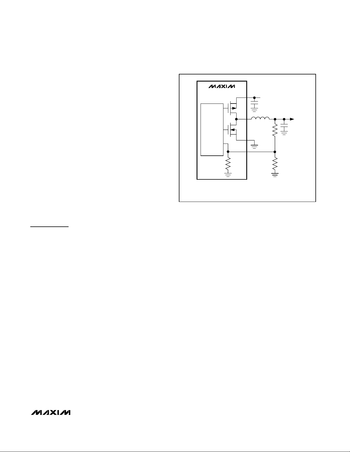
MAX8588
High-Efficiency, Low-I
Q
PMIC with
Dynamic Core for PDAs and Smartphones
______________________________________________________________________________________ 27
Note that the pole cancellation does not have to be
exact. RCx CCneed only be within 0.75 to 1.25 times
R
LOAD
x C
OUT
. This provides flexibility in component
selection.
If the output-filter capacitor has significant ESR, a zero
occurs at:
Z
ESR
= 1 / (2π x C
OUT
x R
ESR
)
If Z
ESR
> fC, it can be ignored, as is typically the case
with ceramic or polymer output capacitors. If Z
ESR
is
less than fC, it should be cancelled with a pole set by
capacitor CPconnected from CC_ to GND:
CP= C
OUTRESR
/ R
C
If CPis calculated to be < 10pF, it can be omitted.
Optimizing Transient Response
In applications that require load-transient response to
be optimized in favor of minimum component values,
increase the output-filter capacitor to increase the R in
the compensation RC. From the equations in the previous section, doubling the output cap allows a doubling
of the compensation R, which then doubles the transient gain.
Applications Information
Extending the Maximum Core
Voltage Range
The V3 output can be serially programmed to supply
from 0.7V to 1.475V in 25mV steps. In some cases, a
higher CPU core voltage may be desired. The V3 voltage range can be increased by adding two resistors as
shown in Figure 7.
R24 and R25 add a small amount of gain. They are set
so that an internally programmed value of 1.475V
results in a higher actual output at V3. The resistors
shown in Figure 1 set a maximum output of 1.55V, 1.6V,
or 1.65V. All output steps are shifted and the step size
is also slightly increased.
The output voltage for each programmed step of V3 in
Figure 7 is:
V3 = V3
PROG
+ (R24[(V3
PROG
/ R25) +
(V3
PROG
/ 185,500)])
where V3 is the actual output voltage, V3PROG is the
original programmed voltage from the “OUTPUT (V)”
column in Table 2, and 185,500 is the internal resistance of the FB3 pin.
Backup-Battery and V7 Configurations
The MAX8588 includes a backup-battery connection,
BKBT, and an output, V7. These can be utilized in different ways for various system configurations.
Primary Backup Battery
A connection with a primary (nonrechargeable) lithium
coin cell is shown in Figure 6. The lithium cell connects to
BKBT directly. V7 powers the CPU VCC_BATT from either
V1 (if enabled) or the backup battery. It is assumed
whenever the main battery is good, V1 is on (either with
its DC-DC converter or sleep LDO) to supply V7.
No Backup Battery (or Alternate Backup)
If no backup battery is used, or if an alternate backup
and VCC_BATT scheme is used that does not use the
MAX8588, then BKBT should be biased from IN with a
small silicon diode (1N4148 or similar, as in Figure 8).
BKBT must still be powered when no backup battery is
used because DBO, RSO, and POK require this supply
to function. If BKBT is not powered, these outputs do
not function and are high impedance.
Figure 7. Addition of R24 and R25 increases maximum core
voltage. The values shown raise the maximum core from
1.475V to 1.55V.
MAX8588
STEP-DOWN
PWM
REG3
**OTHER R24 VALUES:
R24 = 5.5kΩ, V3: 0.759V TO 1.60V
R24 = 7.7kΩ, V3: 0.783V TO 1.65V
PV3
PG3
185.5kΩ
LX3
FB3
TO BATT
R24**
3.3kΩ
R25
100kΩ
V3
VCC_CORE
1.55V MAX
Page 28

MAX8588
High-Efficiency, Low-IQPMIC with
Dynamic Core for PDAs and Smartphones
28 ______________________________________________________________________________________
Rechargeable Li+ Backup Battery
If more backup power is needed and a primary cell has
inadequate capacity, a rechargeable lithium cell can be
accommodated as shown in Figure 9. A series resistor
and diode charge the cell when the 3.3V V1 supply is
active. In addition to biasing V7, the rechargeable battery may be required to also power other supplies.
Rechargeable NiMH Backup Battery
In some systems, a NiMH battery may be desired for
backup. Usually this requires multiple cells because
the typical NiMH cell voltage is only 1.2V. By adding a
small DC-DC converter (MAX1724), the low-battery
voltage is boosted to 3V to bias BKBT (Figure 10). The
DC-DC converter’s low operating current (1.5µA typ)
allows it to remain on constantly so the 3V BKBT bias is
always present. A resistor and diode trickle charge the
NiMH cell when the main power is present.
PC Board Layout and Routing
Good PC board layout is important to achieve optimal
performance. Conductors carrying discontinuous currents and any high-current path should be made as
short and wide as possible. A separate low-noise
ground plane containing the reference and signal
grounds should connect to the power-ground plane at
only one point to minimize the effects of power-ground
currents. Typically, the ground planes are best joined
right at the IC.
Keep the voltage feedback network very close to the
IC, preferably within 0.2in (5mm) of the FB_ pin. Nodes
with high dV/dt (switching nodes) should be kept as
small as possible and should be routed away from
high-impedance nodes such as FB_.
Figure 8. BKBT connection when no backup battery is used, or
if an alternate backup scheme, not involving the MAX8588, is
used.
Figure 9. A 1-cell rechargeable Li+ battery provides more backup power when a primary cell is insufficient. The cell is charged
to 3.3V when V1 is active. Alternately, the battery can be
charged from IN if the voltages are appropriate for the cell type.
Figure 10. A 1-cell NiMH battery can provide backup by boosting with a low-power DC-DC converter. A series resistor-diode
trickle charges the battery when the main power is on.
MAIN
POWER
4.7µF
D1
1N4148
1µF
IN
MAX8588
BKBT
V7
MAIN
POWER
4.7µF
1kΩ
Li+ RECHARGEABLE
1-CELL
BACKUP BATTERY
4.7µF
1µF
10kΩ
1N4148
MURATA
LQH32C 10µH
1-CELL
NiMH
RECHARGEABLE
BACKUP BATTERY
4.7µF
BATT
MAX1724
EZK30
GND
SHDN
OUT
LX
10µF
IN
V1
BKBT
V7
MAIN
POWER
4.7µF
MAX8588
3.0V
1µF
IN
MAX8588
BKBT
V7
Page 29

MAX8588
High-Efficiency, Low-I
Q
PMIC with
Dynamic Core for PDAs and Smartphones
______________________________________________________________________________________ 29
Pin Configuration
Chip Information
TRANSISTOR COUNT: 13,958
PROCESS: BiCMOS
TOP VIEW
BKBT
SLPIN
LB1
CC1
FB1
FB2
CC2
POK
SCL
SLP
PV1
LX1
PG1
ON1
DBI
48
47 46 45
1
2
3
4
5
V7
6
V1
7
8
V2
9
10
11
12
13
14 15 16
PV2
LBO
SDA
PWM3
IN6V6ON6
44 43 42 414039 38
MAX8588ETM
17 18 19 202122 23
IN
LX2
PG2
RAMP
GND
THIN QFN
6mm × 6mm
FB3
REF
CC3
BYP
MR
37
36
RSO
35
SRAD
34
ON3
33
PV3
32
LX3
31
PG3
30
ON5
29
V5
28
IN45
27
V4
26
ON4
25
ON2
24
DBO
Page 30

MAX8588
High-Efficiency, Low-IQPMIC with
Dynamic Core for PDAs and Smartphones
30 ______________________________________________________________________________________
Package Information
(The package drawing(s) in this data sheet may not reflect the most current specifications. For the latest package outline information,
go to www.maxim-ic.com/packages
.)
D
D/2
e
A1 A2
E/2
E
A
(NE-1) X e
L
L1
k
D2
C
L
D2/2
(ND-1) X e
C
L
e e
b
e
E2/2
C
E2
L
k
L
C
L
LL
QFN THIN 6x6x0.8.EPS
PACKAGE OUTLINE
36, 40, 48L THIN QFN, 6x6x0.8mm
21-0141
1
E
2
Page 31

MAX8588
High-Efficiency, Low-I
Q
PMIC with
Dynamic Core for PDAs and Smartphones
Maxim cannot assume responsibility for use of any circuitry other than circuitry entirely embodied in a Maxim product. No circuit patent licenses are
implied. Maxim reserves the right to change the circuitry and specifications without notice at any time.
Maxim Integrated Products, 120 San Gabriel Drive, Sunnyvale, CA 94086 408-737-7600 ____________________ 31
© 2005 Maxim Integrated Products Printed USA is a registered trademark of Maxim Integrated Products, Inc.
Package Information (continued)
(The package drawing(s) in this data sheet may not reflect the most current specifications. For the latest package outline information,
go to www.maxim-ic.com/packages
.)
NOTES:
1. DIMENSIONING & TOLERANCING CONFORM TO ASME Y14.5M-1994.
2. ALL DIMENSIONS ARE IN MILLIMETERS. ANGLES ARE IN DEGREES.
3. N IS THE TOTAL NUMBER OF TERMINALS.
4. THE TERMINAL #1 IDENTIFIER AND TERMINAL NUMBERING CONVENTION SHALL CONFORM TO JESD 95-1
SPP-012. DETAILS OF TERMINAL #1 IDENTIFIER ARE OPTIONAL, BUT MUST BE LOCATED WITHIN THE
ZONE INDICATED. THE TERMINAL #1 IDENTIFIER MAY BE EITHER A MOLD OR MARKED FEATURE.
5. DIMENSION b APPLIES TO METALLIZED TERMINAL AND IS MEASURED BETWEEN 0.25 mm AND 0.30 mm
FROM TERMINAL TIP.
6. ND AND NE REFER TO THE NUMBER OF TERMINALS ON EACH D AND E SIDE RESPECTIVELY.
7. DEPOPULATION IS POSSIBLE IN A SYMMETRICAL FASHION.
8. COPLANARITY APPLIES TO THE EXPOSED HEAT SINK SLUG AS WELL AS THE TERMINALS.
9. DRAWING CONFORMS TO JEDEC MO220, EXCEPT FOR 0.4mm LEAD PITCH PACKAGE T4866-1.
10. WARPAGE SHALL NOT EXCEED 0.10 mm.
PACKAGE OUTLINE
36, 40, 48L THIN QFN, 6x6x0.8mm
21-0141
2
E
2
 Loading...