

Page 1
For free samples & the latest literature: http://www.maxim-ic.com, or phone 1-800-998-8800.
For small orders, phone 408-737-7600 ext. 3468.
_______________General Description
The MAX845 provides an isolated power supply small
enough to fit in thin PCMCIA cards and space-sensitive
applications. It drives a low-profile center-tapped transformer primary from a 5V or 3.3V DC power supply. The
secondary can be wound to provide any isolated positive or negative voltage at powers up to 750mW.
The MAX845 consists of an oscillator followed by a toggle flip-flop. The flip-flop generates two 50% duty-cycle
square waves, which are complementary at half the
oscillator frequency (450kHz, min). These two signals
drive the ground-referenced N-channel power switches. Internal circuitry ensures break-before-make action
between the two switches.
A low-power shutdown disables both the switches and
the oscillator, reducing power consumption. An evaluation kit (MAX845EVKIT-MM) is available to evaluate lowprofile 5V 40mA and 5V 100mA applications.
________________________Applications
PCMCIA Modem Cards
Isolated Data Acquisition
Isolated Interface Power Supply
Noise-Immunity Communications Interface
Bridging Ground Differences
Medical Equipment
Process Control
Low-Power LAN Networks
____________________________Features
♦ Transformer Driver for Ultra-Thin 5V-µs Transformers
♦ Isolated DC-to-DC Power Supply for PCMCIA
Applications
♦ 450kHz Minimum Switching Frequency
♦ Ultra-Low Input Supply Current Ripple
♦ Single +5V or +3.3V Supply
♦ 5µW Low-Power Shutdown Mode
♦ 8-Pin SO and µMAX Packages
♦ Low Output Ripple Permits Miniature Output
Capacitors
MAX845
Isolated Transformer Driver
for PCMCIA Applications
________________________________________________________________
Maxim Integrated Products
1
1
2
3
4
8
7
6
5
D2
GND2
V
CC
N.C.
SD
FS
GND1
D1
SO/µMAX
TOP VIEW
MAX845
___________________Pin Configuration
MAX845
D1
D2FS
GND1 GND2
V
CC
1
8
46
27
3
V
IN
SD
FREQUENCY
SELECT
C2
C1
C3
5V @ 150mA
OUTPUT
5V
ON / OFF
T1
CR2
CR1
__________Typical Operating Circuit
19-0372; Rev 4; 10/97
PART
MAX845C/D
MAX845EUA -40°C to +85°C
0°C to +70°C
TEMP. RANGE PIN-PACKAGE
Dice*
8 µMAX
EVALUATION KIT
AVAILABLE
*Contact factory for dice specifications.
_______________Ordering Information
MAX845ESA -40°C to +85°C 8 SO
Page 2
MAX845
Isolated Transformer Driver
for PCMCIA Applications
2 _______________________________________________________________________________________
ABSOLUTE MAXIMUM RATINGS
ELECTRICAL CHARACTERISTICS
(VCC= 5V ±10%, TA= T
MIN
to T
MAX
, unless otherwise noted. Typical values are at TA= +25°C.)
Stresses beyond those listed under “Absolute Maximum Ratings” may cause permanent damage to the device. These are stress ratings only, and functional
operation of the device at these or any other conditions beyond those indicated in the operational sections of the specifications is not implied. Exposure to
absolute maximum rating conditions for extended periods may affect device reliability.
Note 1: Operating supply current is the current used by the MAX845 only. Load current is not included.
Note 2: Shutdown supply current includes output switch leakage currents.
Supply Voltage (V
CC
)...............................................-0.3V to +7V
Control Input Voltage (SD, FS)...................-0.3V to (V
CC
+ 0.3V)
Peak Output Switch Current (D1, D2)......................................1A
Output Switch Voltage (D1, D2).............................................12V
Average Output Switch Current (D1, D2) .........................200mA
Continuous Power Dissipation (T
A
= +70°C)
SO (derate 5.88mW/°C above +70°C).........................471mW
µMAX (derate 4.10mW/°C above +70°C) ....................330mW
Operating Temperature Range ...........................-40°C to +85°C
Storage Temperature Range.............................-65°C to +160°C
Junction Temperature......................................................+150°C
Lead Temperature (soldering, 10sec).............................+300°C
FS = V
CC
= 5.5V
FS = VCC= 4.5V
D1, D2; 100mA
Low
FS = V
CC
FS = 0V
High
SD = V
CC
FS = 0V, VCC= 4.5V
FS = 0V, VCC= 5.5V
Low
No load, SD = 0V, FS = V
CC
High
CONDITIONS
V2.5 2.2
µA
10
FS Input Current
50
V
0.8
FS Input Threshold
2.4
550 860 1100
450 675 900
Ω1.5 4.0Switch On-Resistance
pA10Shutdown Input Leakage Current
V
0.8
Shutdown Input Threshold
2.4
µA0.4Shutdown Supply Current (Note 2)
500
kHz
575
Switch Frequency
mA1.1 5.0Operating Supply Current (Note 1)
UNITSMIN TYP MAXPARAMETER
Minimum Start-Up Voltage
Page 3
MAX845
Isolated Transformer Driver
for PCMCIA Applications
_______________________________________________________________________________________
3
40
-20 60
OUTPUT RESISTANCE vs. TEMPERATURE
30
MAX845-01
TEMPERATURE (°C)
OUTPUT RESISTANCE (Ω)
20 100
20
15
10
35
25
-40 0 8040
VIN = 4.5V
VIN = 5.5V
FIGURE 11c
7.5
2.5
-20 60
OUTPUT RESISTANCE vs. TEMPERATURE
3.5
6.0
MAX845-02
TEMPERATURE (°C)
OUTPUT RESISTANCE (Ω)
20 100
5.0
4.5
3.0
4.0
7.0
6.5
5.5
-40 0 8040
FIGURE 11b
1.6
1.4
1.2
0.2
-20 60
SHUTDOWN SUPPLY CURRENT
vs. TEMPERATURE
MAX845-03
TEMPERATURE (°C)
SHUTDOWN CURRENT (µA)
20 100
0.6
1.0
-40 0 8040
0.8
0.4
SD = V
CC
1000
950
600
-20 60
D1, D2 FREQUENCY vs. TEMPERATURE
MAX845-04
TEMPERATURE (°C)
FREQUENCY (kHz)
20 100
750
900
850
-40 0 8040
800
700
650
VIN = 5.5V
VIN = 4.5V
VIN = 5.0V
VIN = 6.0V
90
100
0
60
140 160
EFFICIENCY vs. LOAD CURRENT
20
70
MAX845-07
LOAD CURRENT (mA)
EFFICIENCY (%)
20 100
50
40
10
30
80
60
0
8040
120
FIGURE 11b
FIGURE 11c
850
800
500
550
-20 60
D1, D2 FREQUENCY vs. TEMPERATURE
MAX845-05
TEMPERATURE (°C)
FREQUENCY (kHz)
20 100
650
750
-40
0 8040
700
600
FS HIGH
VIN = 5.0V
FS LOW
1.5
1.4
0.8
-20 60
SUPPLY CURRENT vs. TEMPERATURE
MAX845-06
TEMPERATURE (°C)
SUPPLY CURRENT (mA)
20 100
1.0
-40 0 8040
0.9
1.1
1.3
1.2
1.7
1.6
VIN = 4.5V
VIN = 5.0V
VIN = 5.5V
VIN = 6.0V
7.5
2.5
0 40
OUTPUT VOLTAGE vs. LOAD CURRENT
3.5
6.5
MAX845-08
LOAD CURRENT (mA)
OUTPUT VOLTAGE (V)
80
5.5
4.5
3.0
4.0
7.0
6.0
5.0
20 60 140120100 160
TRANSFORMERS
USED IN FIGURE 11b
TGM-010P3
TGM-030P3
TGM-020P3
15
5
0 40
OUTPUT VOLTAGE vs. LOAD CURRENT
7
13
MAX845-09
LOAD CURRENT (mA)
OUTPUT VOLTAGE (V)
80
11
9
6
8
14
12
10
20 60 140120100 160
TRANSFORMERS
USED IN FIGURE 11c
TGM-010P3
TGM-030P3
TGM-020P3
__________________________________________Typical Operating Characteristics
(
Typical Operating Circuit
, VIN= 5V, C1 = 0.1µF, C2 = C3 = 0.33µF, T1 = Halo TGM-010P3, CR1 = CR2 = MBR0520, FS = VCC,
T
A
= +25°C, unless otherwise noted.)
Page 4
MAX845
Isolated Transformer Driver
for PCMCIA Applications
4 _______________________________________________________________________________________
____________________________Typical Operating Characteristics (continued)
(
Typical Operating Circuit
, VIN= 5V, C1 = 0.1µF, C2 = C3 = 0.33µF, T1 = Halo TGM-010P3, CR1 = CR2 = MBR0520, FS = VCC,
TA= +25°C, unless otherwise noted.)
SWITCHING WAVEFORMS
(TWO CYCLES)
5V/div
400ns/div
D1
D2
SWITCHING WAVEFORM
(BREAK-BEFORE-MAKE)
500mV/div
200ns/div
D2OFFD1OFF
CIRCUIT
OF FIG. 1
D2ON D1ON
TIME FROM SHUTDOWN TO POWER-UP
2V/div
5µs/div
SD
OUTPUT
_____________________Pin Description
No Connect. Not internally connected.N.C.5
+5V Supply VoltageV
CC
6
Ground. Connect both GND1 and GND2 to
ground.
GND27
Open Drain of N-Channel Transformer Drive 2D28
Shutdown. Ground for normal operation,
connect to V
CC
for shutdown.
SD4
Frequency Select (internal pull-up). If FS =
VCCor open, switch frequency = 725kHz; if
FS = 0V, switch frequency = 535kHz.
FS3
PIN
Ground. Connect both GND1 and GND2 to
ground.
GND12
Open Drain of N-Channel Transformer Drive 1D11
FUNCTIONNAME
Figure 1. Test Circuit
V
IN
5V
ON / OFF
FREQUENCY
SELECT
C1
0.1µF
4
SD
3
6
V
CC
MAX845
GND1 GND2
2 7
R1
50Ω
1
D1
R2
50Ω
8
D2FS
Page 5
_______________Detailed Description
The MAX845 is a transformer driver specifically
designed to provide isolated power for PCMCIA and
other height- and/or space-sensitive applications. It
drives a center-tapped transformer primary from a 5V
or 3.3V DC power supply. The secondary can be
wound to provide any isolated DC voltage needed at
power levels up to 750mW.
The 450kHz minimum switching frequency allows the
use of very thin transformers, making the MAX845 ideal
for PCMCIA and other space-limited applications. The
MAX845 is designed to drive a single transformer less
than 0.09 inches (2.3mm) in height, including package.
Further reduction down to 0.050 inches (1.27mm) can
be achieved using a transformer without a package.
The MAX845 consists of an RC oscillator driving a pair
of N-channel power switches. The oscillator runs at
double the output frequency, driving a toggle flip-flop
to ensure 50% duty cycle to each of the switches.
Internal circuitry ensures break-before-make action
between the two switches.
A low-current shutdown mode disables all internal circuitry, including the oscillator and both power switches.
Drive the shutdown pin (SD) high to shut down the part;
drive SD low for normal operation. The SD pin has no
internal default condition and must not be allowed to
float.
Most MAX845 applications will operate at high frequencies. The frequency-select pin (FS) is pulled high or left
open (FS is internally pulled up to VCC) to operate at a
minimum of 450kHz. Pulling FS low selects the low-frequency state.
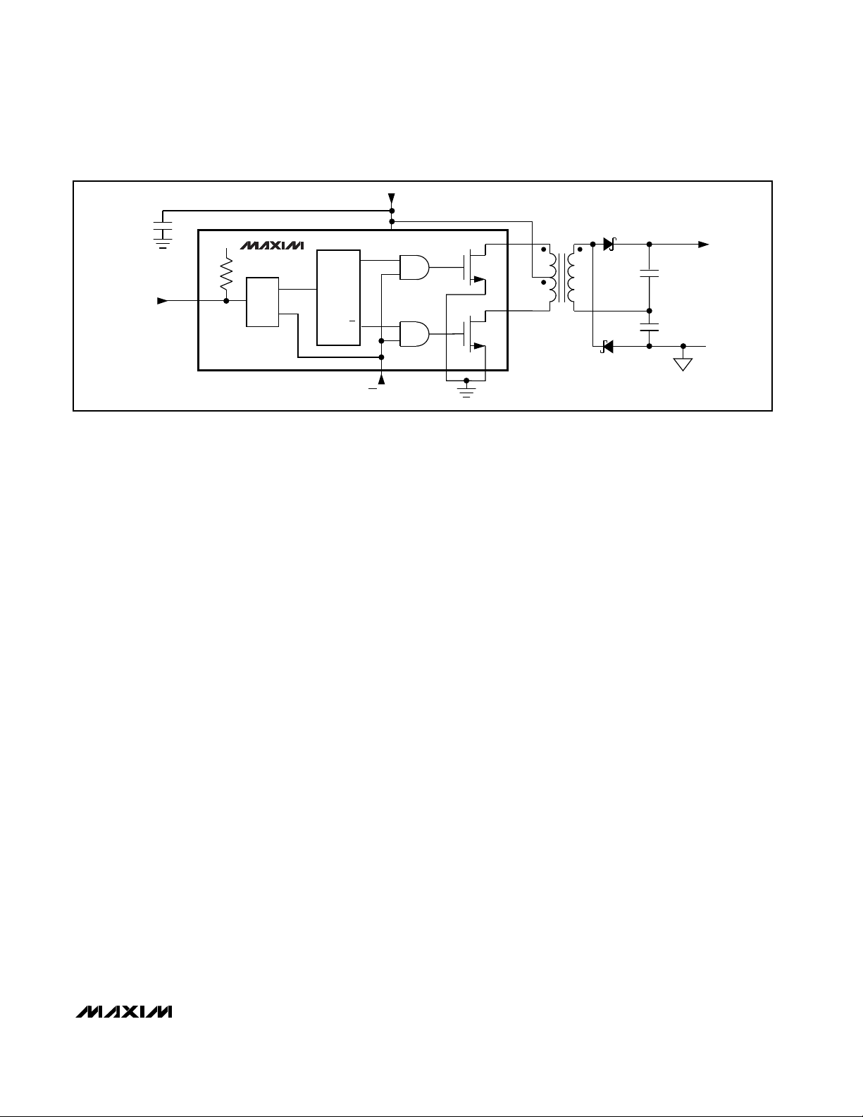
Theory of Operation
Figure 2 shows the MAX845 driving both a TGM-010P3
transformer with a center-tapped primary, and a secondary with a voltage-doubler rectifier topology. All of the
transformers driven by the MAX845 must have a center
tap with VINapplied. Whenever one of the MAX845 outputs (D1 or D2) goes low, the other goes to approximately double the supply voltage. A voltage is induced in the
secondary and the rectifier diodes steer the currents into
the appropriate output capacitor. On alternate half
cycles, each capacitor is charged. The output voltage is
the sum of the voltages from each output capacitor. This
topology yields the simplest and smallest transformer
because the least number of secondary turns is required
for a given voltage.
__________Applications Information
With the MAX845 transformer driver, designers have
the advantages of push/pull converter topology in
space-sensitive applications. The push/pull DC-DC
converter topology allows isolated multiple outputs,
step-up/step-down or inverted outputs, easier filtering
on the input and the output, and lower overall noise.
Isolated Power for PCMCIA Applications
Medical instrumentation, modems, and LAN-interface
cards often require isolated power supplies. One of the
best switching-regulator topologies for this application
is the push/pull forward-converting DC-DC power supply shown in Figures 3 and 4. Because the transformer
works in the forward mode (rather than the flyback
mode), its core does not store energy and, therefore,
can be small. Input and output capacitors can be small
because of the high-frequency and continuous-current
waveforms.
MAX845
Isolated Transformer Driver
for PCMCIA Applications
_______________________________________________________________________________________ 5
MAX845
D1
D2
FS
GND2 GND1
V
CC
FREQUENCY
SELECT
C2
C3
C1
OUTPUT
5V @ 150mA
5V
N
N
Q
Q
OSC
F / F
V
IN
SD
ON / OFF
400kHz/
700kHz
T
ISO
GND
V
CC
CR1
CR2
Figure 2. Detailed Block Diagram
Page 6

MAX845
The MAX845 is a versatile transformer driver, capable
of driving a center-tapped transformer primary from a
5V or 3.3V DC power supply (Figures 3 and 4). The
secondary can be wound to provide any isolated voltage needed at power levels up to 750mW with a 5V
supply or up to 500mW with a 3.3V supply. Figure 3
shows a typical 5V to isolated 5V application circuit that
delivers up to 150mA of isolated 5V power.
3.3V Supply
Any of the application circuits shown may be converted
to 3.3V operation by changing the turns ratio of the transformer and operating the MAX845 from a boost supply,
as shown in Figure 4. In normal operation, whenever one
of the MAX845 outputs goes low, the other goes to
approximately double the supply voltage. Since the circuit is symmetrical, the two outputs can be combined
with diodes, lightly filtered, then used to power the
MAX845, and possibly other light loads as well.
The diodes on the primary side may be any fast-switching small-signal diodes, such as the 1N914, 1N4148, or
CMPD2838. The value of the primary filter capacitor is
not critical and can be very small, since it only needs to
supply current to the MAX845 during the break-beforemake interval.
The transformer could be any of the same ones used for
5V operation, but for optimum performance it should
have fewer primary turns, as the ET product required is
now only 3.3V-µs. For a given power level, the currents
will be higher at 3.3V, so transformer winding resistance
will be more critical and efficiencies will be lower. The
MAX845 output current must still be limited to 200mA
(see
Absolute Maximum Ratings
), so the available out-
put power will be less than with a 5V power source.
Low-Noise Power Supply
The MAX845 topology is inherently low noise, in that
either one or the other of the two power devices is on at
any given time. By alternating between two identical
states with one side on and the other off, the input current is nearly constant and secondary output power is
available at all times. There is an intentional breakbefore-make action to prevent any possibility of both
power switches conducting at the same time. During
this 100ns non-overlap interval, the input current goes
to zero. This adds a small high-frequency component
to the input current waveform. This ripple current can
easily be absorbed by a small input bypass capacitor
(0.33µF) from VCCto ground. Figure 5 shows a lownoise bias supply using the MAX845 transformer driver.
When using the two-diode push-pull (Figure 11a)
rectifier or the four-diode bridge (Figure 11b), the output voltage tends to be more constant than in most
alternative topologies. As described above, the circuit
alternates between two identical states that both provide power to the load. The only part of the cycle that
produces output ripple is the 100ns non-overlap interval, which can easily be filtered by a small ceramic
output capacitor (0.33µF).
Isolated Transformer Driver
for PCMCIA Applications
6 _______________________________________________________________________________________
C2
0.33µF
C1
0.1µF
5V @ 150mA
ISO OUTPUT
5V
V
IN
MAX845
D1
D2FS
GND1 GND2
V
CC
1
8
6
2 7
3
FREQUENCY
SELECT
SD
4
ISO
GND
MBR0520
1CT:1.3CT
MBR0520
ON / OFF
Figure 3. 5V to Isolated 5V Application Circuit
MAX845
GND1 GND2
V
CC
1
8
6
2 7
1N4148
1N4148
D1
D2
3.3V
SUPPLY
SEE FIGURE 11
FOR RECTIFIER
CONFIGURATIONS
0.01µF
Figure 4. 3.3V Input to Isolated Output Application Circuit
Page 7

Isolated Data Conversion
Almost any serial-interface device is a candidate for
operation across an isolation barrier; Figure 6 illustrates
one example. The MAX176 analog-to-digital converter
(ADC) operates from +5V and -12V supplies, provided
by the multiple-tapped secondary and linear regulators.
This circuit easily supplies several hundred milliwatts of
additional isolated power for signal conditioning, multiplexing, or sensors. A +12V supply can be generated
by adding two more diodes from the ends of the secondary, and a -5V supply can be generated by connecting additional diodes to the 1⁄4and 3⁄4tap points on
the secondary. The MAX845 supplies sufficient power
for almost any Maxim ADC.
Telephone-Subscriber-Line Power Supply
The standard telephone system is placed in the “off
hook” state by placing a load on the line to signal the
central office that service is requested. Normally, most of
this power is wasted in a load resistor, but some systems
can benefit from utilizing this free power. Figure 7 shows
one way to transform the wasted telephone power to an
isolated, regulated 5V at currents up to 50mA.
Because the telephone line is a high-impedance
source, there can be a start-up problem with any DCto-DC converter; when the line voltage is low during
start-up, the frequency can be too low for the transformer, causing it to saturate. This excess saturation
current can keep the voltage from climbing to normal
operating levels. Thus the purpose of Q1, Q2, and the
associated resistors is to ensure that the MAX845
remains in the shutdown mode until the voltage is high
enough to allow proper operation.
Isolated 4mA to 20mA Analog Interface
The 4mA to 20mA current loop is widely used in the
process-control industry for transducer and actuator
control signals. These signals are commonly referred to
a distant ground that may be at a considerably higher
voltage with respect to the local ground. The circuit in
Figure 8 generates an isolated 4mA to 20mA current
from a 5V supply.
Isolated RS-485 Data Interface
The MAX845 power-supply transformer driver also provides isolated power for RS-485 data-interface applications. The application circuit of Figure 9 combines the
MAX845 with a low-dropout linear regulator, a transformer, several high-speed optocouplers, and a Maxim
RS-485 interface device.
Isolated RS-232 Data Interface
The MAX845 is ideal for isolated RS-232 data-interface
applications requiring more than four transceivers. Its
750mW output power capability enables it to drive 10
transceivers simultaneously. Figure 10 shows the typical application circuit for a complete 120kbps isolated
RS-232 data interface. This figure also shows how the
Sharp PC417 optocouplers can be replaced by the
lower-cost Quality Technologies 4N25 devices to
achieve data transfer rates up to 19.2kbps.
MAX845
Isolated Transformer Driver
for PCMCIA Applications
_______________________________________________________________________________________ 7
0.33µF
MAX845
D1
D2
FS
SD
GND1 GND2
N.C.
1
8
52 7
3
V
CC
6
4
MBR0520L*
5V
IN
*1N914 POSSIBLE FOR LOWER CURRENTS
0.33µF
IN OUT
GND
78L05
-5V
100mA
HALO
TGM-030P3
N.C.
Figure 5. Low-Noise Supply
Page 8

MAX845
Isolated Transformer Driver
for PCMCIA Applications
8 _______________________________________________________________________________________
10µF
6N136
MAX845
D1
FS
D2
GND1 GND2
V
CC
4
2 7
8
1
SD
6
3
6N136
6N136
10µF
79L12
78L05
1
2
3
4
8
7
6
5
1
2
3
4
8
7
6
5
1
2
3
4
8
7
6
5
1
2
3
4
8
7
6
5
CONVST
V
DD
V
SS
CLOCK
DATA
AIN
VREF
GND
MAX176
3k
3k
470Ω
0.1µF 10µF
0.1µF
10µF
0.1µF
10µF
200Ω
200Ω
8.2k
74HC04
7
6
5
4
3
2
1
15
16
QH
QG
QF
QE
QD
QC
QB
QA
SER
SCK
RCK
SCLR
14
11
12
10
74HC595
13 8
5V
INPUT
0.1µF
D11(MSB)
D10
D9
D8
5V
INPUT
7
6
5
4
3
2
1
15
16
QH
QG
QF
QE
QD
QC
QB
QA
SER
SCK
RCK
SCLR
14
11
12
10
74HC595
13 8
5V
INPUT
0.1µF
D7
D6
D5
D4
D3
D2
D1
D0 (LSB)
5V
INPUT
74HC04
ON/OFF
START
INPUT CLOCK
1CT : 1.5CT : 3CT
4 x 1N5817
V
IN
5V INPUT
SIGNAL
GROUND
ANALOG
INPUT
ISO
5V
ISO
-12V
8
QH
′
ISOLATION
BARRIER
Figure 6. Typical Isolated Data-Conversion Application
Page 9

MAX845
Isolated Transformer Driver
for PCMCIA Applications
_______________________________________________________________________________________ 9
0.1µF
ISO
GND
C1
0.1µF
5V @ 50mA
ISO OUTPUT
D1
TELEPHONE SUBSCRIBER LINE
2M
100k
1k
100k
100k
100k
680k
Q1
2N3906
Q2
2N3904
6.8V
2W
MAX845
D1
D2
FS
SD
GND1 GND2
V
CC
1
T1
1:2:1
8
3
22k
22k
N.C.
6
2 7
4
D2
1N5817
IC2
TL431
ISOLATION
BARRIER
D3
1N5817
IC1
Figure 7. 5V from Telephone-Subscriber Line
10µF
5V
MAX845
D1
D2
GND1 GND2
V
CC
1
8
6
2 7
1N5817
SD
4
1N5817
1CT:5CT
49.9k
7
6
3
2
4
7
6
3
2
4
10k
24.9Ω
2N3904
MAX480
MAX480
0.1V to 0.5V
ISO
5V
I
OUT
4mA to 20mA
78L05
4
3
2
1
5
6
24V UNREGULATED
49.9k
R
L
0k to 1k
2N3904
ISOLATION
BARRIER
V
IN
IN
GND
OUT
IL300
Figure 8. Typical 4mA/20mA Application Circuit
Page 10

MAX845
Isolated Transformer Driver
for PCMCIA Applications
10 ______________________________________________________________________________________
C3
0.1µF
C1
0.1µF
C2
2.2µF
ISO 5V
ISOLATION
BARRIER
5V
V
IN
MAX845
D1
D2
FS
GND1 GND2
V
CC
1
8
6
2 7
3
1N5817
SD
4
ON / OFF
390Ω
*74HC04
DE
RO
390Ω
*74HC04
DI
3.3k
1
3
5
4
6
1
2
4
3
5
4
1
3
6
*74HC04
*74HC04 OR EQUIVALENT
MAX883
56 4
SHDNSET GND
MAX481
MAX483
MAX485
MAX487
52
RE GND
C4
2.2µF
IN OUT
8 2
1N5817
390Ω
4
3.3k
3.3k
3
1
8
6
7
DI
DE
RO
A
B
PC410 / 417
PC357T
PC410 / 417
ICT:1.3CT
V
CC
485
I/O
N.C.
Figure 9. Typical RS-485 Application Circuit
Page 11

MAX845
Isolated Transformer Driver
for PCMCIA Applications
______________________________________________________________________________________ 11
C3
0.1µF
C2
2.2µF
ISO 5V
ISOLATION
BARRIER
5V
V
IN
1
8
5
C1
0.1µF
MBR0520
MAX845
D1
D2
GND1 GND2
V
CC
6
2 7
N.C.
SD
4
ON / OFF
10 x PC417
*74HC04 OR EQUIVALENT
MAX225
ENSD
C4
2.2µF
8 2
MBR0520
MAX883
56 4
SHDNSET GND
IN OUT
390Ω
3 11
13, 14
27, 28
T1
IN
T1
OUT
390Ω
*74HC04
T1
IN
1
2
4
5
6
1
24
5
6
390Ω
74HC04
T2
IN
390Ω
74HC04
T3
IN
390Ω
74HC04
T4
IN
390Ω
74HC04
T5
IN
74HC04
R1
OUT
74HC04
74HC04
74HC04
74HC04
R2
OUT
R3
OUT
R4
OUT
R5
OUT
5 x 3.3k
390Ω
390Ω
390Ω
390Ω
4 12
T2
IN
T2
OUT
25 18
T3
IN
T3
OUT
24 17
T4
IN
T4
OUT
23 16
T5
IN
T5
OUT
5 10
R1
OUT
R1
IN
6 9
R2
OUT
R2
IN
7 8
R3
OUT
R3
IN
22
19
R4
OUT
R4
IN
21
20
R5
OUT
R5
IN
V
CC
21
GND
5 x 3.3k
1N5711
6
5
4
1
2
390Ω
3.3k
V
CC
ISO
R
OUT
R
OUT
1CT:1.3CT
1N5711
1
2
6
5
4
390Ω
3.3k
V
CC
ISO
T
IN
T
IN
*74HC04
4N25 LOWER SPEED, LOWER COST ALTERNATE OPTOCOUPLER CONFIGURATIONS (FOR DATA RATES BELOW 9.6kbps)
FS
3
74HCO4
4N25
ISO
GND
4N25
ISO
GND
N.C.
Figure 10. Typical RS-232 Application Circuit
Page 12

______________Component Selection
Transformer
The MAX845 drives any transformer that has a centertapped primary and a saturation rating of at least 5V-µs
(ET product) per side. The oscillator frequency varies
linearly with VCC. The transformer is most vulnerable to
saturation at the minimum frequency, because the
switches are on for the longest period. At VCC= 4.5V,
the transformer must withstand at least:
1 1
4.5V x ———–——— x —= 5V-µs
450kHz min 2
And at VCC= 5.5V, the transformer must withstand
at least:
1 1
5.5V x ———–——— x — = 5V-µs
550kHz min 2
Thus, the required ET product is constant over the
entire 5V ±10% range.
Select either a toroid or a gapped core. Although some
applications will require custom transformers, many
can use standard transformer designs, such as those
listed in Table 1. Some of these manufacturers have
standard products designed for the MAX845, while
some have standard products that can be adapted for
specific customer requirements. Table 1 also lists some
suppliers of suitable magnetic cores.
An ungapped toroid core must never be allowed to saturate. An empirical way to measure a toroid’s ET product is to wind 20 turns on the bare core and observe
the current waveform on an oscilloscope while driving
the winding with a function generator. Generate a 50%
duty-cycle square wave at a test frequency of 500kHz,
with no DC offset. Gradually increase the driving voltage until the waveform suddenly begins to draw more
current. At this point, the core is saturating, so reduce
the driving voltage until the core just barely stops saturating. The ET product indicated is simply the maximum voltage that can be applied without saturation,
multiplied by 1µs (the time of half of the period of the
input signal). Because the ET product varies linearly
with the number of turns, this test winding can be
scaled up or down to act as a suitable primary for that
particular core.
A gapped core, such as a bobbin or drum core, is not
limited by ET product, but rather by inductance and
winding resistance. The primary inductance must be
high enough to prevent excessive current flow under
light-load conditions, yet low enough that it can be
wound on the core. Good results can be achieved by
using a primary inductance between 50µH and 200µH.
Calculate the number of turns required by using the
manufacturer’s A
L
(inductance per turn squared) value,
or measure a test winding with an inductance meter.
Inductance varies with the square of the number of turns.
While most MAX845 applications will use a toroid transformer for highest efficiency and lowest EMI, there may
be applications that can utilize less expensive transformers, such as E, I, or U-shaped cores, magnetic
bobbins, or etched windings on a printed circuit board.
Table 1 lists some transformer and core suppliers who
can assist with your magnetics design.
The secondary or secondaries can be scaled to produce
whatever output is required for the application at hand,
taking into account the rectifier topology to be used and
the forward voltage loss of the diodes selected.
Step-by-Step Transformer
Design Procedure
Before starting the design, determine the minimum and
maximum output voltage requirement, the minimum
and maximum load current, the physical size constraints, and the cost budget.
1) Select an appropriate core shape and material from
core vendors’ data sheets; trade-off EMI vs. space
and cost. Since the MAX845’s output waveform is a
square wave, it is rich in harmonics, so choose a
material with low losses at up to several MHz.
MAX845
Isolated Transformer Driver
for PCMCIA Applications
12 ______________________________________________________________________________________
Table 1. Transformer and Transformer-Core
Suppliers
TRANSFORMERS TRANSFORMER CORES
Halo Electronics
Phone: (415) 969-7313
FAX: (415) 367-7158
Ask for MAX845 Transformer
Magnetics Inc.
Phone: (412) 282-8282
FAX: (412) 282-6955
Coilcraft
Phone: (708) 639-6400
FAX: (708) 639-1469
Ask for MAX845 Transformer
Fair-Rite Products
Phone: (914) 895-2055
FAX: (914) 895-2629
BH Electronics
Phone: (612) 894-9590
FAX: (612) 894-9380
Ask for MAX845 Transformer
Philips Components
Phone: (401) 762-3800
FAX: (401) 762-3805, ext. 324
MMG (Magnetic Materials Group)
Phone: (201) 345-8900
FAX: (201) 345-1172
Amidon Associates
Phone: (714) 850-4660
FAX: (714) 850-1163
Sumida USA
Phone: (708) 956-0666
FAX: (708) 956-0702
Page 13

MAX845
Isolated Transformer Driver
for PCMCIA Applications
______________________________________________________________________________________ 13
2) Use a test winding to measure ET product (if using
an ungapped toroid) and/or ALvalue for the core.
3) Determine the number of turns required for the primary winding. For an ungapped toroid, ET product
from center-tap to D1 must be at least 5V-µs. Other
core types must have sufficient inductance to limit
D1 and D2 output current under minimum load conditions, and must not be allowed to saturate.
4) Select a rectifier topology based on performance
requirements (ripple vs. loss, and space required
for secondary winding). Refer to Table 2, Rectifier
Topology Trade-Offs.
5) Work backward from V
OUT
requirements to determine the secondary to primary turns ratio. Include
losses in the rectifier diodes, and estimate resistive
losses in the windings. For load currents exceeding 150mA, use a voltage step-down transformer to
step up the output current from the MAX845. Do
not exceed the MAX845’s absolute maximum output current rating (200mA).
6) Wind the transformer with the largest diameter wire
that will fit the winding area. Select a wire gauge to
fill the winding aperture as much as possible.
Larger diameter wire has lower resistance per unit
length. Doubling the wire diameter reduces resistive losses by a factor of four.
Bobbin or drum cores suffer from low coupling between
windings. This usually requires bifilar winding for the
two halves of the primary.
Due to the inherent complexity of magnetic circuit
design, it will be necessary to build a prototype and reiterate the design. If necessary, adjust the design by
altering the number of primary or secondary turns, or the
wire gauge. If using a different core material or geometry, evaluate its ET product or A
L
as described above.
Rectifier Topology
Figure 11 shows various rectifier topologies. Refer to
Table 2 for selection criteria. The turns ratio of the transformer must be set to provide the minimum required output voltage at the maximum anticipated load, with the
minimum expected input voltage. In addition, the calculations should allow for worst-case losses in the rectifiers. Since the turns ratio determined in this manner will
ordinarily produce a much higher voltage at the secondary under conditions of high input voltage and/or
light loading, be careful to prevent an overvoltage condition from occurring (see the Output Voltage vs. Load
Current graph in the
Typical Operating Characteristics
).
Diodes
Use fast-switching diode rectifiers. Ordinary silicon signal diodes like the 1N914 or 1N4148 may be used for
low output current levels (less than 50mA), but Schottky
diodes have a lower forward voltage drop and should
be used for higher-current applications. Central
Semiconductor has low-current Schottky diodes as
duals in SOT-23 packages (CMPSH-3 series). The
Nihon SB05W05C is a common-cathode dual in a SOT23; it works well in the two-diode full-wave configuration. The Motorola MBR0520 is an excellent choice for
all configurations.
Figure 11c. Voltage Doubler
Figure 11a. 2-Diode Push-Pull
Figure 11b. 4-Diode Bridge
V
IN
1
8
MAX845
GND1 GND2
V
CC
6
2 7
D1
D2
V
IN
6
V
CC
1
D1
MAX845
GND1 GND2
2 7
8
D2
V
IN
6
V
CC
D1
1
MAX845
GND1 GND2
2 7
8
D2
Page 14

Output Regulator
Since the output voltage is not regulated against
changes in the input voltage or load current, an output
voltage regulator may be needed. A series linear regulator gives good performance and reasonably good
efficiency at low cost. A shunt regulator costs less,
occupies less space, and gives adequate performance
for some applications.
Series regulators such as the MAX666, MAX667,
MAX882/MAX883/MAX884, or MAX603/MAX604 simplify designs. Just select one with the desired output voltage and current capability, and connect it.
The simplest voltage regulator is the shunt zener shown
in Figure 12. The series resistor (R
S
) value should be as
high as possible to still deliver the maximum expected
load current with minimum input voltage. Be sure that no
ratings are exceeded at maximum input voltage and
minimum load current conditions; under such conditions,
the zener diode may have to dissipate much more power
than the load. Alternatively, start with the maximum allowable zener dissipation and select the series resistor
under light-load, high-line conditions. Then verify that
there is sufficient output current available with worstcase low input voltage.
For better regulation than the simple shunt zener, consider a shunt regulator IC such as the TL431. This
device behaves like a zener diode whose voltage can
be programmed by a resistor ratio. It can be used as a
stand-alone device or can be boosted above its 150mA
maximum rating without compromising its accuracy by
adding a discrete PNP transistor, as shown in Figure 12.
The input power of a shunt regulator is nearly independent of load, so efficiency at light loads tends to be
worse than it would be with a series regulator.
Output Filter Capacitor
Ceramic capacitors can be used as output capacitors
because of the lower level of output ripple current. In
applications where output ripple is not critical, a 0.33µF
chip or ceramic capacitor is normally sufficient. Refer to
Table 3 for suggested capacitor suppliers.
In applications sensitive to output-ripple noise, the output filter capacitor (C2) should have a low equivalent
series resistance (ESR) and a low equivalent series
inductance (ESL), and its capacitance should remain
fairly constant over temperature.
Sprague 595D surface-mount solid tantalum capacitors
and Sanyo OS-CON through-hole capacitors are recommended, if space allows, due to their extremely low ESR.
Capacitor ESR usually rises at low temperatures, but OSCON capacitors provide very low ESR below 0°C.
Input Bypass Capacitor
The input bypass capacitor (C1) is not critical. Unlike
switching regulators, the MAX845’s supply current is
fairly constant, and is therefore less dependent on the
input bypass capacitor. A low-cost 0.33µF chip or
ceramic capacitor is normally sufficient for input
bypassing.
MAX845
Isolated Transformer Driver
for PCMCIA Applications
14 ______________________________________________________________________________________
R
S
SIMPLE SHUNT ZENER
R
S
TL431
22k
22k
PROGRAMMABLE-IC SHUNT REGULATOR (STAND ALONE)
PROGRAMMABLE-IC SHUNT REGULATOR WITH DISCRETE PNP
R
S
TL431
22k
22k
1k
2N2907
5V OUTPUT
5V OUTPUT
Figure 12. Shunt-Regulator Circuits
Page 15

MAX845
Isolated Transformer Driver
for PCMCIA Applications
______________________________________________________________________________________ 15
Table 2. Rectifier Topology Trade-Offs
TOPOLOGY ADVANTAGE DISADVANTAGE
2-Diode
Push/Pull
(Figure 11a)
• Only 3 external
components
• Low output ripple
• Single diode drop
• More turns on
transformer
4-Diode
Bridge
(Figure 11b)
• Simpler transformer
winding requirements
• Low output ripple
• 5 external
components
• Higher cost
• 2 diode drops
Voltage
Doubler
(Figure 11c)
• Fewest turns on
transformer
• 4 external
components
• Higher output
ripple
• 2 diode drops
___________________Chip Topography
V
CC
GND2
FS
0.085"
(2.159mm)
0.058"
(1.4732mm)
SD
D1 D2
GND1
SUPPLIERCAPACITOR
Low-ESR 267 Series
Matsuo
USA Phone: (714) 969-2491
FAX: (714) 960-6492
Ceramic
Murata Erie
USA Phone: (800) 831-9172
FAX: (404) 436-3030
Very Low-ESR 595D/293D
Series
Sprague Electric Co.
USA Phone: (603) 224-1961
FAX: (603) 224-1430
Table 3. Suggested Capacitor Suppliers
SUBSTRATE CONNECTED TO V
CC
TRANSISTOR COUNT: 31
Page 16

MAX845
Isolated Transformer Driver
for PCMCIA Applications
16 ______________________________________________________________________________________
________________________________________________________Package Information
8LUMAXD.EPS
SOICN.EPS
 Loading...