

Page 1
MAX828 MAX829
Switched Capacitor
V oltage Converters
The MAX828/829 are CMOS “charge–pump” voltage converters in
ultra–small SOT–23 5 lead packages. They invert and/or double an
input voltage which can range from +1.5V to +5.5V. Conversion
efficiency is typically >95%. Switching frequency is 12kHz for the
MAX828 and 35kHz for the MAX829.
External component requirement is only two capacitors (3.3µF
nominal) for standard voltage inverter applications. With a few
additional components a positive doubler can also be built. All other
circuitry, including control, oscillator , power MOSFETs are integrated
on–chip. Supply current is 50 µA (MAX828) and 115 µA (MAX829).
The MAX828 and MAX829 are available in a SOT–23 5 lead
surface mount package.
Features
• Charge Pump in SOT–23 5 Lead Package
• >95% Voltage Conversion Efficiency
• Voltage Inversion and/or Doubling
• Low 50 µA (MAX828) Quiescent Current
• Operates from +1.5V to +5.5V
• Up to 25 mA Output Current
• Only Two External Capacitors Required
• Tested Operating Temperature Range: –40°C to +85°C
http://onsemi.com
SOT–23–5
SN SUFFIX
PRELIMINARY INFORMATION
OUT
CASE TBD
PIN CONFIGURATION
(Top View)
1
2
V
in
–
3
C
5
4
+
C
GND
Typical Applications
• LCD Panel Bias
• Cellular Phones
• Pagers
• PDAs, Portable Dataloggers
• Battery–Powered Devices
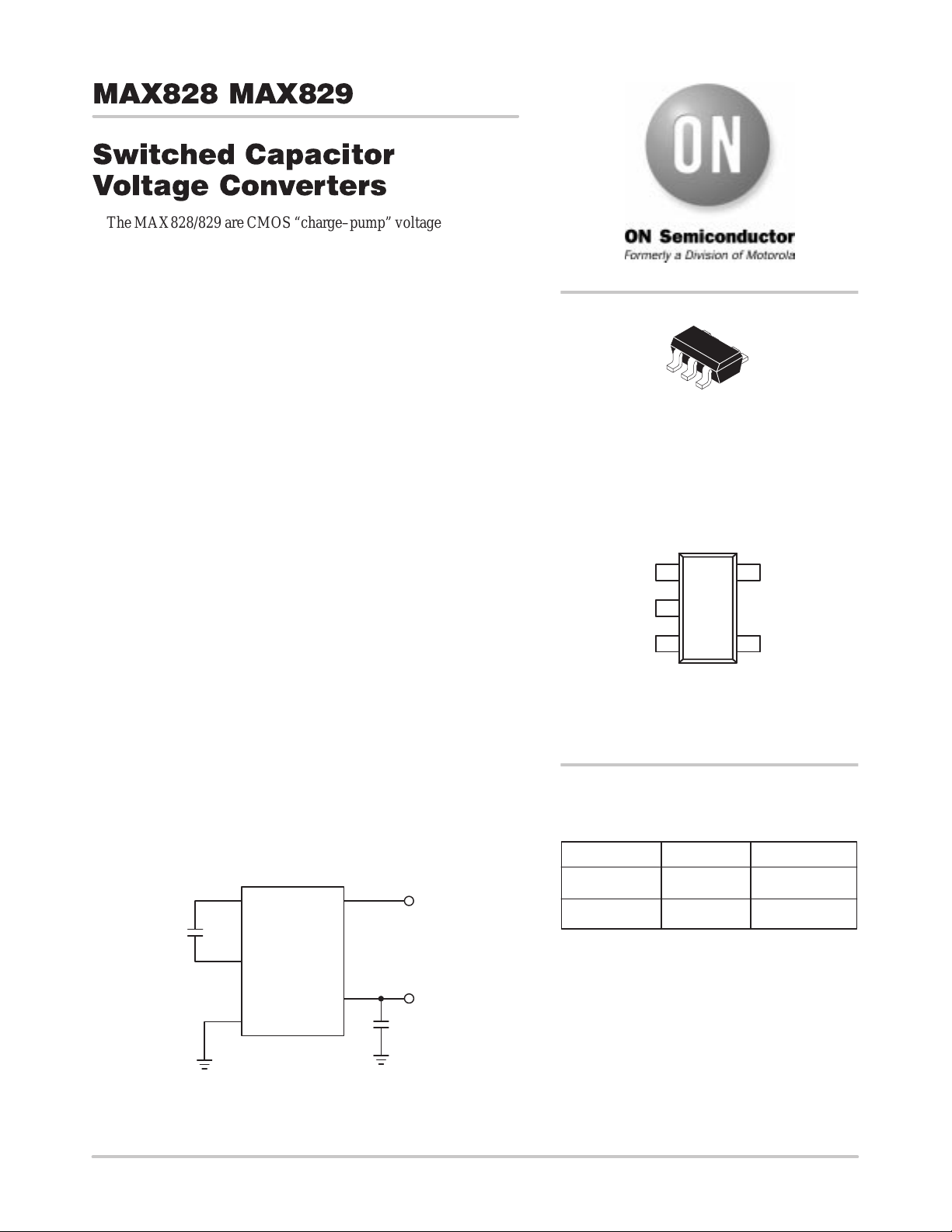
TYPICAL OPERATING CIRCUIT
Voltage Inverter
+
C
+
C1
–
C
GND
V
MAX828
MAX829
OUT
SOT–23–5*
NOTE: *SOT–23–5 is equivalent to EIAJ–SC74A
ORDERING INFORMATION
Device Package Shipping
MAX828SNTR SOT–23–5 3000 Tape/Reel
C2
INPUT
–
V
OUTPUT
MAX829SNTR SOT–23–5 3000 Tape/Reel
in
+
Semiconductor Components Industries, LLC, 1999
February , 2000 – Rev. 0
1 Publication Order Number:
MAX828/D
Page 2
MAX828 MAX829
ББББББ
ББББББ
ББББББ
ББББББ
ББББББ
PIN DESCRIPTION
Pin No. Symbol Description
1
2
3
4
4
ABSOLUTE MAXIMUM RATINGS*
Symbol Parameter Value Unit
T
A
P
D
T
stg
T
sol
* Maximum Ratings are those values beyond which damage to the device may occur.
OUT
V
IN
–
C
GND
+
C
Inverting charge pump output
Positive power supply input
Commutation capacitor negative terminal
Ground
Commutation capacitor positive terminal
Input Voltage (VIN to GND) +6.0, – 0.3 V
Output Voltage (OUT to GND) –6.0, +0.3 V
Current at OUT Pin 50 mA
Short–Circuit Duration – OUT to GND Indefinite
Operating Temperature Range –40 to +85 °C
Power Dissipation (TA ≤ 70°C) SOT–23–5
240 mW
Derate by 4mW/°C for TA > 70°C
Storage Temperature Range –65 to +150 °C
Lead Temperature (Soldering, 10 Seconds) +300 °C
ELECTRICAL CHARACTERISTICS (TA = 0°C to +85°C, V
otherwise noted
. Typical values are at TA = 25°C.)
= +5V , C1 = C2 = 10 µF (MAX828), C1 = C2 = 3.3µF (MAX829), unless
IN
Symbol Characteristic Min Typ Max Unit
I
V
F
P
V
R
DD
+
OSC
EFF
EFF
OUT
Supply Current (TA = 25°C)
MAX828
MAX829
Supply Voltage Range (R
LOAD
Oscillator Frequency (TA = 25°C)
MAX828
MAX829
Power Efficiency
I
= 3mA, TA = 25°C
LOAD
Voltage Conversion Efficiency (R
Output Resistance (Note 1.)
I
= 5mA, TA = 25°C
OUT
TA = 0°C to +85°C
= 10k
W)
—
—
— — 5.5 V
8.4
24.5
50
115
12
35
— 96 —
= R) 95 99.9 %
LOAD
—
—
25
—
90
µA
260
kHz
15.6
45.5
%
W
50
65
1. Capacitors C1 and C2 contribution is approximately 20% of the output impedance. For additional information, refer to Equation 1 in the
Applications Information section.
ELECTRICAL CHARACTERISTICS (TA = –40°C to +85°C, V
unless otherwise noted
Symbol
I
V
F
R
DD
in
OSC
OUT
Supply Current
Supply Voltage Range (R
Oscillator Frequency
Output Resistance (I
. Typical values are at TA = 25°C.) (Note 2.)
Characteristic Min Typ Max Unit
MAX828
MAX829
= 10k
W)
MAX828
MAX829
LOAD
= 5mA) — — 65
OUT
= +5V, C1 = C2 = 10µF (MAX828), C1 = C2 = 3.3µF (MAX829),
IN
—
—
—
—
115
325
1.5 — 5.5 V
6.0
19
—
—
20
54.3
µA
kHz
W
2. All –40°C to +85°C specifications are guaranteed by design.
http://onsemi.com
2
Page 3
MAX828 MAX829
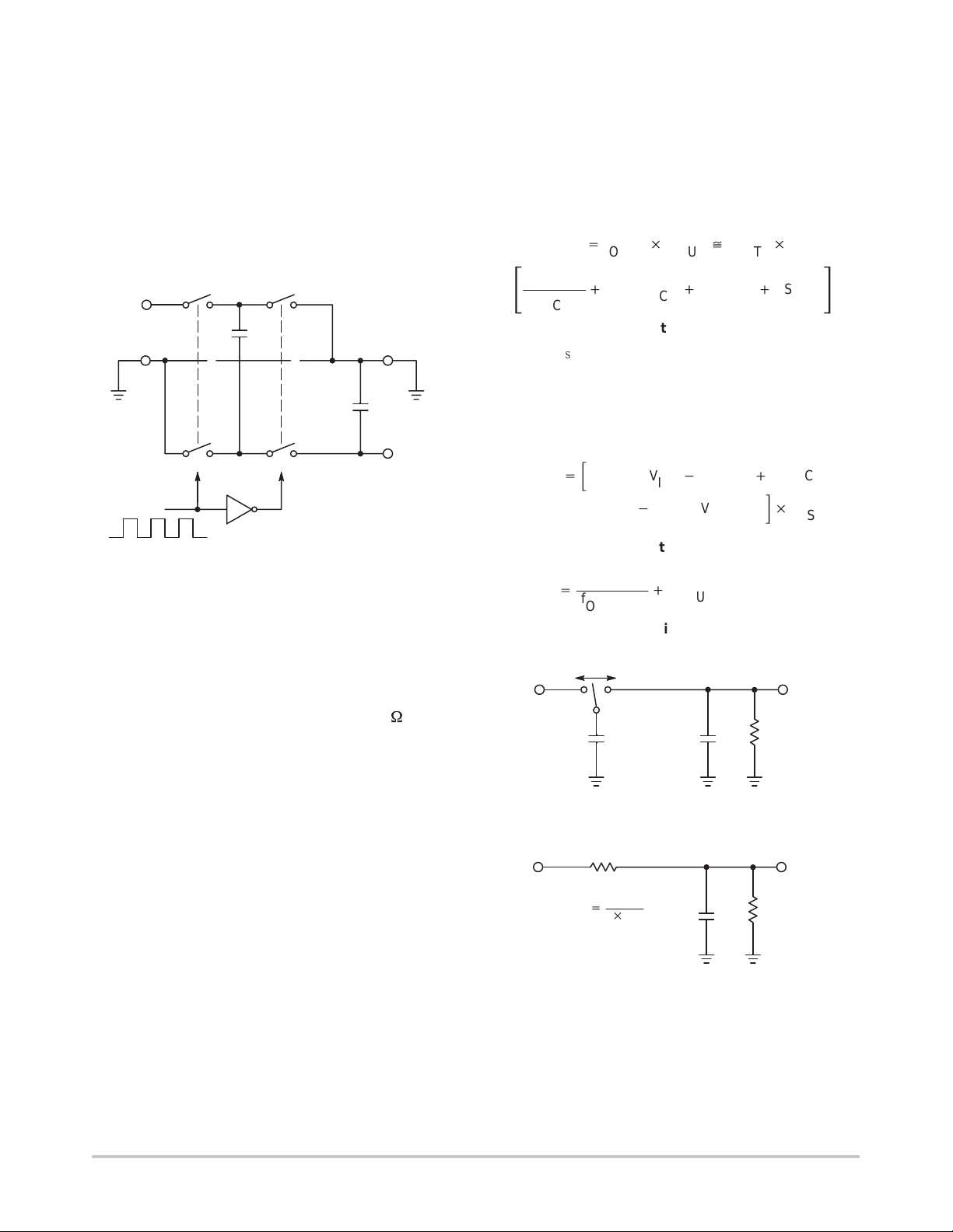
DET AILED OPERATING DESCRIPTION
The MAX828/829 charge pump converters invert the
voltage applied to the V
pin. Conversion consists of a
IN
two–phase operation (Figure 1). During the first phase,
switches S2 and S4 are open and S1 and S3 are closed.
During this time, C1 charges to the voltage on VIN and load
current is supplied from C2. During the second phase, S2
and S4 are closed, and S1 and S3 are open. This action
connects C1 across C2, restoring charge to C2.
IN
Figure 1. Ideal Switched Capacitor Charge Pump
S1 S2
C1
S3 S4
MAX828/829
C2
V
out
= –(Vin)
APPLICATIONS INFORMATION
Output Voltage Considerations
The MAX828/829 perform voltage conversion but do not
provide regulation. The output voltage will drop in a linear
manner with respect to load current. The value of this
equivalent output resistance is approximately 25W nominal
at +25°C and VIN = +5V . V
is approximately - 5V at light
OUT
loads, and droops according to the equation below:
(4) Losses that occur during charge transfer (from the
commutation capacitor to the output capacitor)
when a voltage difference between the two
capacitors exists.
Most of the conversion losses are due to factors (2), (3)
and (4) above. These losses are given by Equation 1.
P
LOSS(2,3,4)
1
ƪ
(f
OSC
The 1/(f
+
)
)C1
)(C1) term in Equation 1 is the effective output
OSC
2
I
OUT
8R
SWITCH
Equation 1.
R
OUT
)
^
4ESRC1)
I
OUT
2
ESR
C2
ƫ
resistance of an ideal switched capacitor circuit (Figures 2a,
2b).
The losses in the circuit due to factor (4) above are also
shown in Equation 2. The output voltage ripple is given by
Equation 3.
P
LOSS(4)
V
RIPPLE
+
V
+ƪ(0.5)(C1)(V
I
OUT
OSC
f
2
Equation 2.
)(C2)
Equation 3.
ƪ
(V
+
RIPPLE
(f
*
)
IN
2V
2
*
OUT
2(I
OUT
V
OUT
V
RIPPLE
)(ESRC2)
C2C1
2
))(0.5)(C2)
)ƫ
f
OSC
V
out
R
L
V
V
Charge Pump Efficiency
= I
DROP
= – (VIN – V
OUT
OUT
x R
OUT
DROP
)
The overall power efficiency of the charge pump is
affected by four factors:
(1) Losses from power consumed by the internal
oscillator, switch drive, etc. (which vary with input
voltage, temperature and oscillator frequency).
2
(2) I
R losses due to the on–resistance of the MOSFET
switches on–board the charge pump.
(3) Charge pump capacitor losses due to effective
series resistance (ESR).
http://onsemi.com
Figure 2a. Ideal Switched Capacitor Model
R
EQUIV
EQUIV
+
f C1
V
out
1
C2
R
L
+
V
R
Figure 2b. Equivalent Output Resistance
3
Page 4
MAX828 MAX829
Capacitor Selection
In order to maintain the lowest output resistance and
output ripple voltage, it is recommended that low ESR
capacitors be used. Additionally, larger values of C1 will
lower the output resistance and larger values of C2 will
reduce output ripple. (See Equation 3).
T able 1 shows various values of C1 and the corresponding
output resistance values at +25°C. It assumes a 0.1W ESR
and 0.5W RSW. Table 2 shows the output voltage ripple for
various values of C2. The V
output load current and 0.1W ESR
T able 1. Output Resistance vs. C1 (ESR = 0.1 Ω)
C1(µF)
0.1 1.7k 580
3.3 55 21
100 6.2 5.1
Table 2. Output Voltage Ripple vs. C2 (ESR = 0.1W) I
= 10mA
C2(µF) MAX828 V
3.3 250 87
100 8.3 2.9
MAX828 R
(W) MAX829 R
OUT
1 170 61
10 21 10
47 8.0 5.7
(mV) MAX829 V
RIPPLE
1 830 290
10 83 28
47 17 6.1
values assume 10mA
RIPPLE
.
C2
OUT
RIPPLE
(W)
OUT
(mV)
V
+
C3
3.3 mF*
+
OUT
15
C1
IN
2
–
C1
3
Voltage Inverter
C1
MAX828
MAX829
GND
C2
3.3 mF*
+
C1
3.3 mF*
4
*10 mF (MAX828)
in
V
out
+
R
L
Figure 3. T est Circuit
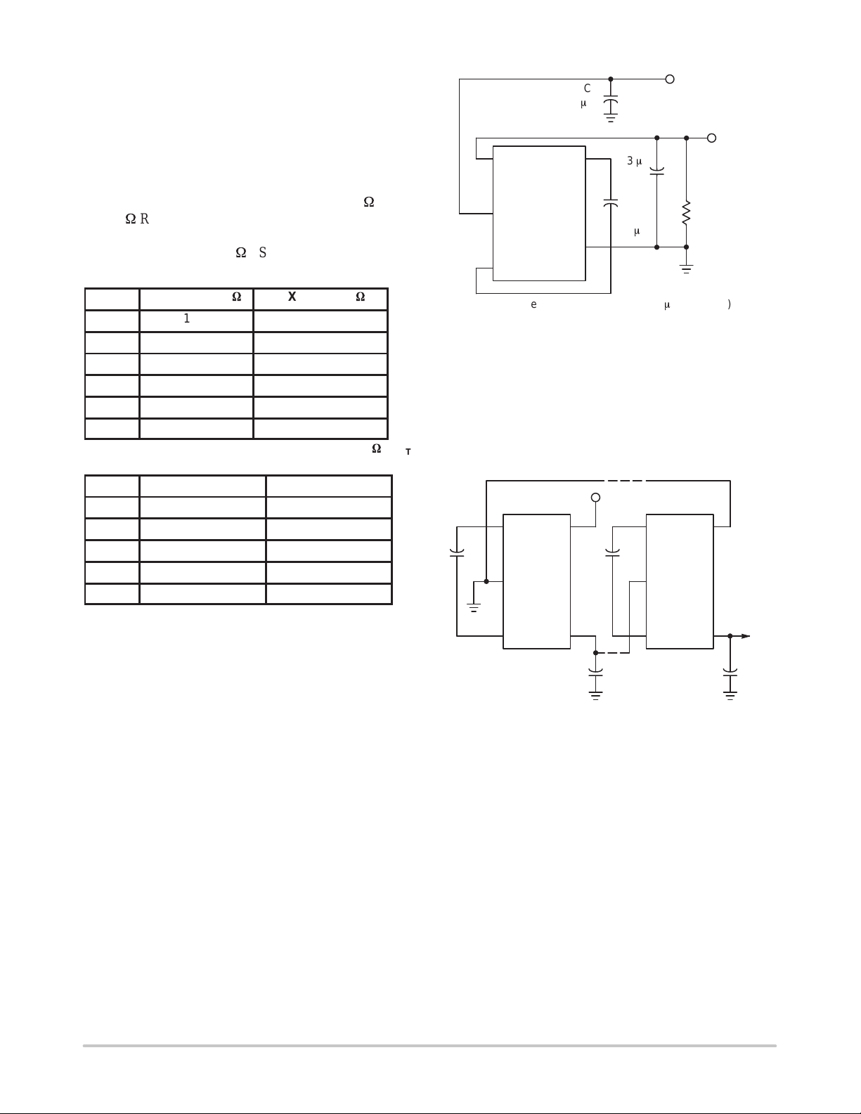
Cascading Devices
T wo or more MAX828/829’ s can be cascaded to increase
output voltage (Figure 4). If the output is lightly loaded, it
will be close to (- 2 x V
) but will droop at least by R
IN
OUT
of
the first device multiplied by the IQ of the second. It can be
seen that the output resistance rises rapidly for multiple
cascaded devices.
+
V
in
32
C1
+
4
MAX828
MAX829
“1”
32
C1
+
MAX828
MAX829
4
“n”
Input Supply Bypassing
The VIN input should be capacitively bypassed to reduce
AC impedance and minimize noise effects due to the
switching internal to the device. The recommended
capacitor depends on the configuration of the MAX828/829.
If the device is loaded from OUT to GND it is
recommended that a large value capacitor (at least equal to
C1) be connected from the input to GND. If the device is
loaded from IN to OUT a small (0.1µF) capacitor from IN
to OUT is sufficient.
V oltage Inverter
The most common application for charge pump devices is
the inverter (Figure 3). This application uses two external
capacitors - C1 and C2 (plus a power supply bypass
capacitor, if necessary). The output is equal to –V
plus any
IN
voltage drops due to loading. Refer to Table 1 and Table 2
for capacitor selection.
V
out
5
1
C2
5
+
V
= –nV
out
1
C2
+
in
Figure 4. Cascading MAX828s or MAX829s to
Increase Output V oltage
Paralleling Devices
T o reduce the value of R
, multiple MAX828/829s can
OUT
be connected in parallel (Figure 5). The output resistance
will be reduced by a factor of N where N is the number of
MAX828/829’s. Each device will require it’s own pump
capacitor (C1), but all devices may share one reservoir
capacitor (C2). However, to preserve ripple performance the
value of C2 should be scaled according to the number of
paralleled MAX828/829’s.
http://onsemi.com
4
Page 5

MAX828 MAX829
R
OF SINGLE DEVICE
R
32
C1
+
MAX828
MAX829
4
“1”
5
out
+
out
NUMBER OF DEVICES
+
V
in
C1
+
1
V
out
32
MAX828
MAX829
4
“n”
5
= V
...
–
in
C2
V
out
1
+
Figure 5. Paralleling MAX828s or MAX829s to
Reduce Output Resistance
V oltage Doubler/Inverter
Another common application of the MAX828/829 is
shown in Figure 6. This circuit performs two functions in
combination. C1 and C2 form the standard inverter circuit
described above. C3 and C4 plus the two diodes form the
voltage doubler circuit. C1 and C3 are the pump capacitors
and C2 and C4 are the reservoir capacitors. Because both
sub–circuits rely on the same switches if either output is
loaded, both will droop toward GND. Make sure that the
total current drawn from both the outputs does not total more
than 40mA.
Diode Protection for Heavy Loads
When heavy loads require the OUT pin to sink large
currents being delivered by a positive source, diode
protection may be needed. The OUT pin should not be
allowed to be pulled above ground. This is accomplished by
connecting a Schottky diode (1N5817) as shown in Figure
7.
GND
4
MAX828
MAX829
OUT
1
Figure 7. High V– Load Current
Layout Considerations
As with any switching power supply circuit good layout
practice is recommended. Mount components as close
together as possible to minimize stray inductance and
capacitance. Also use a large ground plane to minimize
noise leakage into other circuitry .
+
V
in
32
C1
+
MAX828
MAX829
4
5
C3
1
+
D1, D2 = 1N4148
D1
C2
+
D2
+
C4
V
out
V
out
(V
FD1
= V
= (2Vin) –
Figure 6. Combined Doubler and Inverter
in
) – (V
–
FD2
)
http://onsemi.com
5
Page 6

70
MAX828 MAX829
TYPICAL CHARACTERISTICS
Circuit of Figure 3, Vin = +5 V, C1 = C2 = C3, TA = +25°C, unless otherwise noted.
80
60
W
50
40
30
20
OUTPUT RESISTANCE ( )
10
0
40
35
30
25
20
15
MAX829
MAX828
SUPPLY VOLTAGE (V) TEMPERATURE (°C)
Figure 8. Output Resistance versus
Supply V oltage
Vin = 4.75 V, V
Vin = 3.15 V, V
= –4.0 V
out
out
= –2.5 V
70
W
60
50
40
30
20
OUTPUT RESISTANCE ( )
10
5.04.54.03.53.02.52.01.5
0
Vin = 1.5 V
Vin = 3.3 V
Vin = 5.0 V
85250–40
Figure 9. Output Resistance versus
T emperature
40
35
30
25
20
15
Vin = 4.75 V, V
Vin = 3.15 V, V
out
out
= –4.0 V
= –2.5 V
10
OUTPUT CURRENT (mA)
5
0
Figure 10. Output Current versus
450
)
p–p
400
350
300
250
200
150
100
OUTPUT VOLTAGE RIPPLE (mV
Vin = 4.75 V, V
50
0
Figure 12. Output V oltage Ripple versus
10
Vin = 1.9 V, V
CAPACITANCE (mF) CAPACITANCE (mF)
= –1.5 V
out
35302520151050
OUTPUT CURRENT (mA)
5
Vin = 1.9 V, V
0
Figure 11. Output Current versus
Capacitance (MAX828)
300
OUTPUT VOLTAGE RIPPLE (mV )
p–p
250
200
150
100
Vin = 4.75 V, V
50
0
= –4.0 V
out
Vin = 3.15 V, V
Vin = 1.9 V, V
CAPACITANCE (mF) CAPACITANCE (mF)
= –2.5 V
out
= –1.5 V
out
35302520151050
Capacitance (MAX829)
= –4.0 V
out
Vin = 3.15 V, V
out
Vin = 1.9 V, V
Figure 13. Output V oltage Ripple versus
Capacitance (MAX828)
Capacitance (MAX829)
= –2.5 V
= –1.5 V
out
= –1.5 V
out
35302520151050
35302520151050
http://onsemi.com
6
Page 7

MAX828 MAX829
TYPICAL CHARACTERISTICS
Circuit of Figure 3, Vin = +5 V, C1 = C2 = C3, TA = +25°C, unless otherwise noted.
120
100
m
80
60
40
SUPPLY CURRENT ( A)
20
MAX829
MAX828
PUMP FREQUENCY (kHz)
14
12
10
Vin = 5.0 V
Vin = 3.3 V
8
6
4
2
Vin = 1.5 V
PUMP FREQUENCY (kHz)
45
40
35
30
25
20
15
10
0
SUPPLY VOLTAGE (V) TEMPERATURE (°C)
Figure 14. Supply Current versus
Supply V oltage
5
0
TEMPERATURE (°C) OUTPUT CURRENT (mA)
Figure 16. Pump Frequency versus
T emperature (MAX829)
100
Vin = 5.0 V
Vin = 3.3 V
Vin = 1.5 V
5.04.54.03.53.02.52.01.5
0
85250–40
Figure 15. Pump Frequency versus
T emperature (MAX828)
0
–1
Vin = 2.0 V
–2
–3
–4
OUTPUT VOLTAGE (V)
–5
–6
85250–40
Vin = 3.3 V
Vin = 5.0 V
5030 4020100
Figure 17. Output Voltage versus
Output Current
EFFICIENCY (%)
Vin = 5.0 V
80
Vin = 3.3 V
Vin = 1.5 V
60
40
5030 4020100
OUTPUT CURRENT (mA)
Figure 18. Efficiency versus Output
Current
http://onsemi.com
7
Page 8

TAPING FORM
MAX828 MAX829
Component Taping Orientation for 5L SOT–23 Devices
USER DIRECTION OF FEED
DEVICE
MARKING
Tape & Reel Specifications Table
Package Tape Width (W) Pitch (P) Part Per Full Reel Diameter
5L SOT–23
MARKING
SOT–23–5
1234
MAX828/829 Marking
MAX828SNTR CA
MAX829SNTR CB
PIN 1
Standard Reel Component Orientation
for TR Suffix Device
(Mark Right Side Up)
8 mm 4 mm 3000 7 inches
+
1 2
+ Date Code
3 4
http://onsemi.com
8
Page 9

P ACKAGE DIMENSIONS
0.75 (1.90)
REFERENCE
MAX828 MAX829
SOT–23–5
PLASTIC PACKAGE
CASE TBD
ISSUE TBD
.122 (3.10)
.098 (2.50)
.020 (0.50)
.012 (0.30)
.057 (1.45)
.035 (0.90)
.006 (0.15)
.000 (0.00)
.122 (3.10)
.106 (2.70)
.071 (1.80)
.059 (1.50)
.037 (0.95)
REFERENCE
10 MAX.°
.022 (0.55)
.008 (0.20)
.010 (0.25)
.004 (0.09)
Dimensions: inches (mm)NOTE: SOT–23–5 is equivalent to EIAJ–SC74A
http://onsemi.com
9
Page 10

Notes
MAX828 MAX829
http://onsemi.com
10
Page 11

Notes
MAX828 MAX829
http://onsemi.com
11
Page 12

MAX828 MAX829
ON Semiconductor and are trademarks of Semiconductor Components Industries, LLC (SCILLC). SCILLC reserves the right to make changes
without further notice to any products herein. SCILLC makes no warranty , representation or guarantee regarding the suitability of its products for any particular
purpose, nor does SCILLC assume any liability arising out of the application or use of any product or circuit, and specifically disclaims any and all liability ,
including without limitation special, consequential or incidental damages. “Typical” parameters which may be provided in SCILLC data sheets and/or
specifications can and do vary in different applications and actual performance may vary over time. All operating parameters, including “Typicals” must be
validated for each customer application by customer’s technical experts. SCILLC does not convey any license under its patent rights nor the rights of others.
SCILLC products are not designed, intended, or authorized for use as components in systems intended for surgical implant into the body, or other applications
intended to support or sustain life, or for any other application in which the failure of the SCILLC product could create a situation where personal injury or
death may occur. Should Buyer purchase or use SCILLC products for any such unintended or unauthorized application, Buyer shall indemnify and hold
SCILLC and its officers, employees, subsidiaries, affiliates, and distributors harmless against all claims, costs, damages, and expenses, and reasonable
attorney fees arising out of, directly or indirectly , any claim of personal injury or death associated with such unintended or unauthorized use, even if such claim
alleges that SCILLC was negligent regarding the design or manufacture of the part. SCILLC is an Equal Opportunity/Affirmative Action Employer .
PUBLICATION ORDERING INFORMATION
NORTH AMERICA Literature Fulfillment:
Literature Distribution Center for ON Semiconductor
P.O. Box 5163, Denver, Colorado 80217 USA
Phone: 303–675–2175 or 800–344–3860 Toll Free USA/Canada
Fax: 303–675–2176 or 800–344–3867 Toll Free USA/Canada
Email: ONlit@hibbertco.com
Fax Response Line: 303–675–2167 or 800–344–3810 T oll Free USA/Canada
N. American Technical Support: 800–282–9855 Toll Free USA/Canada
EUROPE: LDC for ON Semiconductor – European Support
German Phone: (+1) 303–308–7140 (M–F 1:00pm to 5:00pm Munich Time)
Email: ONlit–german@hibbertco.com
French Phone: (+1) 303–308–7141 (M–F 1:00pm to 5:00pm Toulouse Time)
Email: ONlit–french@hibbertco.com
English Phone: (+1) 303–308–7142 (M–F 12:00pm to 5:00pm UK Time)
Email: ONlit@hibbertco.com
EUROPEAN TOLL–FREE ACCESS*: 00–800–4422–3781
*Available from Germany, France, Italy, England, Ireland
CENTRAL/SOUTH AMERICA:
Spanish Phone: 303–308–7143 (Mon–Fri 8:00am to 5:00pm MST)
Email: ONlit–spanish@hibbertco.com
ASIA/PACIFIC : LDC for ON Semiconductor – Asia Support
Phone: 303–675–2121 (Tue–Fri 9:00am to 1:00pm, Hong Kong Time)
T oll Free from Hong Kong & Singapore:
001–800–4422–3781
Email: ONlit–asia@hibbertco.com
JAPAN: ON Semiconductor, Japan Customer Focus Center
4–32–1 Nishi–Gotanda, Shinagawa–ku, T okyo, Japan 141–8549
Phone: 81–3–5740–2745
Email: r14525@onsemi.com
ON Semiconductor Website: http://onsemi.com
For additional information, please contact your local
Sales Representative.
http://onsemi.com
12
MAX828/D
 Loading...