

Page 1

________________General Description
Maxim’s MAX8211 and MAX8212 are CMOS micropower
voltage detectors that warn microprocessors (µPs) of
power failures. Each contains a comparator, a 1.5V
bandgap reference, and an open-drain n-channel output
driver. Two external resistors are used in conjunction with
the internal reference to set the trip voltage to the desired
level. A hysteresis output is also included, allowing the user
to apply positive feedback for noise-free output switching.
The MAX8211 provides a 7mA current-limited output sink
whenever the voltage applied to the threshold pin is less
than the 1.5V internal reference. In the MAX8212, a voltage
greater than 1.5V at the threshold pin turns the output
stage on (no current limit).
The CMOS MAX8211/MAX8212 are plug-in replacements
for the bipolar ICL8211/ICL8212 in applications where the
maximum supply voltage is less than 16.5V. They offer several performance advantages, including reduced supply
current, a more tightly controlled bandgap reference, and
more available current from the hysteresis output.
________________________Applications
µP Voltage Monitoring
Undervoltage Detection
Overvoltage Detection
Battery-Backup Switching
Power-Supply Fault Monitoring
Low-Battery Detection
____________________________Features
o µP Power-Fail Warning
o Improved 2nd Source for ICL8211/ICL8212
o Low-Power CMOS Design
o 5µA Quiescent Current
o On-Board Hysteresis Output
o ±40mV Threshold Accuracy (±3.5%)
o 2.0V to 16.5V Supply-Voltage Range
o Define Output Current Limit (MAX8211)
o High Output Current Capability (MAX8212)
_______________Ordering Information
MAX8211/MAX8212
Microprocessor Voltage Monitors
with Programmable Voltage Detection
________________________________________________________________
Maxim Integrated Products
1
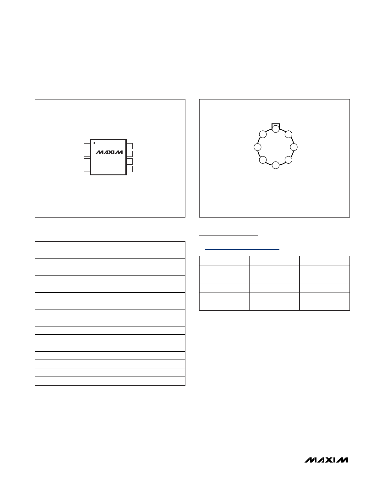
_________________Pin Configurations
TOP VIEW
V+
MAX8211
MAX8212
N.C.
N.C.
GND
8
7
6
5
2
3
4
N.C.
1
HYST
THRESH
OUT
DIP/SO
___________Typical Operating Circuit
19-0539; Rev 5; 9/08
Ordering Information continued on last page.
*
Contact factory for dice specifications.
**
Contact factory for availability and processing to MIL-STD-883.
For pricing, delivery, and ordering information, please contact Maxim Direct at 1-888-629-4642,
or visit Maxim’s website at www.maxim-ic.com.
Pin Configurations continued at end of data sheet.
PART TEMP RANGE
MAX8211CPA -0°C to +70°C 8 Plastic DIP
MAX8211CSA -0°C to +70°C 8 SO
MAX8211CUA -0°C to +70°C 8 µMAX
MAX8211CTY -0°C to +70°C 8 TO-99
MAX8211EPA -40°C to +85°C 8 Plastic DIP
MAX8211ESA -40°C to +85°C 8 SO
MAX8211EJA -40°C to +85°C 8 CERDIP
MAX8211ETY -40°C to +85°C 8 TO-99
MAX8211MJA -55°C to +125°C 8 CERDIP**
PIN PA C K A G E
V+
R3
R2
R1
LOGIC-SUPPLY UNDERVOLTAGE DETECTOR
(DETAILED CIRCUIT DIAGRAM—FIGURE 5)
HYST
THRESH
V+
OUT
MAX8211
GND
µP
NMI
Page 2
MAX8211/MAX8212
Microprocessor Voltage Monitors
with Programmable Voltage Detection
2 _______________________________________________________________________________________
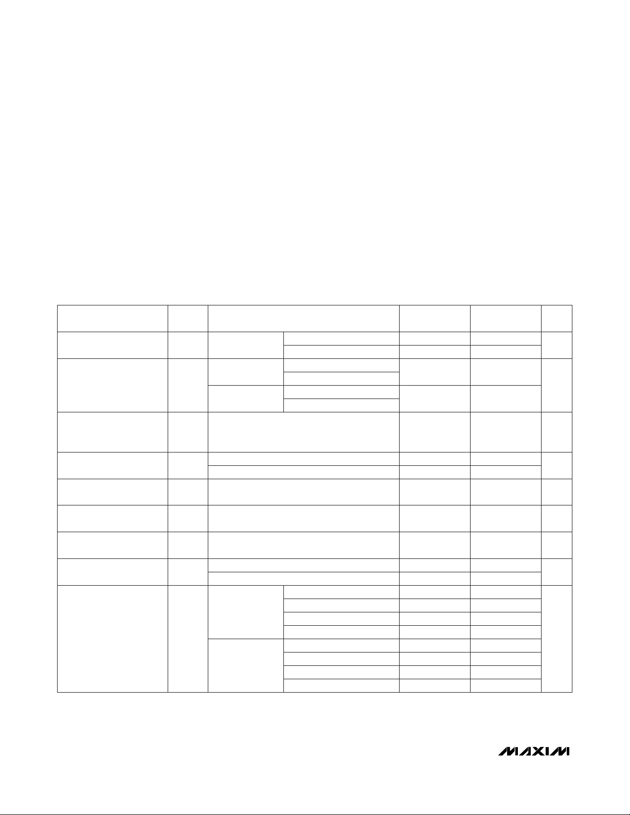
Supply Voltage .......................................................-0.5V to +18V
Output Voltage .......................................................-0.5V to +18V
Hysteresis...................+0.5V to -18V with respect to (V+ + 0.5V)
Threshold Input Voltage ...............................-0.5V to (V+ + 0.5V)
Current into Any Terminal .................................................±50mA
Continuous Power Dissipation (T
A
= +70°C)
8-Pin Plastic DIP (derate 9.09mW/°C above +70°C) .....727mW
8-Pin SO (derate 5.88mW/°C above +70°C)..................471mW
8-Pin CERDIP (derate 8.00mW/°C above +70°C)..........640mW
8-Pin TO-99 (derate 6.67mW/°C above +70°C).............533mW
Operating Temperature Ranges
MAX821_C_ _ .......................................................0°C to +70°C
MAX821_E_ _.....................................................-40°C to +85°C
MAX821_M_ _..................................................-55°C to +125°C
Storage Temperature Range .............................-65°C to +150°C
Lead Temperature (soldering, 10s) .................................+300°C
Stresses beyond those listed under “Absolute Maximum Ratings” may cause permanent damage to the device. These are stress ratings only, and functional
operation of the device at these or any other conditions beyond those indicated in the operational sections of the specifications is not implied. Exposure to
absolute maximum rating conditions for extended periods may affect device reliability.
ABSOLUTE MAXIMUM RATINGS
ELECTRICAL CHARACTERISTICS
(V+ = 5V, TA= +25°C, unless otherwise noted.)
PARAMETER
SYMBOL CONDITIONS UNITS
TA= +25°C 515 515
Supply Current I+
2V ≤ V+ ≤ 16.5V,
GND ≤ V
TH
≤ V+
TA= T
MIN
to T
MAX
20 20
µA
Threshold Voltage
Disparity between Output
and Hysteresis Output
V
THP
±0.1 ±0.1 mV
2.0 16.5 2.0 16.5
Guaranteed Operating
Supply Voltage Range
V
SUPP
2.2 16.5 2.2 16.5
V
Typical Operating
Supply Voltage Range
V
SUPP
1.5 16.5 1.5 16.5 V
Threshold Voltage
Temperature Coefficient
∆V
TH/∆T
-200 -200 ppm/°C
Variation of Threshold
Voltage with Supply Voltage
∆V
TH
V+ = 4.5V to 5.5V 1.0 0.2 mV
0.01 10 0.01 10
Threshold Input Current I
TH
20 20
nA
Output Leakage Current I
LOUT
V
OUT
= 16.5V, VTH= 1.0V 10
V
OUT
= 16.5V, VTH= 1.3V 10
V
OUT
= 5V, VTH= 1.0V 1
TA= T
MIN
to T
MAX
,
C/E temp. ranges
V
OUT
= 5V, VTH= 1.3V 1
V
OUT
= 16.5V, VTH= 0.9V 30
V
OUT
= 16.5V, VTH= 1.3V 30
V
OUT
= 5V, VTH= 0.9V 10
TA= T
MIN
to T
MAX
,
M temp. range
V
OUT
= 5V, VTH= 1.3V 10
µA
MAX8212
MIN TYP MAX
MAX8211
MIN TYP MAX
TA= T
MIN
to T
MAX
0V ≤ VTH≤ V+, TA= +25°C
I
OUT
= 4mA,
I
HYST
= 1mA
TA= +25°C
TA= T
MIN
to T
MAX
See Figure 4
V+ = 16.5V, I
OUT
= 3mA
1.05 1.25 1.05 1.25
V+ = 16.5V, I
OUT
= 4mA
1.11 1.19 1.11 1.19
Threshold Trip Voltage V
TH
TA= +25°C
V+ = 2V, I
OUT
= 500µA
V
TA= T
MIN
to T
MAX
V+ = 2.2V, I
OUT
= 500µA
Page 3
MAX8211/MAX8212
Microprocessor Voltage Monitors
with Programmable Voltage Detection
________________________________________________________________________________________ 3
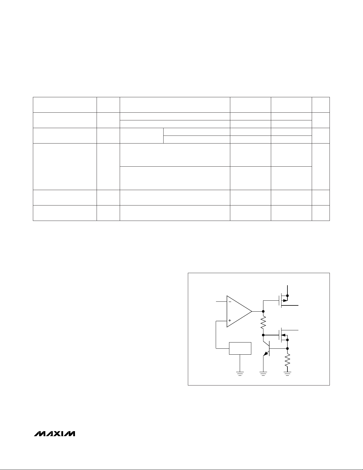
Note 1: The maximum output current of the MAX8211 is limited by design to 30mA under any operating condition. The output voltage
may be sustained at any voltage up to +16.5V as long as the maximum power dissipation of the device is not exceeded.
Note 2: The maximum output current of the MAX8212 is not defined, and systems using the MAX8212 must therefore ensure that the
output current does not exceed 50mA and that the maximum power dissipation of the device is not exceeded.
ELECTRICAL CHARACTERISTICS (continued)
(V+ = 5V, TA= +25°C, unless otherwise noted.)
PARAMETER
SYMBOL CONDITIONS UNITS
I
OUT
= 2mA, VTH= 1.0V 0.17 0.4
Output Saturation Voltage V
OL
I
OUT
= 2mA, VTH= 1.3V 0.17 0.4
V
VTH= 1.0V (Note 1) 4 7.0
Maximum Available
Output Current
I
OH
C temp. range,
V
OUT
= 5V
VTH= 1.3V (Note 2) 12 35
mA
TA= T
MIN
to T
MAX
, C/E temp. ranges,
V+ = 16.5V, VTH= 1.0V,
V
HYST
= -16.5V with respect to V+
0.1 0.1
Hysteresis Leakage
Current
I
LHYS
TA= T
MIN
to T
MAX
, M temp. range,
V+ = 16.5V, V
TH
= 0.9V,
V
HYST
= -16.5V with respect to V+
3 3
µA
Hysteresis Saturation
Voltage
V
HYS
(MAX)
I
HYST
= 0.5mA, VTH= 1.3V,
measured with respect to V+
-0.1 -0.2 -0.1 -0.2 V
Maximum Available
Hysteresis Current
V
HYS
(MAX)
VTH= 1.3V, V
HYS
= 0V 210 210 mA
MAX8212
MIN TYP MAX
MAX8211
MIN TYP MAX
_______________Detailed Description
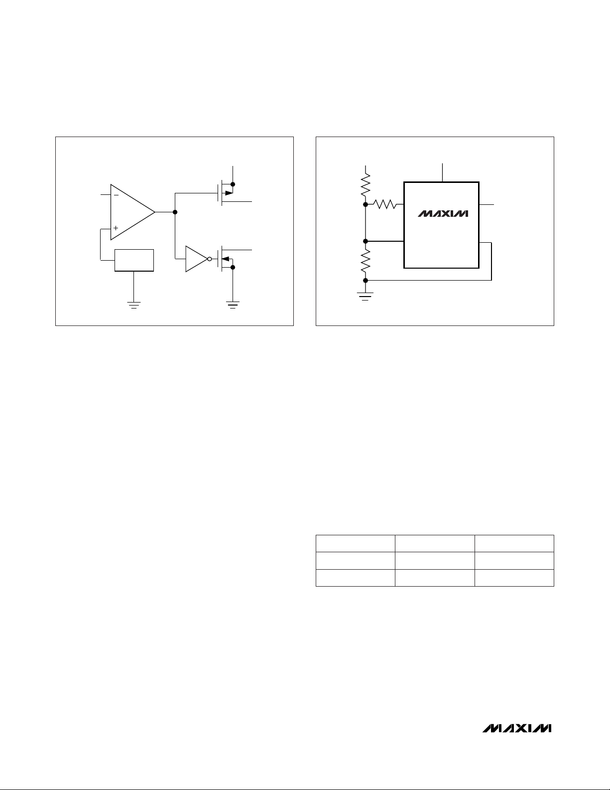
As shown in the block diagrams of Figures 1 and 2, the
MAX8211 and MAX8212 each contain a 1.15V reference, a comparator, an open-drain n-channel output
transistor, and an open-drain p-channel hysteresis output. The MAX8211 output n-channel turns on when the
voltage applied to the THRESH pin is less than the
internal reference (1.15V). The sink current is limited to
7mA (typical), allowing direct drive of an LED without a
series resistor. The MAX8212 output turns on when the
voltage applied to THRESH is greater than the internal
reference. It is not current limited, and will typically sink
35mA.
Compatibility with ICL8211/ICL8212
The CMOS MAX8211/MAX8212 are plug-in replacements
for the bipolar ICL8211/ICL8212 in most applications.
The use of CMOS technology has several advantages.
The quiescent supply current is much less than in the
bipolar parts. Higher-value resistors can also be used
Figure 1. MAX8211 Block Diagram
THRESH
1.15V
REFERENCE
V+
P
HYST
OUT
N
Page 4
MAX8211/MAX8212
Microprocessor Voltage Monitors
with Programmable Voltage Detection
4 ________________________________________________________________________________________
Figure 3. Basic Overvoltage/Undervoltage Circuit
in the networks that set up the trip voltage, since the
comparator input (THRESH pin) is a low-leakage
MOSFET transistor. This further reduces system current
drain. The tolerance of the internal reference has also
been significantly improved, allowing for more precise
voltage detection without the use of potentiometers.
The available current from the HYST output has been
increased from 21µA to 10mA, making the hysteresis
feature easier to use. The disparity between the HYST
output and the voltage required at THRESH to switch
the OUT pin has also been reduced in the MAX8211
from 8mV to 0.1mV to eliminate output “chatter” or
oscillation.
Most voltage detection circuits operate with supplies of
15V or less; in these applications, the MAX8211/
MAX8212 will replace ICL8211/ICL8212s with the performance advantages described above. However, note
that the CMOS parts have an absolute maximum supply-voltage rating of 18V, and should never be used in
applications where this rating could be exceeded.
Exercise caution when replacing ICL8211/ICL8212s in
closed-loop applications such as programmable
zeners. Although neither the ICL8211/ICL8212 nor the
MAX8211/MAX8212 are internally compensated, the
CMOS parts have higher gain and may not be stable
for the external compensation-capacitor values used in
lower-gain ICL8211/ICL8212 circuits.
__________Applications Information
Basic Voltage Detectors
Figure 3 shows the basic circuit for both undervoltage
detection (MAX8211) and overvoltage detection
(MAX8212). For applications where no hysteresis is
needed, R3 should be omitted. The ratio of R1 to R2 is
then chosen such that, for the desired trip voltage at VIN,
1.15V is applied to the THRESH pin. Since the comparator inputs are very low-leakage MOSFET transistors, the MAX8211/MAX8212 can use much higher
resistors values in the attenuator network than can the
bipolar ICL8211/ICL8212. See Table 1 for switching
delays.
Table 1. Switching Delays
Voltage Detectors with Hysteresis
To ensure noise-free output switching, hysteresis is
frequently used in voltage detectors. For both the
MAX8211 and MAX8212 the HYST output is on for
threshold voltages greater than 1.15V. R3 (Figure 3)
controls the amount of current (positive feedback) supplied from the HYST output to the mid-point of the resistor divider, and hence the magnitude of the hysteresis,
or dead-band.
Figure 2. MAX8212 Block Diagram
TYPICAL DELAYS MAX8211 MAX8212
t
(on)
40µs 250µs
t
(off)
1.5ms 3ms
V+
THRESH
1.15V
REFERENCE
P
N
HYST
OUT
V
IN
R2
R1
R3
HYST
THRESH
V+
V+
MAX8211
MAX8212
OUT
GND
V
OUT
Page 5
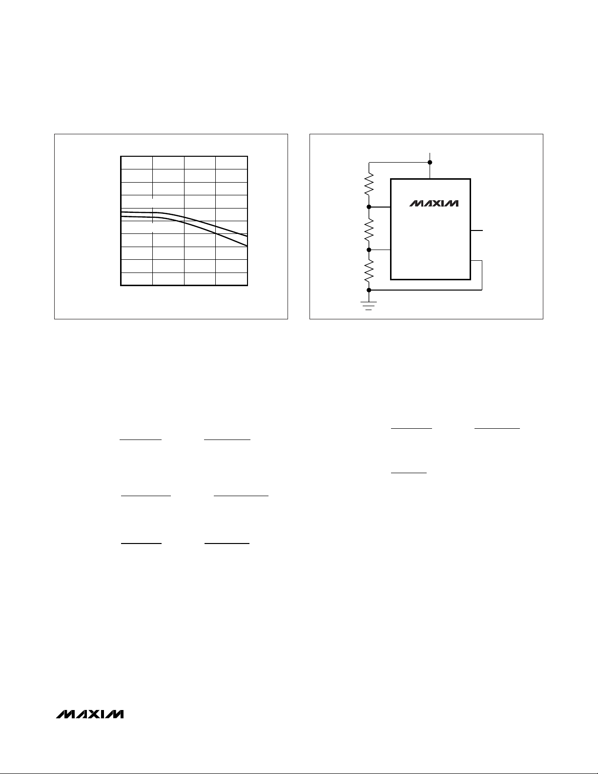
Calculate resistor values for Figure 3 as follows:
1) Choose a value for R1. Typical values are in
the 10kΩ to 10MΩ range.
2) Calculate R2 for the desired upper trip point
VUusing the formula:
3) Calculate R3 for the desired amount of
hysteresis, where VL is the lower trip point:
or, if V+ = VIN:
Figure 5 shows an alternate circuit, suitable only when the
voltage being detected is also the power-supply voltage
for the MAX8211 or MAX8212.
Calculate resistor values for Figure 5 as follows:
1) Choose a value for R1. Typical values are in
the 10kΩ to 10MΩ range.
2) Calculate R2:
3) Calculate R3:
Low-Voltage Detector for Logic Supply
The circuit of Figure 5 will detect when a 5.0V (nominal)
supply goes below 4.5V, which is the V
MIN
normally
specified in logic systems. The selected resistor values
ensure that false undervoltage alarms will not be generated, even with worst-case threshold trip values and
resistor tolerances. R3 provides approximately 75mV of
hysteresis.
MAX8211/MAX8212
Microprocessor Voltage Monitors
with Programmable Voltage Detection
________________________________________________________________________________________ 5
Figure 4. MAX8211/MAX8212 Threshold Trip Voltage vs.
Ambient Temperature
Figure 5. MAX8211 Logic-Supply Low-Voltage Detector
1.250
1.230
(V)
TH
V
1.210
1.190
1.170
1.150
1.130
1.110
1.090
1.070
1.050
-55
V+ = 16.5V
V+ = 2V
-25 25 75 125
T
(°C)
A
MAX8211,8212-FIG 4
R2 = R1
(VUVTH)
−
×
V
TH
=×
R1
(VU1.15V)
−
1.15V
R3 R2
=×
R3 R2
=×
(V VTH)
+−
(VUVL)
−
(VLVTH)
−
(VUVL)
−
=×
R2
=×
R2
(VL1.15V)
(V + 1.15V)
(VUVL)
−
(VUVL)
−
−
−
V
IN
R3
48.7k
2.2M
750k
1%
1%
Ω
R2
Ω
1%
HYST
THRESH
R1
Ω
V+
MAX8211
OUT
GND
V
OUT
(LOW FOR
< 4.5V)
V
IN
R2 R1
=×
R3 R1
=×
(VLVTH)
−
V
TH
(VUVL)
−
1.15V
=×
R1
(VL1.15V)
1.15V
−
Page 6
MAX8211/MAX8212
Microprocessor Voltage Monitors
with Programmable Voltage Detection
6 _______________________________________________________________________________________
_Ordering Information (continued)
_____________________________________________Pin Configurations (continued)
*
Contact factory for dice specifications.
**
Contact factory for availability and processing to MIL-STD-883.
Package Information
For the latest package outline information and land patterns, go
to www.maxim-ic.com/packages
.
PACKAGE TYPE PACKAGE CODE DOCUMENT NO.
8 CERDIP J8-2
21-0045
8 Plastic DIP P8-1
21-0043
8 SO S8-2
21-0041
8 TO-99 T99-8
21-0022
8 µMAX U8-1
21-0036
TOP VIEW
OUT
N.C.
N.C.
GND
1
2
MAX8211
3
MAX8212
4
µ
MAX
8
7
6
5
THRESH
HYST
N.C.
V+
PART TEMP RANGE
MAX8211MSA/PR -55°C to +125°C 8 SO**
MAX8211MSA/PR-T -55°C to +125°C 8 SO**
MAX8211MTV -55°C to +125°C 8 TO-99**
MAX8212CPA -0°C to +70°C 8 Plastic DIP
MAX8212CSA -0°C to +70°C 8 SO
MAX8212CUA -0°C to +70°C 8 µMAX
MAX8212CTY -0°C to +70°C 8 TO-99
MAX8212EPA -40°C to +85°C 8 Plastic DIP
MAX8212ESA -40°C to +85°C 8 SO
MAX8212EJA -40°C to +85°C 8 CERDIP
MAX8212ETY -40°C to +85°C 8 TO-99
MAX8212MJA -55°C to +125°C 8 CERDIP**
MAX8212MSA/PR -55°C to +125°C 8 SO**
MAX8212MSA/PR-T -55°C to +125°C 8 SO**
MAX8212MTV -55°C to +125°C 8 TO-99**
PIN PA C K A G E
TOP VIEW
HYST
V+
7
6
N.C.
5
N.C.
2
1
3
TO-99*
8
4
GND
THRESH
OUT
N.C.
*
CASE IS CONNECTED TO PIN 7 ON TV PACKAGE.
CASE IS CONNECTED TO PIN 4 ON TY PACKAGE.
Page 7

Maxim cannot assume responsibility for use of any circuitry other than circuitry entirely embodied in a Maxim product. No circuit patent licenses are
implied. Maxim reserves the right to change the circuitry and specifications without notice at any time.
7
___________________Maxim Integrated Products, 120 San Gabriel Drive, Sunnyvale, CA 94086 (408) 737-7600
© 2008 Maxim Integrated Products is a registered trademark of Maxim Integrated Products, Inc.
MAX8211/MAX8212
Microprocessor Voltage Monitors
with Programmable Voltage Detection
Revision History
REVISION
NUMBER
0 1/91 Initial release —
4 9/02 Updated Figure 5. 5
5 9/08 Updated Ordering Information. 1, 6
REVISION
DATE
DESCRIPTION
PAGES
CHANGED
 Loading...