

Page 1
General Description
The MAX803/MAX809/MAX810 are microprocessor (µP)
supervisory circuits used to monitor the power supplies
in µP and digital systems. They provide excellent circuit
reliability and low cost by eliminating external components and adjustments when used with +5V, +3.3V,
+3.0V, or +2.5V powered circuits.
These circuits perform a single function: they assert a
reset signal whenever the VCCsupply voltage declines
below a preset threshold, keeping it asserted for at
least 140ms after VCChas risen above the reset threshold. Reset thresholds suitable for operation with a variety of supply voltages are available.
The MAX803 has an open-drain output stage, while the
MAX809/MAX810 have push-pull outputs. The
MAX803’s open-drain RESET output requires a pull-up
resistor that can be connected to a voltage higher than
VCC. The MAX803/MAX809 have an active-low RESET
output, while the MAX810 has an active-high RESET
output. The reset comparator is designed to ignore fast
transients on VCC, and the outputs are guaranteed to
be in the correct logic state for VCCdown to 1V.
Low supply current makes the MAX803/MAX809/
MAX810 ideal for use in portable equipment. The
MAX803 is available in a 3-pin SC70 package, and the
MAX809/MAX810 are available in 3-pin SC70 or SOT23
packages.
Applications
Computers
Controllers
Intelligent Instruments
Critical µP and µC Power Monitoring
Portable/Battery-Powered Equipment
Automotive
____________________________Features
♦ Precision Monitoring of +2.5V, +3V, +3.3V, and
+5V Power-Supply Voltages
♦ Fully Specified Over Temperature
♦ Available in Three Output Configurations
Open-Drain RESET Output (MAX803)
Push-Pull RESET Output (MAX809)
Push-Pull RESET Output (MAX810)
♦ 140ms min Power-On Reset Pulse Width
♦ 12µA Supply Current
♦ Guaranteed Reset Valid to VCC= +1V
♦ Power Supply Transient Immunity
♦ No External Components
♦ 3-Pin SC70 and SOT23 Packages
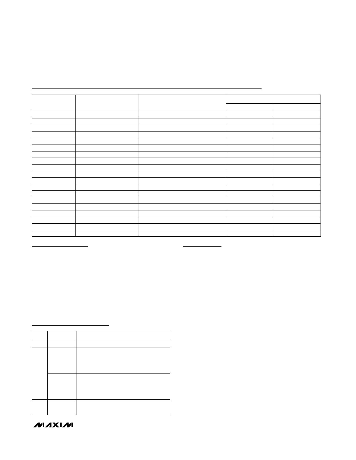
MAX803L/M/R/S/T/Z, MAX809J/L/M/R/S/T/Z, MAX810L/M/R/S/T/Z
3-Pin Microprocessor Reset Circuits
________________________________________________________________ Maxim Integrated Products 1
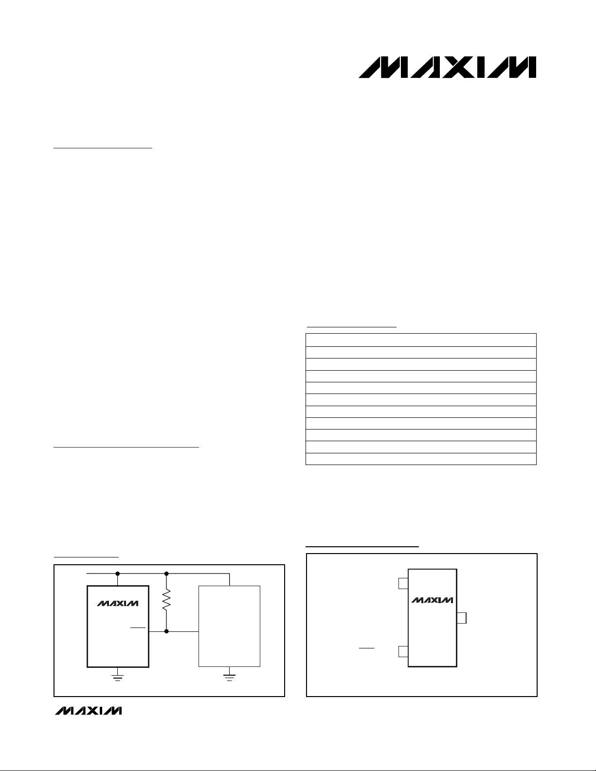
Pin Configuration
Typical Operating Circuit
19-0344; Rev 5; 1/01
Note: These parts are offered in 2.5k or 10k reels, and must be
ordered in 2.5k or 10k increments. Order MAX803_EXR-T for
2.5k reels and MAX803_EXR-T10 for 10k reels. Insert the
desired suffix letter from the Selector Guide into the blank to
complete the part number. All versions of these products may
not be available at the time of announcement. Contact factory for
availability.
3 SC70-3-40°C to +125°CMAX803_EXR-T10
3 SC70-3
PIN-PACKAGETEMP. RANGE
-40°C to +125°C
MAX803_EXR-T
PART
3 SC70-3-40°C to +125°CMAX809_EXR-T10
3 SC70-3-40°C to +125°C
MAX809_EXR-T
3 SOT23-3-40°C to +105°CMAX809_EUR-T10
3 SOT23-3-40°C to +105°CMAX809_EUR-T
3 SC70-3-40°C to +125°CMAX810_EXR-T10
3 SC70-3-40°C to +125°C
MAX810_EXR-T
3 SOT23-3-40°C to +105°CMAX810_EUR-T10
3 SOT23-3-40°C to +105°CMAX810_EUR-T
Ordering Information
For pricing, delivery, and ordering information, please contact Maxim/Dallas Direct! at
1-888-629-4642, or visit Maxim’s website at www.maxim-ic.com.
V
CC
RESET
INPUT
V
CC
µP
V
CC
MAX803
MAX809
RESET
R
PULL-UP
*
TOP VIEW
1
GND
MAX803
MAX809
MAX810
V
3
CC
2
SC70-3/SOT23-3
*MAX803 ONLY
GND
GND
( ) ARE FOR MAX810.
MAX803 AVAILABLE IN SC70-3 ONLY.
RESET (RESET)
Page 2
MAX803L/M/R/S/T/Z, MAX809J/L/M/R/S/T/Z, MAX810L/M/R/S/T/Z
3-Pin Microprocessor Reset Circuits
2 _______________________________________________________________________________________
ABSOLUTE MAXIMUM RATINGS
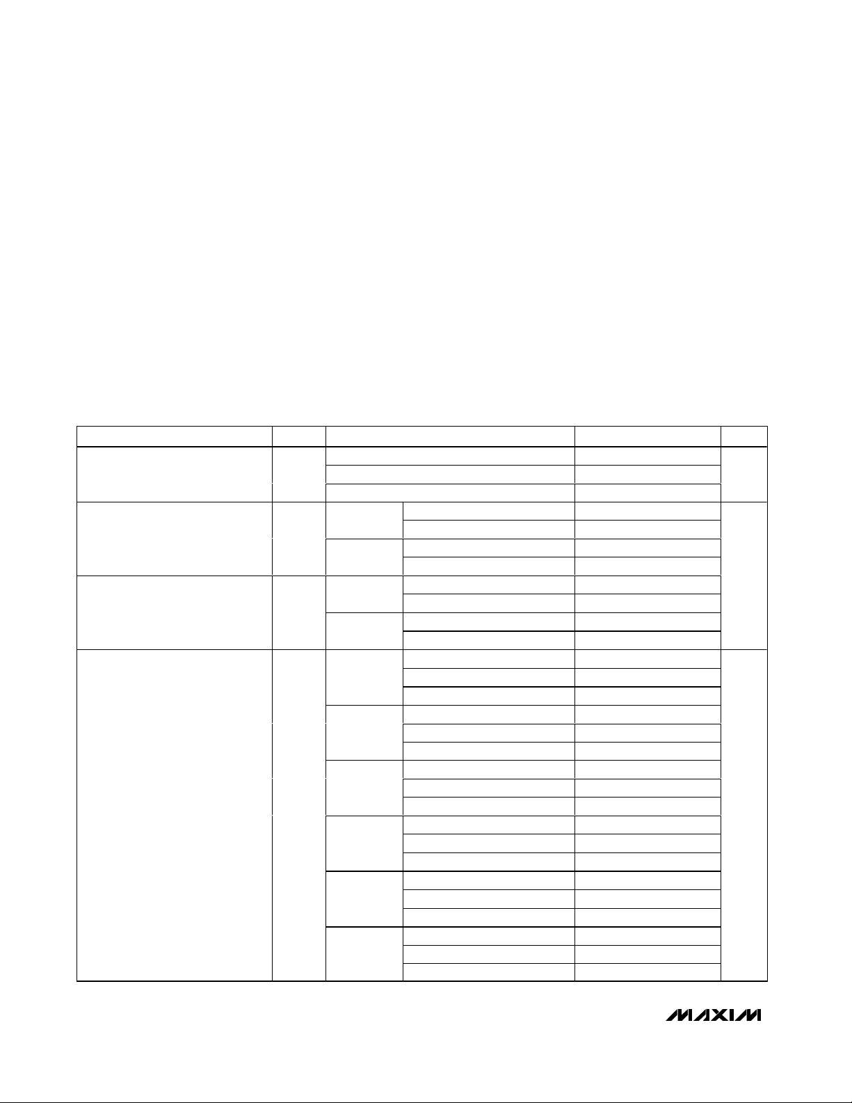
ELECTRICAL CHARACTERISTICS
(VCC= full range, TA= -40°C to +105°C (SOT23) or TA= -40°C to +125°C (SC70), unless otherwise noted. Typical values are at TA=
+25°C, V
CC
= 5V for L/M/J versions, VCC= 3.3V for T/S versions, VCC= 3V for R version, and VCC= 2.5V for Z version.) (Note 1)
Stresses beyond those listed under “Absolute Maximum Ratings” may cause permanent damage to the device. These are stress ratings only, and functional
operation of the device at these or any other conditions beyond those indicated in the operational sections of the specifications is not implied. Exposure to
absolute maximum rating conditions for extended periods may affect device reliability.
Terminal Voltage (with respect to GND)
V
CC
....................................................................-0.3V to +6.0V
RESET, RESET (push-pull) .....................-0.3V to (V
CC
+ 0.3V)
RESET (open drain)...........................................-0.3V to +6.0V
Input Current, V
CC
..............................................................20mA
Output Current, RESET, RESET ..........................................20mA
Rate of Rise, V
CC
............................................................100V/µs
Continuous Power Dissipation (T
A
= +70°C)
3-Pin SC70 (derate 2.17mW/°C above +70°C)............174mW
3-Pin SOT23 (derate 4mW/°C above +70°C)...............320mW
Operating Temperature Range
3-Pin SC70.....................................................-40°C to +125°C
3-Pin SOT23...................................................-40°C to +105°C
Storage Temperature Range .............................-65°C to +150°C
Lead Temperature (soldering, 10s) .................................+300°C
VCC Range
Supply Current (SOT23) I
Supply Current (SC70) I
Reset Threshold
(SOT only)
PARAMETER SYMBOL CONDITIONS MIN TYP MAX UNITS
TA = 0°C to +70°C 1.0 5.5
TA = -40°C to +105°C (MAX8_ _ _EUR) 1.2 5.5
= -40°C to +125°C (MAX8_ _ _EXR) 1.2 5.5
T
A
TA = -40°C
to +85°C
CC
TA = +85°C
to +105°C
TA = -40°C
to +85°C
CC
TA = +85°C
to +125°C
MAX8_ _L
MAX809J
(SOT only)
V
TH
MAX8_ _T
MAX8_ _R
VCC < 5.5V, MAX8_ _L/M 24 60
< 3.6V, MAX8_ _R/S/T/Z 17 50
V
CC
VCC < 5.5V, MAX8_ _L/M 100
V
< 3.6V, MAX8_ _R/S/T/Z 100
CC
VCC < 5.5V, MAX8_ _L/M 24 35
V
< 3.6V, MAX8_ _R/S/T/Z 17 30
CC
VCC < 5.5V, MAX8_ _L/M 60
V
< 3.6V, MAX8_ _R/S/T/Z 60
CC
TA = +25°C 4.56 4.63 4.70
TA = -40°C to +85°C 4.50 4.75
= -40°C to +125°C 4.40 4.86
T
A
TA = +25°C 4.31 4.38 4.45
TA = -40°C to +85°C 4.25 4.50MAX8_ _M
T
= -40°C to +125°C 4.16 4.56
A
TA = +25°C 3.93 4.00 4.06
TA = -40°C to +85°C 3.89 4.10
= -40°C to +125°C 3.80 4.20
T
A
TA = +25°C 3.04 3.08 3.11
TA = -40°C to +85°C 3.00 3.15
= -40°C to +125°C 2.92 3.23
T
A
TA = +25°C 2.89 2.93 2.96
TA = -40°C to +85°C 2.85 3.00MAX8_ _S
= -40°C to +125°C 2.78 3.08
T
A
TA = +25°C 2.59 2.63 2.66
TA = -40°C to +85°C 2.55 2.70
= -40°C to +125°C 2.50 2.76
T
A
V
µA
V
Page 3
MAX803L/M/R/S/T/Z, MAX809J/L/M/R/S/T/Z, MAX810L/M/R/S/T/Z
3-Pin Microprocessor Reset Circuits
_______________________________________________________________________________________ 3
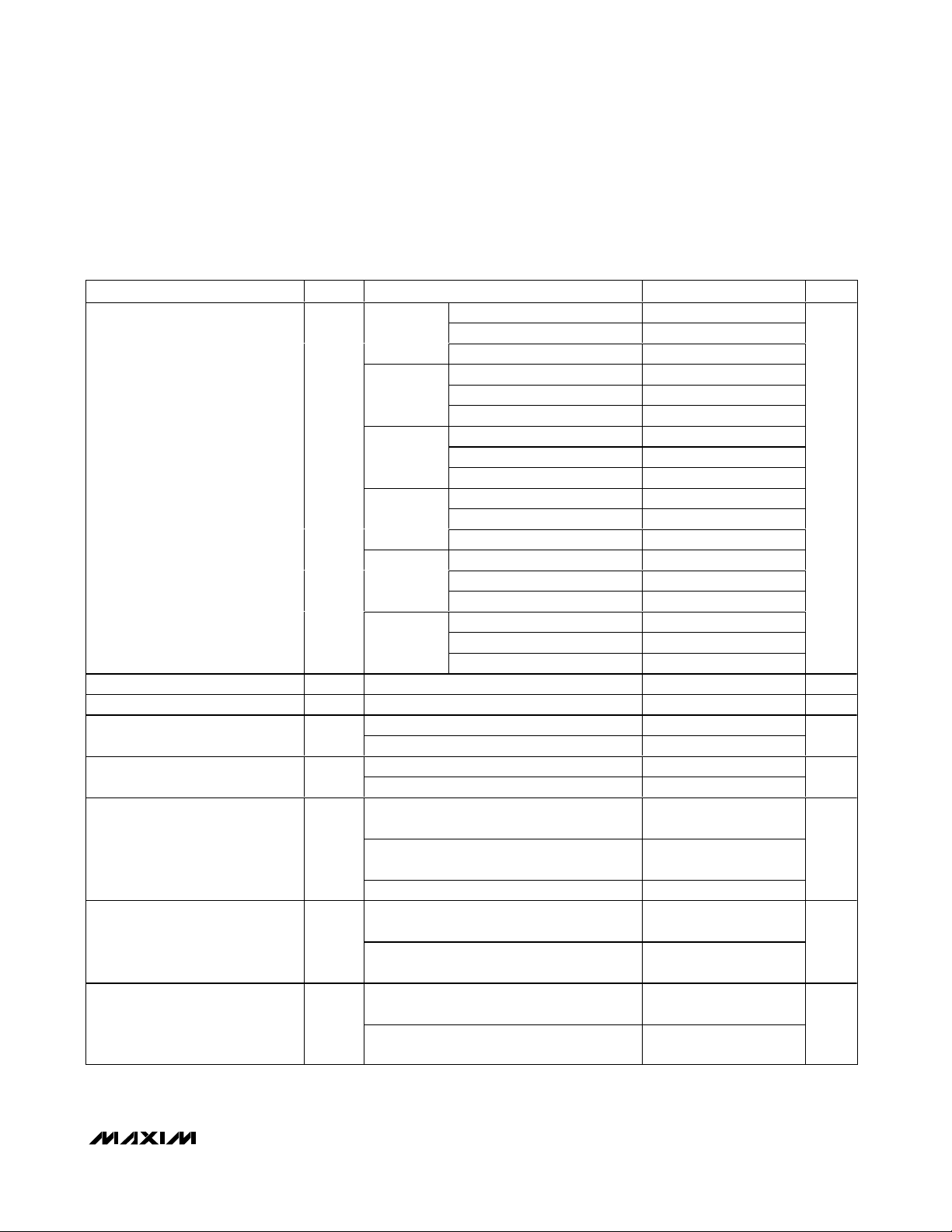
ELECTRICAL CHARACTERISTICS (continued)
(VCC= full range, TA= -40°C to +105°C (SOT23) or TA= -40°C to +125°C (SC70), unless otherwise noted. Typical values are at TA=
+25°C, V
CC
= 5V for L/M/J versions, VCC= 3.3V for T/S versions, VCC= 3V for R version, and VCC= 2.5V for Z version.) (Note 1)
Reset Threshold
(SC70 only)
Reset Threshold Tempco 30 ppm/°C
VCC to Reset Delay (Note 2) VCC = VTH to (VTH - 100 mV) 20 µs
Reset Active Timeout Period
(SOT23)
Reset Active Timeout Period
(SC70)
RESET Output Voltage Low (pushpull active low and open-drain
active low, MAX803 and MAX809)
RESET Output Voltage High
(push-pull active low MAX809)
RESET Output Voltage Low (pushpull active high, MAX810)
PARAMETER SYMBOL CONDITIONS MIN TYP MAX UNITS
TA = +25°C 4.56 4.63 4.70
MAX8_ _L
MAX8_ _T
V
TH
MAX8_ _S
MAX8_ _Z
(SC70 only)
TA = -40°C to +85°C 140 240 560
= +85°C to +105°C 100 840
T
A
TA = -40°C to +85°C 140 240 460
= +85°C to +125°C 100 840
T
A
VCC = VTH min, I
MAX803R/S/T/Z, MAX809R/S/T/Z
V
OL
VCC = VTH min, I
MAX803L/M, MAX809J/L/M
VCC > 1.0V, I
VCC > VTH max, I
V
V
MAX803R/S/T/Z, MAX809R/S/T/Z
OH
VCC > VTH max, I
MAX803L/M, MAX809J/L/M
VCC = VTH max, I
MAX810R/S/T/Z
OL
VCC = VTH max, I
MAX810L/M
TA = -40°C to +85°C 4.50 4.75
= -40°C to +125°C 4.44 4.82
T
A
TA = +25°C 4.31 4.38 4.45
TA = -40°C to +85°C 4.25 4.50MAX8_ _M
= -40°C to +125°C 4.20 4.56
T
A
TA = +25°C 3.04 3.08 3.11
TA = -40°C to +85°C 3.00 3.15
= -40°C to +125°C 2.95 3.21
T
A
TA = +25°C 2.89 2.93 2.96
TA = -40°C to +85°C 2.85 3.00
= -40°C to +125°C 2.81 3.05
T
A
TA = +25°C 2.59 2.63 2.66
TA = -40°C to +85°C 2.55 2.70MAX8_ _R
= -40°C to +125°C 2.52 2.74
T
A
TA = +25°C 2.28 2.32 2.35
TA = -40°C to +85°C 2.25 2.38
T
= -40°C to +125°C 2.22 2.42
A
= 1.2mA,
SINK
= 3.2mA,
SINK
= 50µA 0.3
SINK
= 500µA,
SOURCE
SOURCE
= 1.2mA,
SINK
= 3.2mA,
SINK
= 800µA,
0.8V
V
CC
CC
- 1.5
0.3
0.4
0.3
0.4
V
ms
ms
V
V
V
Page 4
MAX803L/M/R/S/T/Z, MAX809J/L/M/R/S/T/Z, MAX810L/M/R/S/T/Z
3-Pin Microprocessor Reset Circuits
4 _______________________________________________________________________________________
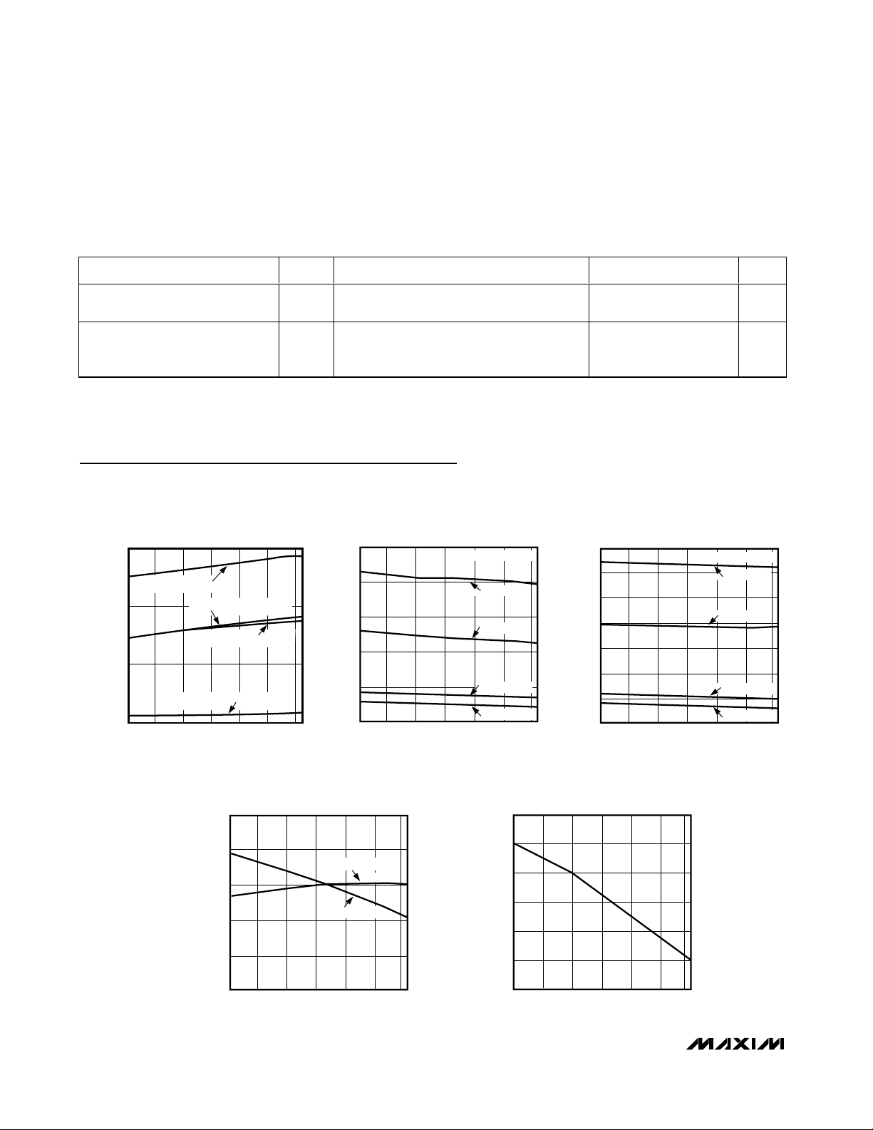
Typical Operating Characteristics
(VCC= full range, TA= -40°C to +105°C, unless otherwise noted. Typical values are at TA= +25°C, VCC= +5V for L/M/J versions,
V
CC
= +3.3V for T/S versions, VCC= +3V for R version, and VCC= +2.5V for Z version.)
-40 20 40
-20 0 60 85
SUPPLY CURRENT vs. TEMPERATURE
(SC70 PACKAGE, NO LOAD)
MAX803 toc01
TEMPERATURE (°C)
SUPPLY CURRENT (µA)
0
5
10
15
MAX8_ _R/S/T, VCC = 3.3V
MAX8_ _L/M/R/S/T/Z, VCC = 1V
MAX8_ _Z, VCC = 2.5V
MAX8_ _L/M, VCC = 5V
ELECTRICAL CHARACTERISTICS (continued)
(VCC= full range, TA= -40°C to +105°C (SOT23) or TA= -40°C to +125°C (SC70), unless otherwise noted. Typical values are at TA=
+25°C, V
CC
= 5V for L/M/J versions, VCC= 3.3V for T/S versions, VCC= 3V for R version, and VCC= 2.5V for Z version.) (Note 1)
Note 1: Production testing done at TA= +25°C; limits over temperature guaranteed by design only.
Note 2: RESET output for MAX803/MAX809; RESET output for MAX810.
Note 3: Guaranteed by design, not production tested.
RESET Output Voltage High
(push-pull active high, MAX810)
RESET Open-Drain Output
Leakage Current (MAX803)
(Note 3)
PARAMETER SYMBOL CONDITIONS MIN TYP MAX UNITS
V
1.8V < VCC < VTH min, I
OH
V
> VTH, RESET deasserted 1 µA
CC
= 150µA 0.8V
SOURCE
CC
POWER-DOWN RESET DELAY vs.
TEMPERATURE (MAX8_ _R/S/T/Z)
100
80
60
40
20
POWER-DOWN RESET DELAY (µs)
0
-20
-40
0
TEMPERATURE (°C)
20
VOD = VTH - V
VOD = 10mV
VOD = 20mV
VOD = 100mV
VOD = 200mV
60
40
CC
MAX803-TOC3
POWER-DOWN RESET DELAY (µs)
85
POWER-DOWN RESET DELAY vs.
TEMPERATURE (MAX8_ _J/L/M)
140
120
100
80
60
40
20
0
-20
-40
0
TEMPERATURE (°C)
20
= VTH - V
V
OD
VOD = 10mV
VOD = 20mV
VOD = 100mV
VOD = 200mV
40
V
CC
60
MAX803-TOC4
85
POWER-UP RESET TIMEOUT
vs. TEMPERATURE
250
245
240
235
POWER-UP RESET TIMEOUT (ms)
230
225
-40
-20
0
TEMPERATURE (°C)
MAX8_ _J/L/M
MAX8_ _R/S/T/Z
20
40
MAX803-TOC5
85
60
1.003
1.002
1.001
1.000
0.999
NORMALIZED THRESHOLD
0.998
0.997
NORMALIZED RESET THRESHOLD
vs. TEMPERATURE
-40
-20
20
0
TEMPERATURE (°C)
MAX803-TOC6
85
60
40
Page 5
MAX803L/M/R/S/T/Z, MAX809J/L/M/R/S/T/Z, MAX810L/M/R/S/T/Z
_______________________________________________________________________________________ 5
Detailed Description
A microprocessor’s (µP’s) reset input starts the µP in a
known state. The MAX803/MAX809/MAX810 assert
reset to prevent code-execution errors during powerup, power-down, or brownout conditions. They assert a
reset signal whenever the VCCsupply voltage declines
below a preset threshold, keeping it asserted for at
least 140ms after VCChas risen above the reset threshold. The MAX803 uses an open-drain output, and the
MAX809/MAX810 have a push-pull output stage.
Connect a pull-up resistor on the MAX803’s RESET output to any supply between 0 and 6V.
Applications Information
Negative-Going VCCTransients
In addition to issuing a reset to the µP during power-up,
power-down, and brownout conditions, the MAX803/
MAX809/MAX810 are relatively immune to short-duration
negative-going VCCtransients (glitches).
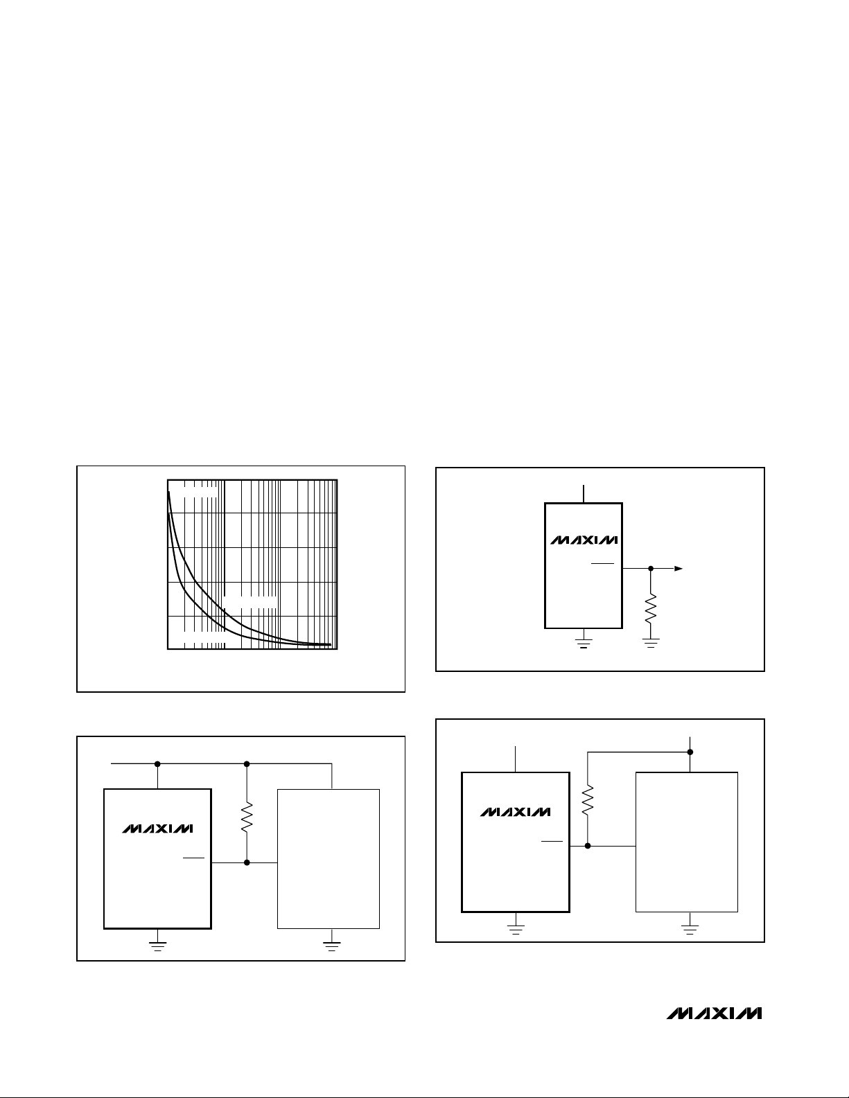
Figure 1 shows typical transient duration vs. reset comparator overdrive, for which the MAX803/MAX809/
MAX810 do not generate a reset pulse. The graph was
generated using a negative-going pulse applied to VCC,
starting 0.5V above the actual reset threshold and ending below it by the magnitude indicated (reset comparator overdrive). The graph indicates the maximum pulse
width a negative-going VCCtransient can have without
causing a reset pulse. As the magnitude of the transient
increases (goes farther below the reset threshold), the
maximum allowable pulse width decreases. Typically, for
the MAX8__L and MAX8__M, a VCCtransient that goes
100mV below the reset threshold and lasts 20µs or less
will not cause a reset pulse. A 0.1µF bypass capacitor
mounted as close as possible to the VCCpin provides
additional transient immunity.
Ensuring a Valid Reset Output
Down to V
CC
= 0
When VCCfalls below 1V, the MAX809 RESET output
no longer sinks current—it becomes an open circuit.
3-Pin Microprocessor Reset Circuits
2
RESET
(MAX803/
MAX809)
RESET Output remains low while V
CC
is below the reset threshold, and for at
least 140ms after V
CC
rises above the
reset threshold.
1 GND Ground
PIN NAME FUNCTION
RESET
(MAX810)
RESET Output remains high while V
CC
is below the reset threshold, and for at
least 140ms after V
CC
rises above the
reset threshold.
3 V
CC
Supply Voltage (+5V, +3.3V, +3.0V, or
+2.5V)
Selector Guide
Pin Description
PART/SUFFIX RESET THRESHOLD (V) OUTPUT TYPE
MAX803L 4.63 OPEN-DRAIN RESET AAZ
MAX803M 4.38 OPEN-DRAIN RESET ABA
MAX803T 3.08 OPEN-DRAIN RESET ABB
MAX803S 2.93 OPEN-DRAIN RESET ABC
MAX803R 2.63 OPEN-DRAIN RESET ABD
MAX803Z 2.32 OPEN-DRAIN RESET ABE
MAX809L 4.63 PUSH-PULL RESET AAAA AAN
MAX809M 4.38 PUSH-PULL RESET ABAA AAO
MAX809J 4.00 PUSH-PULL RESET CWAA
MAX809T 3.08 PUSH-PULL RESET ACAA AAP
MAX809S 2.93 PUSH-PULL RESET ADAA AAQ
MAX809R 2.63 PUSH-PULL RESET AFAA AAR
MAX809Z 2.32 PUSH-PULL RESET AAS
MAX810L 4.63 PUSH-PULL RESET AGAA AAT
MAX810M 4.38 PUSH-PULL RESET AHAA AAU
MAX810T 3.08 PUSH-PULL RESET AJAA AAV
MAX810S 2.93 PUSH-PULL RESET AKAA AAX
MAX810R 2.63 PUSH-PULL RESET ALAA AAW
MAX810Z 2.32 PUSH-PULL RESET AAY
TOP MARK
SOT SC70
Page 6
MAX803L/M/R/S/T/Z, MAX809J/L/M/R/S/T/Z, MAX810L/M/R/S/T/Z
Therefore, high-impedance CMOS logic inputs connected to RESET can drift to undetermined voltages.
This presents no problem in most applications since
most µP and other circuitry is inoperative with V
CC
below 1V. However, in applications where RESET must
be valid down to 0V, adding a pull-down resistor to
RESET causes any stray leakage currents to flow to
ground, holding RESET low (Figure 2). R1’s value is not
critical; 100kΩ is large enough not to load RESET and
small enough to pull RESET to ground.
A 100kΩ pull-up resistor to VCCis also recommended
for the MAX810 if RESET is required to remain valid for
VCC< 1V.
Interfacing to µPs with
Bidirectional Reset Pins
Since the RESET output on the MAX803 is open drain,
this device interfaces easily with µPs that have bidirectional reset pins, such as the Motorola 68HC11.
Connecting the µP supervisor’s RESET output directly
to the microcontroller’s (µC’s) RESET pin with a single
pull-up resistor allows either device to assert reset
(Figure 3).
MAX803 Open-Drain
RESET
Output
Allows Use with Multiple Supplies
Generally, the pull-up connected to the MAX803 will
connect to the supply voltage that is being monitored at
the IC’s V
CC
pin. However, some systems may use the
open-drain output to level-shift from the monitored supply to reset circuitry powered by some other supply
(Figure 4). Note that as the MAX803’s VCCdecreases
3-Pin Microprocessor Reset Circuits
6 _______________________________________________________________________________________
Figure 4. MAX803 Open-Drain
RESET
Output Allows Use with
Multiple Supplies
Figure 3. Interfacing to µPs with Bidirectional Reset I/O
Figure 1. Maximum Transient Duration Without Causing a
Reset Pulse vs. Reset Comparator Overdrive
Figure 2.
RESET
Valid to VCC= Ground Circuit
400
TA = +25°C
320
240
160
MAX8_ _J/L/M
80
MAXIMUM TRANSIENT DURATION (µs)
MAX8_ _R/S/T/Z
0
1 100 1000
RESET COMPARATOR OVERDRIVE, V
10
- VCC (mV)
TH
V
CC
MAX809
RESET
R1
100k
+5.0V
GND
+3.3V
V
CC
RESET
INPUT
V
CC
5V SYSTEM
GND
RESET
INPUT
V
CC
µP
MOTOROLA
68HCXX
GND
V
CC
MAX803
GND
RESET
V
CC
MAX803
RESET
GND
R
PULLUP
Page 7
below 1V, so does the IC’s ability to sink current at
RESET. Also, with any pull-up, RESET will be pulled
high as VCCdecays toward 0. The voltage where this
occurs depends on the pull-up resistor value and the
voltage to which it is connected.
Benefits of Highly Accurate
Reset Threshold
Most µP supervisor ICs have reset threshold voltages
between 5% and 10% below the value of nominal supply voltages. This ensures a reset will not occur within
5% of the nominal supply, but will occur when the supply is 10% below nominal.
When using ICs rated at only the nominal supply ±5%,
this leaves a zone of uncertainty where the supply is
between 5% and 10% low, and where the reset may or
may not be asserted.
The MAX8__L/T/Z use highly accurate circuitry to
ensure that reset is asserted close to the 5% limit, and
long before the supply has declined to 10% below
nominal.
MAX803L/M/R/S/T/Z, MAX809J/L/M/R/S/T/Z, MAX810L/M/R/S/T/Z
3-Pin Microprocessor Reset Circuits
_______________________________________________________________________________________ 7
TRANSISTOR COUNT: 275 (SOT23)
380 (SC70)
___________________Chip Information
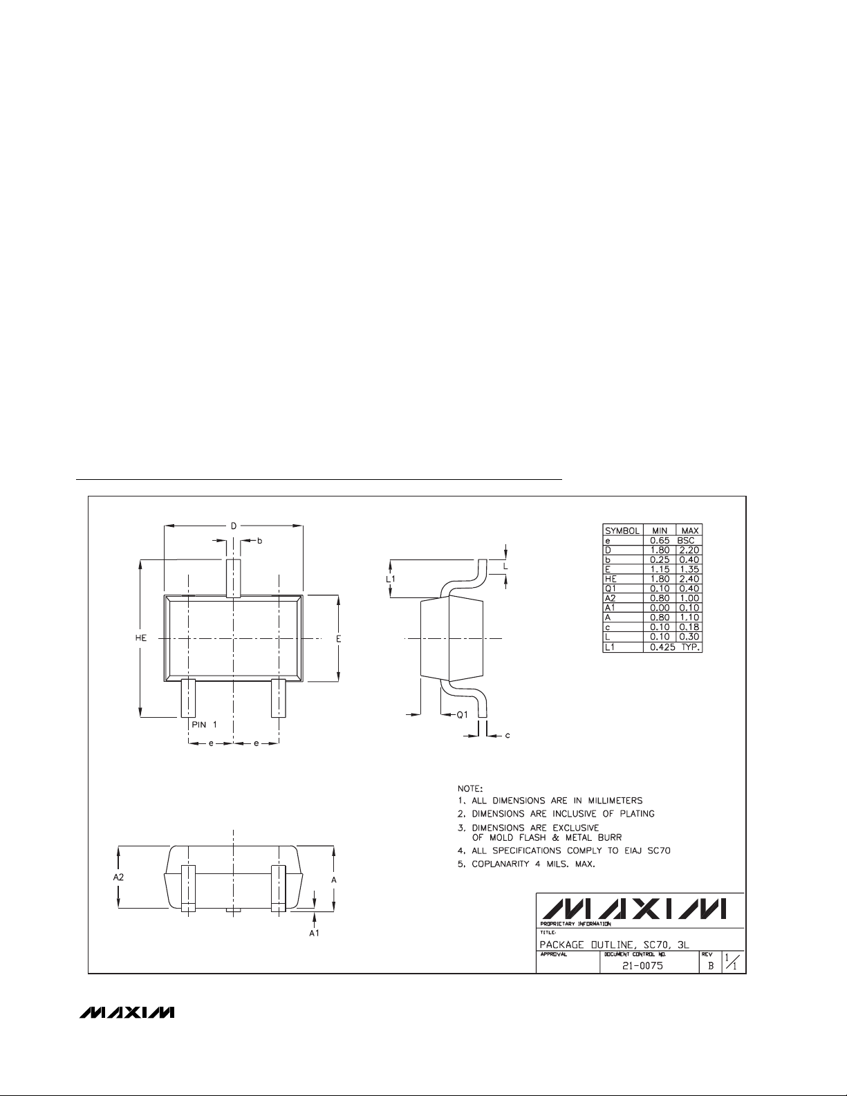
Package Information
SC70, 3L.EPS
Page 8
MAX803L/M/R/S/T/Z, MAX809J/L/M/R/S/T/Z, MAX810L/M/R/S/T/Z
3-Pin Microprocessor Reset Circuits
Maxim cannot assume responsibility for use of any circuitry other than circuitry entirely embodied in a Maxim product. No circuit patent licenses are
implied. Maxim reserves the right to change the circuitry and specifications without notice at any time.
8 _____________________Maxim Integrated Products, 120 San Gabriel Drive, Sunnyvale, CA 94086 408-737-7600
© 2001 Maxim Integrated Products Printed USA is a registered trademark of Maxim Integrated Products.
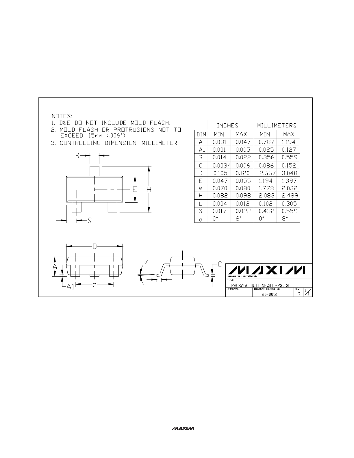
Package Information (continued)
SOTPO3L.EPS
 Loading...