

Page 1
19-1175; Rev 0; 12/96
with Synchronous Rectifier for CPU Power
High-Accuracy Step-Down Controller
_______________General Description
The MAX798†high-performance, step-down DC-DC
converter provides main CPU power in battery-powered
systems. This buck controller achieves 96% efficiency
by using synchronous rectification and Maxim’s proprietary Idle Mode™ control scheme to extend battery life
at full-load (up to 10A) and no-load outputs. The
MAX798’s high accuracy meets the demanding requirements of the latest-generation CPUs. Excellent dynamic
response corrects output transients caused by the latest
dynamic-clock CPUs within five 300kHz clock cycles.
Unique bootstrap circuitry drives inexpensive N-channel
MOSFETs, reducing system cost and eliminating the crowbar switching currents found in some PMOS/NMOS switch
designs.
The MAX798 has a logic-controlled and synchronizable
fixed-frequency pulse-width-modulating (PWM) operating
mode, which reduces noise and RF interference in sensitive mobile-communications and pen-entry applications.
The SKIP override input allows automatic switchover to
idle-mode operation (for high-efficiency pulse skipping) at
light loads, or forces fixed-frequency mode for lowest noise
at all loads.
________________________Applications
____________________________Features
♦ 96% Efficiency
♦ 4.5V to 30V Input Range
♦ 1.6V to 6V Adjustable Precision Output
♦ ±0.4% Max Total Load-Regulation Error
♦ 0.06%/V Max Line-Regulation Error
♦ 5V Linear-Regulator Output
♦ Precision 2.505V Reference Output
♦ Automatic Bootstrap Circuit
♦ 150kHz/300kHz Fixed-Frequency PWM Operation
♦ Programmable Soft-Start
♦ 1.2mA Typical Quiescent Current
(VIN= 12V, V
OUT
= 2.5V)
♦ 1µA Typical Shutdown Current
______________Ordering Information
PIN-PACKAGETEMP. RANGEPART
16 Narrow SO-40°C to +85°CMAX798ESE
MAX798
Notebook and Subnotebook Computers
PDAs and Mobile Communicators
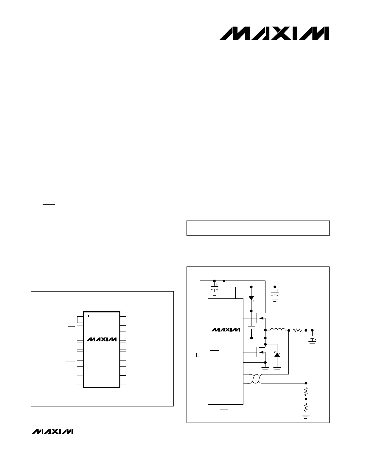
__________________Pin Configuration
TOP VIEW
SS
1
2
SKIP
REF
3
GND
SYNC
SHDN
FB
CSH
Idle Mode is a trademark of Maxim Integrated Products.
†
U.S. and foreign patents pending.
MAX798
4
5
6
7
8
SO
DH
16
LX
15
BST
14
DL
13
PGND
12
VL
11
V+
10
9
CSL
__________Typical Operating Circuit
INPUT
4.5V TO 30V
5V, 25mA
4.7µF
V+ VL
BST
DH
MAX798
ON
OFF
SHDN
GND
LX
DL
PGND
CSH
CSL
FB
0.1µF
N
R
SENSE
N
V
OUT
________________________________________________________________
Maxim Integrated Products
1
For free samples & the latest literature: http://www.maxim-ic.com, or phone 1-800-998-8800
Page 2
High-Accuracy Step-Down Controller
with Synchronous Rectifier for CPU Power
ABSOLUTE MAXIMUM RATINGS
V+ to GND.................................................................-0.3V, +36V
GND to PGND........................................................................±2V
VL to GND ...................................................................-0.3V, +7V
BST to GND...............................................................-0.3V, +36V
DH to LX........................................................-0.3V, (BST + 0.3V)
LX to BST.....................................................................-7V, +0.3V
SHDN to GND............................................................-0.3V, +36V
MAX798
SYNC, SS, REF, SKIP, DL to GND...................-0.3V, (VL + 0.3V)
CSH, CSL to GND .......................................................-0.3V, +7V
VL Short Circuit to GND..............................................Momentary
Stresses beyond those listed under “Absolute Maximum Ratings” may cause permanent damage to the device. These are stress ratings only, and functional
operation of the device at these or any other conditions beyond those indicated in the operational sections of the specifications is not implied. Exposure to
absolute maximum rating conditions for extended periods may affect device reliability.
ELECTRICAL CHARACTERISTICS
(V+ = +15V, GND = PGND = 0V, IVL= I
STEP-DOWN CONTROLLER
Nominal Adjustable Output
Voltage Range
Current-Limit Voltage
INTERNAL REGULATOR AND REFERENCE
= 0A, TA= 0°C to +85°C, unless otherwise noted.)
REF
CONDITIONS
External resistor divider
CSH - CSL = 40mV, SKIP = VL
0mV < (CSH - CSL) < 80mV, SKIP = VL
6V < V+ < 30V
CSH - CSL, positive
CSH - CSL, negative
SHDN = 2V, 0mA <IVL< 25mA, 5.5V < V+ < 30V
Rising edge, hysteresis = 15mV
Rising edge, hysteresis = 25mV
No external load (Note 1) V2.463 2.505 2.537Reference Output Voltage
Falling edge V1.8 2.3Reference Fault Lockout Voltage
0µA < I
SHDN = 0V, CSL = 6V, V+ = 0V or 30V, VL = 0V
SHDN = 0V, V+ = 30V, CSL = 0V or 6V
FB = CSH = CSL = 6V, VL switched over to CSL µA15V+ Off-State Leakage Current
V+ = 4V, CSL = 0V (Note 2) mW6.6 10.5Dropout Power Consumption
CSH = CSL = 6V mW6.4 8.5Quiescent Power Consumption
REF
< 100µA mV20Reference Load Regulation
REF Short Circuit to GND...........................................Continuous
VL Output Current...............................................................50mA
Continuous Power Dissipation (T
SO (derate 8.70mW/°C above +70°C)........................696mW
Operating Temperature Range
MAX798ESE....................................................-40°C to +85°C
Storage Temperature Range.............................-65°C to +160°C
Lead Temperature (soldering, 10sec).............................+300°C
= +70°C)
A
80 100 120
-40 -100 -160
UNITSMIN TYP MAXPARAMETER
V4.5 30Input Supply Range
V1.6 6
V1.576 1.6 1.624Feedback Voltage
%±0.4Load Regulation
%/V0.04 0.05Line Regulation
mV
µA2.0 4.0 6.5SS Source Current
mA2.0SS Fault Sink Current
V4.75 5.25VL Output Voltage
V3.8 4.0VL Fault Lockout Voltage
V4.2 4.7VL/CSL Switchover Voltage
µA0.1 1CSL Shutdown Leakage Current
µA15V+ Shutdown Current
2 _______________________________________________________________________________________
Page 3
High-Accuracy Step-Down Controller
with Synchronous Rectifier for CPU Power
ELECTRICAL CHARACTERISTICS (continued)
(V+ = +15V, GND = PGND = 0V, IVL= I
Oscillator Frequency
Maximum Duty Cycle
Input High Voltage
Input Low Voltage
Input Current
= 0A, TA= 0°C to +85°C, unless otherwise noted.)
REF
CONDITIONS UNITSMIN TYP MAXPARAMETER
SYNC = REF
SYNC = 0V or 5V
Guaranteed by design
SYNC = REF
SYNC = 0V or 5V
SYNC
SHDN, SKIP
SYNC
SHDN, SKIP
SHDN, 0V or 30V
SYNC, SKIP
CSH, CSL, CSH = CSL = 4V, device not shut down
FB, FB = 1.6V ±100 nA
DL forced to 2V
DH forced to 2V, BST - LX = 4.5V A1DH Sink/Source Current
High or low
High or low, BST - LX = 4.5V
270 300 330
125 150 175
89 91
93 96
VL - 0.5
2.0
0.8
0.5
2
1
50
kHz
ns200SYNC High Pulse Width
ns200SYNC Low Pulse Width
ns200SYNC Rise/Fall Time
kHz195 340Oscillator Sync Range
%
V
V
µA
µA
A1DL Sink/Source Current
Ω7DL On-Resistance
Ω7DH On-Resistance
MAX798
_______________________________________________________________________________________ 3
Page 4
High-Accuracy Step-Down Controller
with Synchronous Rectifier for CPU Power
ELECTRICAL CHARACTERISTICS
(V+ = +15V, GND = PGND = 0V, IVL= I
STEP-DOWN CONTROLLER
Nominal Adjustable Output
MAX798
Voltage Range
Current-Limit Voltage
INTERNAL REGULATOR AND REFERENCE
OSCILLATOR AND INPUTS/OUTPUTS
Oscillator Frequency
Maximum Duty Cycle
= 0A, TA= -40°C to +85°C, unless otherwise noted.) (Note 3)
REF
CONDITIONS UNITSMIN TYP MAXPARAMETER
External resistor divider V1.6 6.0
CSH - CSL = 40mV, SKIP = VL
0mV < (CSH - CSL) < 80mV, SKIP = VL
6V < V+ < 30V %/ V0.04 0.06Line Regulation
CSH - CSL, positive
CSH - CSL, negative -40 -100 -160
SHDN = 2V, 0mA < IVL< 25mA, 5.5V < V+ < 30V
Rising edge, hysteresis = 15mV
Rising edge, hysteresis = 25mV
No external load (Note 1)
0µA < I
SHDN = 0V, V+ = 30V, CSL = 0V or 6V
FB = CSH = CSL = 6V, VL switched over to CSL
CSH = CSL = 6V
SYNC = REF
SYNC = 0V or 5V
SYNC = REF
SYNC = 0V or 5V
High or low
High or low, BST - LX = 4.5V
REF
< 100µA
70 130
4.15 4.75VL/CSL Switchover Voltage
250 300 350
110 150 190
250SYNC Low Pulse Width
88 91
92 96
V5.0 30Input Supply Range
V1.560 1.6 1.640Feedback Voltage
%±1Load Regulation
mV
V4.7 5.3VL Output Voltage
V3.75 4.05VL Fault Lockout Voltage
V
V2.438 2.505 2.562Reference Output Voltage
mV30Reference Load Regulation
µA110V+ Shutdown Current
µA110V+ Off-State Leakage Current
mW6.4 9.1Quiescent Power Consumption
kHz
ns250SYNC High Pulse Width
ns
kHz210 320Oscillator Sync Range
%
Ω7DL On-Resistance
Ω7DH On-Resistance
Note 1: Since the reference uses VL as its supply, V+ line-regulation error is insignificant.
Note 2: At very low input voltages, quiescent supply current can increase due to excess PNP base current in the VL linear
regulator. This occurs only if V+ falls below the preset VL regulation point (5V nominal). The typical maximum quiescent
current in dropout will not exceed 16mA.
Note 3: All -40°C to +85°C specifications above are guaranteed by design.
4 _______________________________________________________________________________________
Page 5

High-Accuracy Step-Down Controller
SKIP
with Synchronous Rectifier for CPU Power
______________________________________________________________Pin Description
PIN
10 V+
11 VL
12 PGND Power Ground
NAME FUNCTION
1 SS Soft-Start Timing Capacitor Connection. Ramp time to full current limit is approximately 1ms/nF.
Disables pulse-skipping mode when high. Connect to GND for normal use. Don’t leave
2
3 REF Reference Voltage Output. Bypass to GND with 0.33µF minimum.
4 GND Low-Noise Analog Ground and Feedback Reference Point
5 SYNC
6
7 FB Feedback Input. Regulates at FB = 1.6V. Connect FB to a resistor divider to set the output voltage.
8 CSH Current-Sense Input, high side. Current-limit level is 100mV referred to CSL.
9 CSL Current-Sense Input, low side
SKIP
SHDN
With SKIP grounded, the device will
tion when the load current exceeds approximately 30% of maximum.
Oscillator Synchronization and Frequency Select. Tie to GND or VL for 150kHz operation; tie to REF for
300kHz operation. A high-to-low transition begins a new cycle. Drive SYNC with 0V to 5V logic levels (see the
Electrical Characteristics
Shutdown Control Input, active low. Logic threshold is set at approximately 1V (VTHof an internal N-channel
MOSFET). Tie SHDN to V+ for automatic start-up.
Battery Voltage Input (4.5V to 30V). Bypass V+ to PGND close to the IC with a 0.1µF capacitor. Connects to a
linear regulator that powers VL.
5V Internal Linear-Regulator Output. VL is also the supply voltage rail for the chip. VL is switched to the output voltage via CSL (V
up to 5mA for external loads.
table for VIHand VILspecifications). SYNC capture range is 195kHz to 340kHz.
> 4.5V) for automatic bootstrapping. Bypass to GND with 4.7µF. VL can supply
CSL
automatically
change from pulse-skipping operation to full PWM opera-
unconnected.
MAX798
13 DL Low-Side Gate-Drive Output. Normally drives the synchronous-rectifier MOSFET. Swings 0V to VL.
14 BST Boost Capacitor Connection for high-side gate drive (0.1µF)
15 LX Switching Node (inductor) Connection. Can swing 2V below ground without hazard.
16 DH
High-Side Gate-Drive Output. Normally drives the main buck switch. DH is a floating driver output that swings
from LX to BST, riding on the LX switching-node voltage.
_______________________________________________________________________________________ 5
Page 6

High-Accuracy Step-Down Controller
with Synchronous Rectifier for CPU Power
, 4.5V TO 30V
V
IN
R3
2.2µF
10Ω
4.7µF
MAX798
ON
SKIP
0.33µF
OFF
V+
REF
SHDN
MAX798
0.01µF
SS
SYNC
Q1, Q2 =
SILICONIX Si4410DY or IRF7413
C1, C2 =
10µF/30V SANYO OS-CON (30SA10)
C4 =
470µF/4V SPRAGUE 594D SERIES (594D477X0004R2T)
L1 =
SUMIDA CDRH127 120
R1 =
6.49kΩ, 1%
R2 =
11.5kΩ, 1%
f =
150kHz
VL
BST
DH
PGND
CSH
CSL
GND
LX
DL
FB
R4
1M
C3
47pF
0.1µF
C1
C2
Q1
L1
12µH
Q2
15mΩ
470pF
, +2.5V @ 4.2A
V
OUT
C4
C5
R1
R2
Figure 1. Standard Application Circuit
_______________Detailed Description
The MAX798 is a BiCMOS, switch-mode power-supply
controller designed primarily for buck-topology regulators in battery-powered applications where high accuracy, high efficiency, and low quiescent supply current
are critical. The MAX798 also works well in other
topologies such as boost, inverting, and CUK due to
the flexibility of its floating high-speed gate driver.
Light-load efficiency is enhanced by automatic idlemode operation—a variable-frequency pulse-skipping
mode that reduces losses due to MOSFET gate charge.
The step-down power-switching circuit consists of two
N-channel MOSFETs, a rectifier, and an LC output filter.
The output voltage is the average of the AC voltage at
the switching node, which is adjusted and regulated by
changing the duty cycle of the MOSFET switches. The
gate-drive signal to the N-channel high-side MOSFET
must exceed the battery voltage and is provided by a
flying capacitor boost circuit that uses a 100nF capacitor connected between BST and LX.
6 _______________________________________________________________________________________
Page 7

High-Accuracy Step-Down Controller
with Synchronous Rectifier for CPU Power
The MAX798 contains the following seven major circuit
blocks, which are shown in Figure 2.
PWM Controller Blocks:
• Multi-Input PWM Comparator
• Current-Sense Circuit
• PWM Logic Block
• Gate-Driver Outputs
BATTERY VOLTAGE
V+
+5V LINEAR
REGULATOR
SHDN
SKIP
TO
CSL
4.5V
PWM
LOGIC
Bias Generator Blocks:
• +5V Linear Regulator
• Automatic Bootstrap Switchover Circuit
• +2.505V Reference
OUT
VL
BST
DH
LX
+5V AT 5mA
MAIN
OUTPUT
MAX798
+2.505V
REF
+2.505V
AT 100µA
ON/OFF
REF
GND
SHDN
SS
Figure 2. Functional Diagram
_______________________________________________________________________________________
1.6V
PWM
COMPARATOR
MAX798
DL
PGND
CSH
1X
CSL
FB
SYNC
7
Page 8

High-Accuracy Step-Down Controller
with Synchronous Rectifier for CPU Power
These internal IC blocks aren’t powered directly from
the battery. Instead, a +5V linear regulator steps down
the battery voltage to supply both the IC internal rail (VL
pin) as well as the gate drivers. The synchronousswitch gate driver is directly powered from +5V VL,
while the high-side-switch gate driver is indirectly powered from VL via an external diode-capacitor boost circuit. An automatic bootstrap circuit turns off the +5V
MAX798
linear regulator and powers the IC from its output voltage if the output is above 4.5V.
PWM Controller Block
The heart of the current-mode PWM controller is a multiinput open-loop comparator that sums three
signals: output voltage error signal with respect to the
reference voltage, current-sense signal, and slope
compensation ramp (Figure 3). The PWM controller is
a direct summing type, lacking a traditional error
amplifier and the phase shift associated with it. This
direct-summing configuration approaches the ideal of
cycle-by-cycle control over the output voltage.
For more comprehensive information on the MAX798
internal blocks, please refer to the MAX796/MAX797/
MAX799 data sheet.
__________Applications Information
Powering VL from a +5V Supply
If the circuit’s output voltage is greater than the VL/CSL
switchover voltage, the IC automatically bootstraps and
runs off its output. Running from the high-efficiency output rather than the VL linear regulator is particularly
desirable if the input voltage is high. If the output is
not greater than the VL/CSL switchover threshold,
efficiency can be improved by powering VL from
another efficient system supply (Figure 4).
VL can be connected directly to a +5V supply, provided its maximum excursions are within a 4.5V to 6V
range and the main output voltage’s maximum is less
than 4.2V. If the circuit’s output voltage is greater than
4.2V, the IC can activate its internal bootstrap switch
and connect the circuit output to VL.
Adjusting the Output Voltage
The output voltage is set by an external resistor divider
between the output voltage and GND, with the midpoint
connected to FB (Figure 5). The output voltage can be
adjusted from 1.6V to 6V, according to the formula in
Figure 5. Recommended R2 values range from 5kΩ to
100kΩ. For best noise immunity, place R1 and R2 close
to FB. For a 1.6V output, connect the output voltage
directly to FB.
Remote sensing of the output voltage is easily achieved
by connecting the top of R1 and, if desired, the bottom
of R2, to the remote sense point.
Bypassing and
Compensation Components
The MAX798 is designed to deliver a more accurate
output voltage than the MAX797. A major source of the
MAX797’s output error is the decrease in output voltage
with increasing load. This error is greatly reduced in the
MAX798 by increasing the gain of the voltage-sense
signal relative to the current-sense signal. As a result of
this increased gain, the MAX798 is slightly more noise
sensitive than the MAX797, and requires some small
compensation components as well. On the other hand,
output capacitor ESR requirements can be greatly
relaxed compared to the MAX797, with the limiting factor being the maximum total output voltage ripple that
the application can tolerate.
To control noise problems, place the bypass capacitors
on REF, VL, and V+ as close as possible to the IC, and
use a 10Ω series resistor (R3, Figure 1) on V+ to form a
small lowpass filter. Feed-forward components (R4, C3,
and C5) are chosen for stable switching at 150kHz with
the components shown. For 300kHz switching and a
4.7µH inductor, use R4 = 470kΩ and C5 = 220pF.
Keep the components that connect to FB (R4, C5, R1,
R2) close to the IC’s FB pin.
Design Procedure
With the exception of the items previously mentioned,
follow the design procedure for the MAX797. The
MAX796/MAX797/MAX799 data sheet contains all necessary information on component values, component
selection, layout, and additional applications.
8 _______________________________________________________________________________________
Page 9

High-Accuracy Step-Down Controller
with Synchronous Rectifier for CPU Power
CSH
1X
1.6V
MAIN PWM
COMPARATOR
CSL
FROM
FEEDBACK
DIVIDER
MAX798
SKIP
SHDN
–100mV
R
Q
S
SLOPE COMP
30mV
VL
4µA
2.5V
24R
1R
SYNCHRONOUS
RECTIFIER CONTROL
SS
N
CURRENT
LIMIT
R
Q
S
OSC
MAX798
LEVEL
SHIFT
SHOOT-
THROUGH
CONTROL
LEVEL
SHIFT
BST
DH
LX
VL
DL
PGND
Figure 3. PWM Controller Detailed Block Diagram
_______________________________________________________________________________________ 9
Page 10

High-Accuracy Step-Down Controller
with Synchronous Rectifier for CPU Power
0.1µF
V
BATT
5V ±10%
MAX798
V+ VL
MAX798
DH
DL
Figure 4. Powering VL from a Separate +5V Supply
(MAX) < 4.2V)
(V
OUT
V+
DH
REMOTE
SENSE
LINES
MAIN
OUTPUT
MAX798
DL
CSH
CSL
FB
V
OUT
GND
= 1.6V
V
OUT
R1
(1 + –––)
R2
R1
R2
Figure 5. Adjusting the Output Voltage
10 ______________________________________________________________________________________
Page 11

High-Accuracy Step-Down Controller
with Synchronous Rectifier for CPU Power
___________________Chip Information
TRANSISTOR COUNT: 1008
________________________________________________________Package Information
DIM
D
A
0.101mm
e
A1
B
0.004in.
C
L
0°-8°
A
A1
B
C
E
e
H
L
INCHES MILLIMETERS
MIN
0.053
0.004
0.014
0.007
0.150
0.228
0.016
MAX
0.069
0.010
0.019
0.010
0.157
0.244
0.050
MIN
1.35
0.10
0.35
0.19
3.80
5.80
0.40
MAX
1.75
0.25
0.49
0.25
4.00
1.270.050
6.20
1.27
MAX798
PINS
Narrow SO
HE
SMALL-OUTLINE
PACKAGE
(0.150 in.)
______________________________________________________________________________________ 11
DIM
D
D
D
INCHES MILLIMETERS
MIN
MAX
8
0.189
0.197
14
0.337
0.344
16
0.386
0.394
MIN
4.80
8.55
9.80
MAX
5.00
8.75
10.00
21-0041A
Page 12

High-Accuracy Step-Down Controller
with Synchronous Rectifier for CPU Power
NOTES
MAX798
Maxim cannot assume responsibility for use of any circuitry other than circuitry entirely embodied in a Maxim product. No circuit patent licenses are
implied. Maxim reserves the right to change the circuitry and specifications without notice at any time.
12
__________________Maxim Integrated Products, 120 San Gabriel Drive, Sunnyvale, CA 94086 (408) 737-7600
© 1996 Maxim Integrated Products Printed USA is a registered trademark of Maxim Integrated Products.
 Loading...