

Page 1
19-0201; Rev 0; 11/93
Evaluation Kit
Available
12V/15V or Adjustable, High-Efficiency,
Low IQ, Step-Up DC-DC Converters
_______________General Description
The MAX761/MAX762 step-up switching regulators
provide high efficiency over a wide range of load currents,
delivering up to 150mA. A unique, current-limited
pulse-frequency-modulated (PFM) control scheme gives
the devices the benefits of pulse-width-modulated (PWM)
converters (high efficiency with heavy loads), while using
less than 110µA of supply current (vs. 2mA to 10mA for
PWM converters). The result is high efficiency over a wide
range of loads.
The MAX761/MAX762 input voltage range is 2V to 16.5V.
Output voltages are preset to 12V (MAX761) and 15V
(MAX762), or they can be set with two external resistors.
With a 5V input, the MAX761 guarantees a 12V, 150mA
output. Its high efficiency, low supply current, fast start-up
time, SHDN controlling capability, and small size make the
MAX761 ideal for powering flash memory.
The MAX761/MAX762 have an internal 1A power MOSFET, making them ideal for minimum-component, low- and
medium-power applications. These devices use tiny external components, and their high switching frequencies (up
to 300kHz) allow for small surface-mount magnetics.
For increased output drive capability or higher output voltages, use the MAX770–MAX773, which are similar in
design to the MAX761/MAX762, but drive external power
MOSFETs. For stepping up to 5V, see the MAX756/
MAX757 and MAX856-MAX859 data sheets.
_________________________Applications
Flash Memory Programming
PCMCIA Cards
Battery-Powered Applications
High-Efficiency DC-DC Converters
____________________________Features
♦ High Efficiency for a Wide Range of Load Currents
♦ 12V/150mA Flash Memory Programming Supply
♦ 110µA Max Supply Current
♦ 5µA Max Shutdown Supply Current
♦ 2V to 16.5V Input Voltage Range
♦ 12V (MAX761), 15V (MAX762) or Adjustable Output
♦ Current-Limited PFM Control Scheme
♦ 300kHz Switching Frequency
♦ Internal, 1A, N-Channel Power FET
♦ LBI/LBO Low-Battery Comparator
______________Ordering Information
PART TEMP. RANGE PIN-PACKAGE
MAX761CPA
MAX761CSA 0°C to +70°C 8 SO
MAX761C/D 0°C to +70°C Dice*
MAX761EPA -40°C to +85°C 8 Plastic DIP
MAX761ESA -40°C to +85°C 8 SO
MAX761MJA -55°C to +125°C 8 CERDIP**
MAX762CPA
MAX762CSA 0°C to +70°C 8 SO
MAX762C/D 0°C to +70°C Dice*
MAX762EPA -40°C to +85°C 8 Plastic DIP
MAX762ESA -40°C to +85°C 8 SO
MAX762MJA -55°C to +125°C 8 CERDIP**
* Contact factory for dice specifications.
** Contact factory for availability and processing to MIL-STD-883.
0°C to +70°C 8 Plastic DIP
0°C to +70°C 8 Plastic DIP
MAX761/MAX762
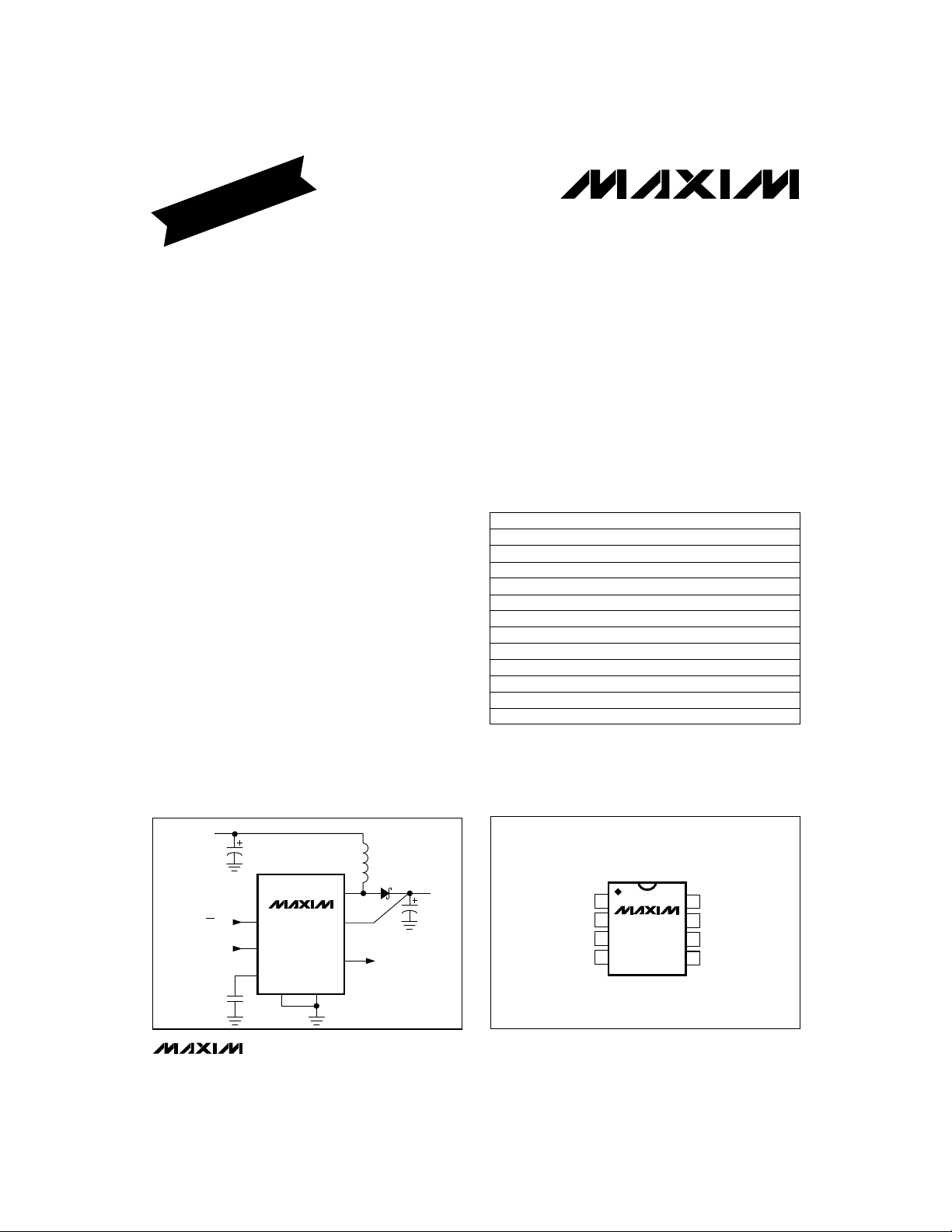
__________Typical Operating Circuit
INPUT
4.75V
TO 12V
DETECTOR INPUT
ON/OFF
LOW-BATTERY
33µF
MAX761
SHDN
LBI
REF
FB
GND
________________________________________________________________
LBO
18µH
OUTPUT
12V
LX
V+
150mA
33µF
LOW-BATTERY
DETECTOR OUTPUT
__________________Pin Configuration
TOP VIEW
LBO
1
2
LBI
MAX761
MAX762
3
FB
4
SHDN
DIP/SO
Maxim Integrated Products
Call toll free 1-800-998-8800 for free samples or literature.
V+
8
LX
7
GND
6
REF
5
1
Page 2
12V/15V or Adjustable, High-Efficiency,
Low IQ, Step-Up DC-DC Converters
ABSOLUTE MAXIMUM RATINGS
Supply Voltage V+ to GND.......................................-0.3V to 17V
REF, LBO, LBI, SHDN, FB............................-0.3V to (V+ + 0.3V)
LX..............................................................................-0.3V to 17V
LX Peak Current....................................................................1.5A
LBO Current..........................................................................5mA
Continuous Power Dissipation (T
Plastic DIP (derate 9.09mW/°C above +70°C) ............727mW
SO (derate 5.88mW/°C above +70°C).........................471mW
CERDIP (derate 8.00mW/°C above +70°C).................640mW
Stresses beyond those listed under “Absolute Maximum Ratings” may cause permanent damage to the device. These are stress ratings only, and functional
operation of the device at these or any other conditions beyond those indicated in the operational sections of the specifications is not implied. Exposure to
absolute maximum rating conditions for extended periods may affect device reliability.
ELECTRICAL CHARACTERISTICS
MAX761/MAX762
(V+ = 5V, I
Minimum Operating Voltage 1.7 V
Minimum Start-Up Voltage 1.7 2.0 V
Supply Current
Shutdown Current 15µA
Output Voltage
(Note 1)
Peak Current at LX I
Maximum Switch-On Time t
Minimum Switch-Off Time t
Load Regulation 0.0042 %/mA
Line Regulation 0.08 %/V
Efficiency 86 %
Reference Voltage V
= 0mA, C
LOAD
PARAMETER SYMBOL MIN TYP MAX
= +70°C)
A
= 0.1µF, TA= T
REF
V
OUT
PEAK
ON
OFF
REF
to T
MIN
Figure 2, bootstrapped
Figure 3 or 5 with
external resistors.
Figure 2, bootstrapped
Figure 2, bootstrapped
V+ = 16.5V, normal operation, SHDN = 0V,
non-bootstrapped
Figure 2, MAX761, VIN= 5V, SHDN = 0V,
normal operation
V+ = 10.0V, shutdown mode, SHDN = V+
Figure 2,
MAX761,
bootstrapped
Figure 2,
MAX762,
bootstrapped
See Figure 4b
Figure 2, 0mA ≤ I
Figure 2, 4V ≤ VIN≤ 6V, bootstrapped
Figure 2, bootstrapped, V
60mA ≤ I
MAX76_C
MAX76_E
MAX76_M
typical values are at TA= +25°C, unless otherwise noted.)
MAX,
LOAD
Operating Temperature Ranges:
MAX76_C_A........................................................0°C to +70°C
MAX76_E_A.....................................................-40°C to +85°C
MAX76_MJA ..................................................-55°C to +125°C
Junction Temperatures:
MAX76_C_A/E_A..........................................................+150°C
MAX76_MJA.................................................................+175°C
Storage Temperature Range.............................-65°C to +160°C
Lead Temperature (soldering, 10sec).............................+300°C
CONDITIONS
2 16.5
MAX76_C/E
MAX76_M
0mA ≤ I
3V ≤ V+ ≤ 12V
0mA ≤ I
4.75V ≤ V+ ≤ 12V
0mA ≤ I
3V ≤ V+ ≤ 15V
0mA ≤ I
4.75V ≤ V+ ≤ 15V
≤ 200mA, bootstrapped
LOAD
≤ 120mA
OUT
LOAD
LOAD
LOAD
LOAD
= 12V,
≤ 75mA,
≤ 150mA,
≤ 50mA,
≤ 100mA,
3 16.5Supply Voltage V+
3.1 16.5
88 110
300
11.52 12.0 12.48
11.52 12.0 12.48
14.4 15.0 15.6
14.4 15.0 15.6
0.75 1.0 1.25 A
6810µs
1.0 1.3 1.6 µs
1.4700 1.50 1.5300
1.4625 1.50 1.5375
1.4550 1.50 1.5450
UNITS
V
µA
V
V
2 _______________________________________________________________________________________
Page 3
12V/15V or Adjustable, High-Efficiency,
Low IQ, Step-Up DC-DC Converters
ELECTRICAL CHARACTERISTICS (continued)
(V+ = 5V, I
Reference Load Regulation
Reference Line Regulation
LX Leakage Current
Voltage Trip Point
LX On Resistance
SHDN Input High Voltage
SHDN Input Low Voltage V
SHDN Leakage Current -1 1 µA
LBI Threshold Voltage
LBI Hysteresis 20 mV
LBI Leakage Current
LBO Leakage Current -1 1 µA
LBO Voltage V
LBI to LBO Delay 2.5 µs
= 0mA, C
LOAD
PARAMETER
= 0.1µF, TA= T
REF
SYMBOL MIN TYP MAX
FB
V
FB
V
IH
IL
OL
to T
MIN
0µA ≤ I
3.0V ≤ V+ ≤ 16.5V
V+ = 16.5V,
LX = 17V
MAX76_C
MAX76_E
MAX76_M
MAX76_C
MAX76_E
MAX76_M
V+ > 5.0V
2.0V ≤ V+ ≤ 16.5V
2.0V ≤ V+ ≤ 16.5V
V+ = 16.5V, SHDN = 0V or V+
LBI falling
V+ = 16.5V, V
V+ = 16.5V, V
V+ = 5.0V, I
Overdrive = 5mV
, typical values are at TA= +25°C, unless otherwise noted.)
MAX
CONDITIONS
≤ 100µA
LOAD
= 1.5V
LBI
= 16.5V
LBO
= 1mA
SINK
MAX76_C/E
MAX76_M
MAX76_C
MAX76_E
MAX76_M
MAX76_C
MAX76_E
MAX76_M
-5 5
-10 10
-30 30
-20 20
-40 40FB Leakage Current I
-60 60
1.4700 1.50 1.5300
1.4625 1.50 1.5375
1.4550 1.50 1.5450
1.6 V
1.4700 1.50 1.5300
1.4625 1.50 1.5375
1.4550 1.50 1.5450
-20 20 nA
10
15
30 100 µV/V
1.0 2.2
0.4 V
0.4 V
MAX761/MAX762
UNITS
mV
µA
nA
V
Ω
V
Note 1: See
to switching on and off times, on-resistance, and peak-current ratings.
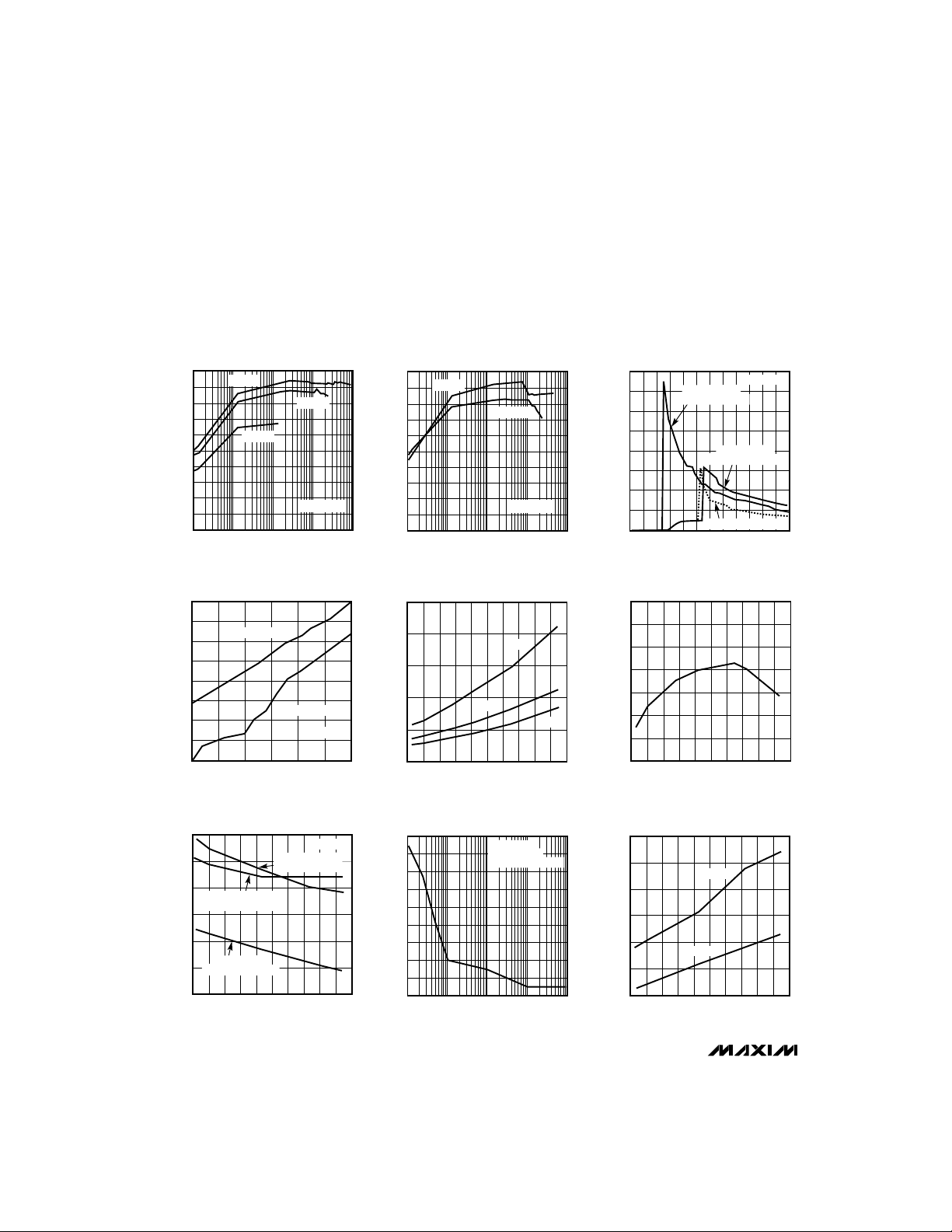
Typical Operating Characteristics
_______________________________________________________________________________________ 3
for output current capability versus input voltage. Guarantees based on correlation
Page 4
12V/15V or Adjustable, High-Efficiency,
Low IQ, Step-Up DC-DC Converters
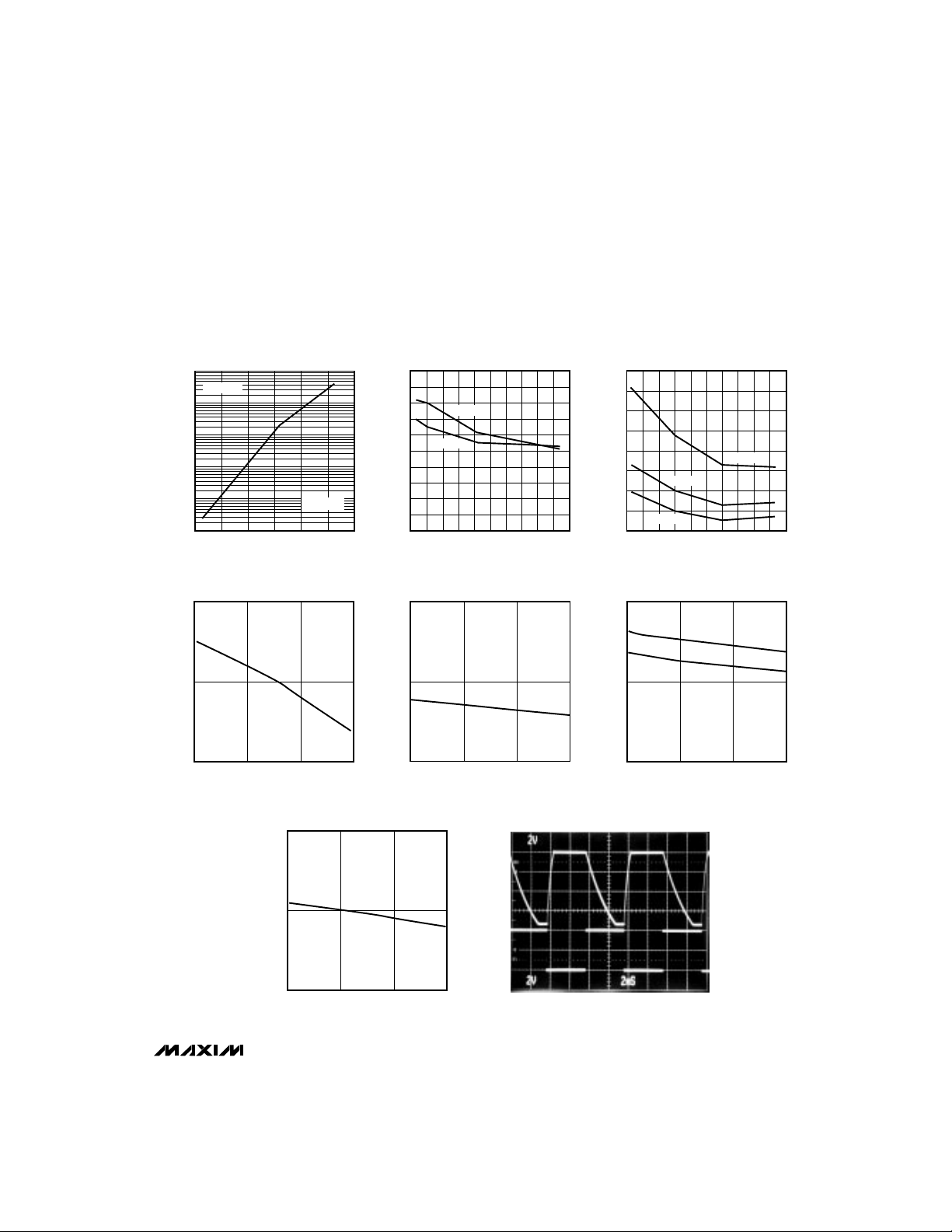
__________________________________________Typical Operating Characteristics
(Circuit of Figure 2, TA= +25°C, unless otherwise noted.)
EFFICIENCY vs. OUTPUT CURRENT
100
90
80
70
60
50
40
EFFICIENCY (%)
30
20
MAX761/MAX762
10
0
0.1 10 1000
400
350
300
250
200
150
100
MAXIMUM OUTPUT CURRENT (mA)
50
0
3.0 6.0
BOOTSTRAPPED
VIN = 10V
VIN = 5V
VIN = 2V
V
= 12V
OUT
1 100
OUTPUT CURRENT (mA)
MAXIMUM OUTPUT CURRENT vs.
INPUT VOLTAGE
BOOTSTRAPPED
NON-BOOTSTRAPPED
V
= 12V
OUT
4.0
3.5 4.5 5.5
SUPPLY VOLTAGE (V)
5.0
NO-LOAD START-UP VOLTAGE
3.5
3.0
2.5
NON-BOOTSTRAPPED
(EXTERNAL RESISTORS)
2.0
1.5
BOOTSTRAPPED
1.0
(INTERNAL RESISTORS)
NO-LOAD START-UP VOLTAGE (V)
0.5
-60 -20 60 140
-40 0 8040 120
20 100
TEMPERATURE (°C)
V
= 12V
OUT
BOOTSTRAPPED
(EXTERNAL RESISTORS)
EFFICIENCY vs. OUTPUT CURRENT
100
90
MAX761-01
80
70
60
50
40
EFFICIENCY (%)
30
20
10
0
250
MAX761-04
200
150
100
50
REFERENCE OUTPUT RESISTANCE (Ω)
0
2.2
MAX761-07
2.1
2.0
1.9
1.8
1.7
1.6
START-UP VOLTAGE (V)
1.5
1.4
1.3
NON-BOOTSTRAPPED
VIN = 10V
0.1 10 1000
1 100
OUTPUT CURRENT (mA)
REFERENCE OUTPUT RESISTANCE vs.
TEMPERATURE
-60 -20 60 140
-40 0 8040 120
0.1 10 1000
20 100
TEMPERATURE (°C)
MAX761
START-UP VOLTAGE vs. R
1 100
R
LOAD
VIN = 5V
V
= 12V
OUT
10µA
50µA
LOAD
V
= 12V
OUT
BOOTSTRAPPED
INTERNAL RESISTORS
(kΩ)
100µA
2.00
MAX761-02
1.75
1.50
1.25
1.00
0.75
0.50
QUIESCENT CURRENT (mA)
0.25
0
01 3 6
1.506
MAX761-05
1.504
1.502
1.500
1.498
1.496
REFERENCE OUTPUT (V)
1.494
1.492
-60 -20 60 140
1.6
MAX761-08
1.4
1.2
1.0
0.8
LX ON-RESISTANCE (Ω)
0.6
0.4
-60 -20 60 140
QUIESCENT CURRENT vs.
INPUT VOLTAGE
V
= 12V
BOOTSTRAPPED
(INTERNAL RESISTORS)
24
0.5 1.5 3.52.5 4.5 5.5
INPUT VOLTAGE (V)
REFERENCE vs.TEMPERATURE
COEFFICIENT
20 100-40 0 8040 120
TEMPERATURE (°C)
LX ON-RESISTANCE vs.
TEMPERATURE
V+ = 5V
V+ = 12V
-40 0 8040 120
20 100
TEMPERATURE (°C)
OUT
BOOTSTRAPPED
(EXTERNAL RESISTORS)
NON-BOOTSTRAPPED
5
MAX761-03
MAX761-06
MAX761-09
4 _______________________________________________________________________________________
Page 5
12V/15V or Adjustable, High-Efficiency,
Low IQ, Step-Up DC-DC Converters
____________________________Typical Operating Characteristics (continued)
(Circuit of Figure 2, TA= +25°C, unless otherwise noted.)
LX LEAKAGE vs. TEMPERATURE
1000
V+ = 15V
100
10
1
LX LEAKAGE (nA)
0.1
0.01
20 120
TEMPERATURE (°C)
SWITCH-ON TIME vs. TEMPERATURE
8.5
(µs)
8.0
on
t
VLX = 16.5V
V+ = 5V
PEAK CURRENT AT LX vs. TEMPERATURE
MAX761-11
(µA)
CC
I
4.0
3.5
3.0
2.5
2.0
1.5
1.0
0.5
0
1.5
1.4
MAX761-10
1.3
1.2
1.1
(A)
1.0
PEAK
I
0.9
0.8
0.7
0.6
0.5
1401008040 60
-60 -20 60 140
V+ = 12V
V+ = 5V
20 100-40 0 8040 120
TEMPERATURE (°C)
SWITCH-OFF TIME vs. TEMPERATURE
MAX761-13
(µs)
off
t
2.0
V+ = 5V
1.5
MAX761-14
(µA)
CC
I
100
90
SHUTDOWN CURRENT
vs. TEMPERATURE
V+ = 15V
V+ = 8V
V+ = 4V
-60 -20 60 140
20 100-40 0 8040 120
TEMPERATURE (°C)
POWER-SUPPLY CURRENT
vs. TEMPERATURE
V+ = 16.5V
V+ = 3V
MAX761/MAX762
MAX761-12
MAX761-15
7.5
-60 60
0 120
TEMPERATURE (°C)
RATIO (µs/µs)
off
/t
on
t
_______________________________________________________________________________________
1.0
SWITCH-ON/SWITCH-OFF TIME RATIO
7
6
5
-60 60
vs.TEMPERATURE
V+ = 5V
0 120
TEMPERATURE (°C)
-60 60
0 120
TEMPERATURE (°C)
MAX761-16
I
= 100mA, VIN = 5V
LOAD
A: V
, 2V/div
OUT
B: SHDN (0V to 4V)
80
-60 60
SHDN RESPONSE TIME
2ms/div
0 120
TEMPERATURE (°C)
12V
5V
4V
0V
5
Page 6

12V/15V or Adjustable, High-Efficiency,
Low IQ, Step-Up DC-DC Converters
_____________________________Typical Operating Characteristics (continued)
(Circuit of Figure 2, TA= +25°C, unless otherwise noted.)
LOAD–TRANSIENT RESPONSE
200mA
A
0mA
B
LINE–TRANSIENT RESPONSE
6V
A
4V
B
MAX761/MAX762
5µs/div
A: I
, (0mA to 200mA)
LOAD
B: V
, AC COUPLED, 100mV/div
OUT
VIN = 5V, V
= 12V
OUT
A: VIN (4V to 6V)
B: V
, AC COUPLED, 20mV/div
OUT
I
= 50mA, V
OUT
______________________________________________________________Pin Description
PIN
1
2
3
4
5
6
7
8
NAME FUNCTION
LBO
LBI Input to the internal low-battery comparator. Tie to GND or V+ if not used.
FB
SHDN
REF
GND Ground
LX
V+ Power-supply input. In bootstrapped mode, V+ is also the output voltage sense input.
Low-battery output is an open-drain output that goes low when LBI is less than 1.5V.
Connect to V+ through a pull-up resistor. Leave LBO floating if not used.
Feedback input. For fixed-output bootstrapped operation, connect FB to GND. For
adjustable-output bootstrapped operation, connect a resistor divider between V+, FB and
GND. For non-bootstrapped operation, there is no fixed-output option. Connect a resistor
divider network between V
Modes
section.
Active-high TTL/CMOS logic-level input. In shutdown mode (SHDN = V+), the internal
switch is turned off and the output voltage equals V+ minus a diode drop (due to the DC
path from the input to the output). Tie to GND for normal operation.
1.5V reference output that can source 100µA for external loads. Bypass with 0.1µF
or larger capacitor.
Drain of the internal N-channel FET. LX has an output resistance of 1Ω and a peak current
limit of 1A.
, FB and GND. See
OUT
5ms/div
= 12V
OUT
Bootstrapped/Non-Bootstrapped
6 _______________________________________________________________________________________
Page 7

12V/15V or Adjustable, High-Efficiency,
Low IQ, Step-Up DC-DC Converters
LBO V+ FB
MAX761/MAX762
LBI
N
LBI
REF
1.5V
REFERENCE
Q
TRIG
ONE-SHOT
R
CIRCUITRY
Q
CURRENT
COMPARATOR
LOW INPUT
VOLTAGE
OSCILLATOR
TRIG
ONE-SHOT
S
Q
CURRENT CONTROL
Figure 1. Simple Block Diagram
________________Detailed Description
The MAX761/MAX762 BiCMOS step-up switch-mode
power supplies provide fixed outputs of 12V and 15V,
respectively. They have a unique control scheme that
combines the advantages of pulse-frequency modulation
(low supply current) and pulse-width modulation (high
efficiency at high loads). The internal N-channel power
MOSFET allows 1A peak currents, increasing the output
current capability over previous pulse-frequency-modulation (PFM) devices. Figure 1 shows the MAX761/
MAX762 block diagram.
The MAX761/MAX762 offer three main improvements
over prior solutions: (1) the converters operate with tiny
surface-mount inductors (less than 5mm diameter)
Operating Principle
100mV
GND
DUAL-MODE
COMPARATOR
ERROR
COMPARATOR
0.1V0.2V
UNDER VOLTAGE
COMPARATOR
MAX761
MAX762
N
2.5V
N
because of their 300kHz switching frequency, (2) the
current-limited PFM control scheme allows 86% efficiencies over a wide range of load currents, and (3) the maximum supply current is only 110µA.
Bootstrapped/Non-Bootstrapped Modes
Figures 2 and 3 show the standard application circuits
for bootstrapped and non-bootstrapped modes. In bootstrapped mode, the IC is powered from the output
(V
). In other words, the current needed to power the
OUT
bootstrapped circuit is different from the V+ current the
chip consumes. The voltage applied to the gate of the
internal N-channel FET is switched from V
OUT
providing more switch-gate drive and increasing the efficiency of the DC-DC converter compared with non-bootstrapped operation.
V+
LX
to ground,
_______________________________________________________________________________________ 7
Page 8

12V/15V or Adjustable, High-Efficiency,
Low IQ, Step-Up DC-DC Converters
V
+5V
R4
R3
=
IN
C1
33µF
C3
0.1µF
L1
18µH
5
REF
MAX761
4
SHDN
2
LBI
3
FB
MAX761/MAX762
LX
GND
D1
1N5817
7
8
V+
1
LBO
6
+12V at
150mA
C2
0.1µF
LOW-BATTERY
OUTPUT
Figure 2. Bootstrapped Operating Circuit
In non-bootstrapped mode, the IC is powered from the
supply voltage, VIN, and operates with minimum supply
current. Since the voltage applied to the gate of the internal FET is reduced, efficiency declines with low input
voltages. Note: In non-bootstrapped mode, there is no
fixed-output operation; external resistors must be
used to set the output voltage. Use 1% external feed-
back resistors when operating in non-bootstrapped
mode (Figure 3).
Use bootstrapped mode when VINis below approximately 4V. For VINbetween 4V and 6V, the trade-off is
lower supply current in non-bootstrapped mode versus
higher output current in bootstrapped mode (see
Typical Operating Characteristics
).
Pulse-Frequency Modulation
(PFM) Control Scheme
The MAX761/MAX762 use a proprietary current-limited
PFM control scheme. This control scheme combines
the ultra-low supply current of pulse-skipping PFM converters with the high full-load efficiency characteristic of
current-mode pulse-width-modulation (PWM) converters. It allows the devices to achieve high efficiency over
a wide range of loads, while the current-sense function
and high operating frequency allow the use of tiny
external components.
As with traditional PFM converters, the internal power
MOSFET is turned on when the voltage comparator
senses the output is out of regulation (Figure 1).
However, unlike traditional PFM converters, switching is
accomplished through the combination of a peak cur-
C4
33µF
100k
V
IN
R4
R3
LOW-BATTERY
DETECT
V
( )
R4 = R3
V
= 1.5V NOMINAL
REF
C1 = 33µF
C2 = 0.1µF
C3 = 0.1µF
C4 = 33µF
C1
TRIP
L1
18µH
8
V+
C2
2
LBI
5
REF
C3
4
SHDN
- V
REF
V
REF
LX
MAX761
MAX762
GND
D1
1N5817
7
7
6
C4
FB
LBO
ADJUSTABLE
OUTPUT (V
R2 = R1 ( -1)
R2
3
R1
1
LOW-BATTERY
DETECT OUTPUT
OUT
V
V
100k
)
OUT
REF
Figure 3. Non-Bootstrapped Operating Circuit
rent limit and a pair of one-shots that set the maximum
on-time (8µs) and minimum off-time (1.3µs) for the
switch. Once off, the minimum off-time one-shot holds
the switch off for 1.3µs. After this minimum time, the
switch either (1) stays off if the output is in regulation, or
(2) turns on again if the output is out of regulation.
The MAX761/MAX762 also limit the peak inductor current, allowing the devices to run in continuous-conduction mode (CCM) and maintain high efficiency with
heavy loads (Figure 4a). This current-limiting feature is
a key component of the control circuitry. Once turned
on, the switch stays on until either (1) the maximum ontime one-shot turns it off (8µs later), or (2) the current
limit is reached.
To increase light-load efficiency, the current limit for the
first two pulses is set to half the peak current limit. If
those pulses bring the output voltage into regulation,
the voltage comparator holds the MOSFET off, and the
current limit remains at half the peak current limit. If the
output voltage is still out of regulation after two pulses,
the current limit for the next pulse is raised to the full
current limit of 1A (Figure 4b).
Internal vs. External Resistors
When external feedback resistors are used, an internal
undervoltage lockout system prevents start-up until V+
rises to about 2.7V. When external feedback resistors are
8 _______________________________________________________________________________________
Page 9

12V/15V or Adjustable, High-Efficiency,
Low IQ, Step-Up DC-DC Converters
MAX761/MAX762
, LBO (an
REF
1A
500mA
0A
1A
500mA
Figure 4a. CCM, Heavy Load Current Waveform (500mA/div) Figure 4b. Light/Medium Load Current Waveform (500mA/div)
used in a bootstrapped circuit (Figure 5), undervoltage
lockout prevents start-up at low input voltages; but
once started, operation can continue down to a lower
voltage that depends on the load.
There is no undervoltage lockout when the internal feedback resistors are used (Figure 2), and special circuitry
guarantees start-up at 2.0V. The start-up circuitry fixes
the duty cycle at 50% until V+ is driven to 2.5V, above
which the normal control system takes over.
Shutdown Mode
The MAX761/MAX762 enter shutdown mode when
SHDN is high. In this mode, the internal biasing circuitry
is turned off (including the reference) and V
V+ minus a diode drop (due to the DC path from the
input to the output). In shutdown mode, the supply current drops to less than 5µA. SHDN is a TTL/CMOS logic
level input. Connect SHDN to GND for normal operation.
LBO is high impedance during shutdown.
OUT
equals
Modes of Operation
When delivering high output currents, the MAX761/
MAX762 operate in CCM. In this mode, current always
flows in the inductor, and the control circuit adjusts the
switch’s duty cycle on a cycle-by-cycle basis to maintain
regulation without exceeding the switch-current capability. This provides excellent load-transient response and
high efficiency.
In discontinuous-conduction mode (DCM), current
through the inductor starts at zero, rises to a peak value,
then ramps down to zero on each cycle. Although efficiency is still excellent, the switch waveforms contain
ringing (the inductor's self-resonant frequency). This
ringing is normal and poses no operational problems.
Low-Battery Detector
The MAX761/MAX762 provide a low-battery comparator
that compares the voltage on LBI to the 1.5V reference
voltage. When the LBI voltage is below V
open-drain output) goes low. The low-battery comparator’s 20mV of hysteresis adds noise immunity, preventing repeated triggering of LBO. Use a resistor-divider
network between V+, LBI, and GND to set the desired
trip voltage V
ignored and LBO is high impedance. The value of
resistor R3 should be no larger than 500kΩ to ensure
the LBI leakage current does not cause inaccuracies in
V
.
TRIP
(Figure 3). When SHDN is high, LBI is
TRIP
__________________Design Procedure
The MAX761/MAX762’s output voltage can be adjusted
from 5V to 16.5V using external resistors R1 and R2
configured as shown in Figures 3 and 5. For adjustableoutput operation, select feedback resistor R1 in the
10kΩ to 250kΩ range. Higher R1 values within this
range give lowest supply current and best light-load
efficiency. R2 is given by:
R2 = (R1)(
where V
Note: Tie FB to GND for fixed-output operation
(bootstrapped mode only).
REF
= 1.5V.
Setting the Output Voltage
V
OUT
- 1)
V
REF
_______________________________________________________________________________________ 9
Page 10

12V/15V or Adjustable, High-Efficiency,
Low IQ, Step-Up DC-DC Converters
LX
GND
D1
1N5817
7
8
V+
R2
3
FB
R1
6
R2 = R1
( -1)
L1
V
IN
C1 = 33µF
MAX761/MAX762
C2 = 0.1µF
C3 = 0.1µF
C4 = 33µF
Figure 5. Bootstrapped Operation with Adjustable Output
18µH
C1
MAX761
5
REF
2
LBI
4
SHDN
MAX762
V
= 1.5V NOMINAL
REF
C3
Selecting the Inductor (L)
In both CCM and DCM, practical inductor values range
from 10µH to 50µH. If the inductor value is too low, the
current in the coil will ramp up to a high level before the
current-limit comparator can turn off the switch. The minimum on-time for the switch (t
) is approximately
ON(min)
2.5µs, so select an inductance that allows the current to
ramp up to I
of I
/2allows the half-size pulses to occur, giving high-
LIM
/2in no less than 2.5µs. Choosing a value
LIM
er light-load efficiency and minimizing ripple. Hence, calculate the minimum inductance value as:
where V
(V
L ≥
OR
L ≥ (V
is in volts and L is in microhenries.
IN(max)
IN(max)
IN(max)
I
LIM
)(t
ON(min)
/2
)(5)
)
The coil’s inductance need not satisfy this criterion
exactly, as the circuit can tolerate a wide range of values. Larger inductance values tend to produce physically larger coils and increase the start-up time, but are otherwise acceptable. Smaller inductance values allow the
coil current to ramp up to higher levels before the switch
can turn off, producing higher ripple at light loads. In
general, an 18µH inductor is sufficient for most applications (VIN≤ 5V). An 18µH inductor is appropriate for
input voltages up to 3.6V, as calculated above. However,
the same 18µH coil can be used with input voltages up
to 5V with only small increases in peak current, as shown
in Figures 4a and 4b.
Inductors with a ferrite core or equivalent are recom-
V
OUT
mended. The inductor’s incremental saturation-current
rating should be greater than the 1A peak current limit. It
is generally acceptable to bias the inductor into satura-
C4
tion by approximately 20% (the point where the inductance is 20% below the nominal value). For highest efficiency, use a coil with low DC resistance, preferably
under 100mΩ. To minimize radiated noise, use a toroid,
C2
a pot core, or a shielded coil.
Table 1 lists inductor types and suppliers for various
applications. The listed surface-mount inductors’ efficiencies are nearly equivalent to those of the larger throughhole inductors.
Diode Selection
The MAX761/MAX762’s high switching frequency
demands a high-speed rectifier. Use a Schottky diode
V
OUT
V
REF
with a 1A average current rating, such as a 1N5817. For
high-temperature applications, use a high-speed silicon
diode, such as the MUR105 or the EC11FS1. These
diodes have lower high-temperature leakage than
Schottky diodes (Table 1).
Capacitor Selection
Output Filter Capacitor
The primary criterion for selecting the output filter capacitor (C4) is low effective series resistance (ESR). The
product of the inductor current variation and the output
filter capacitor’s ESR determines the amplitude of the
high-frequency ripple seen on the output voltage. A
33µF, 16V Sanyo OS-CON capacitor with 100mΩ ESR
typically provides 100mV ripple when stepping up from
5V to 12V at 150mA.
Because the output filter capacitor’s ESR affects efficiency, use low-ESR capacitors for best performance. The
smallest low-ESR SMT tantalum capacitors currently
available are the Sprague 595D series. Sanyo OS-CON
organic semiconductor through-hole capacitors and
Nichicon PL series also exhibit very low ESR. Table 1
lists some suppliers of low-ESR capacitors.
Input Bypass Capacitors
The input bypass capacitor, C1, reduces peak currents
drawn from the voltage source, and also reduces noise
at the voltage source caused by the MAX761/MAX762’s
switching action. The input voltage source impedance
determines the size of the capacitor required at the V+
input. As with the output filter capacitor, a low-ESR
capacitor is recommended. For output currents up to
250mA, 33µF (C1) is adequate, although smaller bypass
capacitors may also be acceptable. Bypass the IC separately with a 0.1µF ceramic capacitor, C2, placed close
to the V+ and GND pins.
10 ______________________________________________________________________________________
Page 11

12V/15V or Adjustable, High-Efficiency,
Low IQ, Step-Up DC-DC Converters
Bypass REF with a 0.1µF capacitor. REF can source up
Reference Capacitor
to 100µA.
Setting the Low-Battery Detector Voltage
To set the low-battery detector’s falling trip voltage
(V
), select R3 between 10kΩ and 500kΩ (Figures 2
TRIP
and 3), and calculate R4 as follows:
(V
- V
R4 = R3 [
TRIP
)
REF
REF
]
V
where VREF = 1.5V.
The rising trip voltage is higher because of the compara-
tor’s hysteresis of approximately 20mV, and can be calculated by:
V
(rising) = (V
TRIP
+ 20mV)(1 + R4/R3).
REF
Connect a high-value resistor (larger than R3 + R4)
between LBI and LBO if additional hysteresis is required.
Table 1. Component Suppliers
PRODUCTION METHOD
Surface Mount
Miniature Through-Hole
Low-Cost Through-Hole
INDUCTORS DIODES
Sumida
CD54-180 (22µH)
Coiltronics
CTX 100-series
Sumida
RCH855-180M
Renco
RL 1284-18
Matsuo
267 series
Sanyo
OS-CON series
Low-ESR organic
semiconductor
Nichicon
PL series
Low-ESR electrolytics
United Chemi-Con
LXF series
Connect a pull-up resistor (e.g., 100kΩ) between LBO
and V
. Tie LBI to GND or V+ and leave LBO floating
OUT
if the low-battery detector is not used.
___________Applications Information
Proper PC board layout is essential because of high current levels and fast switching waveforms that radiate
noise. Minimize ground noise by connecting GND, the
input bypass-capacitor ground lead, and the output filtercapacitor ground lead to a single point (star ground configuration). Also minimize lead lengths to reduce stray
capacitance, trace resistance, and radiated noise. The
traces connected to FB and LX, in particular, must be
short. Place bypass capacitor C2 as close as possible to
V+ and GND.
CAPACITORS
Layout Considerations
Nihon
EC10 series
Motorola
1N5817,
MUR105
MAX761/MAX762
Coiltronics (USA) (407) 241-7876 FAX (407) 241-9339
Matsuo (USA) (714) 969-2491 FAX (714) 960-6492
Matsuo (Japan) 81-6-337-6450 FAX 81-6-337-6456
Nichicon (USA) (708) 843-7500 FAX (708) 843-2798
Nihon (USA) (805) 867-2555 FAX (805) 867-2556
Renco (USA) (516) 586-5566 FAX (516) 586-5562
Sanyo (USA) (619) 661-6835 FAX (619) 661-1055
Sanyo (Japan) (0720) 70-1005 FAX (0720) 70-1174
Sumida (USA) (708) 956-0666
Sumida (Japan) 81-3-607-5111 FAX 81-3-607-5144
United Chem-Con (USA) (714) 255-9500 FAX (714) 255-9400
______________________________________________________________________________________ 11
Page 12

12V/15V or Adjustable, High-Efficiency,
Low IQ, Step-Up DC-DC Converters
___________________Chip Topography
LBI
LBO
FB
V+
MAX761/MAX762
SHDN
TRANSISTOR COUNT: 492;
SUBSTRATE CONNECTED TO V+.
0.080"
(2.030mm)
LX
0.142"
(3.607mm)
GND
REF
Maxim cannot assume responsibility for use of any circuitry other than circuitry entirely embodied in a Maxim product. No circuit patent licenses are
implied. Maxim reserves the right to change the circuitry and specifications without notice at any time.
12
__________________Maxim Integrated Products, 120 San Gabriel Drive, Sunnyvale, CA 94086 (408) 737-7600
© 1993 Maxim Integrated Products Printed USA is a registered trademark of Maxim Integrated Products.
 Loading...