

Page 1
For free samples & the latest literature: http://www.maxim-ic.com, or phone 1-800-998-8800.
For small orders, phone 1-800-835-8769.
General Description
The MAX7401/MAX7405 8th-order, lowpass, Bessel,
switched-capacitor filters (SCFs) operate from a single
+5V (MAX7401) or +3V (MAX7405) supply. These
devices draw only 2mA of supply current and allow corner frequencies from 1Hz to 5kHz, making them ideal
for low-power post-DAC filtering and anti-aliasing applications. They feature a shutdown mode that reduces
supply current to 0.2µA.
Two clocking options are available on these devices:
self-clocking (through the use of an external capacitor)
or external clocking for tighter corner-frequency control.
An offset adjust pin allows for adjustment of the DC output level.
The MAX7401/MAX7405 Bessel filters provide low overshoot and fast settling. Their fixed response simplifies
the design task to selecting a clock frequency.
Applications
ADC Anti-Aliasing CT2 Base Stations
Post-DAC Filtering Speech Processing
Air-Bag Electronics
Features
♦ 8th-Order, Lowpass Bessel Filters
♦ Low Noise and Distortion: -82dB THD + Noise
♦ Clock-Tunable Corner Frequency (1Hz to 5kHz)
♦ 100:1 Clock-to-Corner Ratio
♦ Single-Supply Operation
+5V (MAX7401)
+3V (MAX7405)
♦ Low Power
2mA (Operating Mode)
0.2µA (Shutdown Mode)
♦ Available in 8-Pin SO/DIP Packages
♦ Low Output Offset: ±5mV
MAX7401/MAX7405
8th-Order, Lowpass, Bessel,
Switched-Capacitor Filters
________________________________________________________________
Maxim Integrated Products
1
OS
OUTV
DD
1
2
87CLK
SHDNIN
GND
COM
SO/DIP
TOP VIEW
3
4
6
5
MAX7401
MAX7405
V
DD
IN
CLK
OUT
GND
INPUT
0.1µF
0.1µF
CLOCK
SHDN
OUTPUT
V
SUPPLY
COM
OS
MAX7401
MAX7405
Typical Operating Circuit
19-4788; Rev 1; 6/99
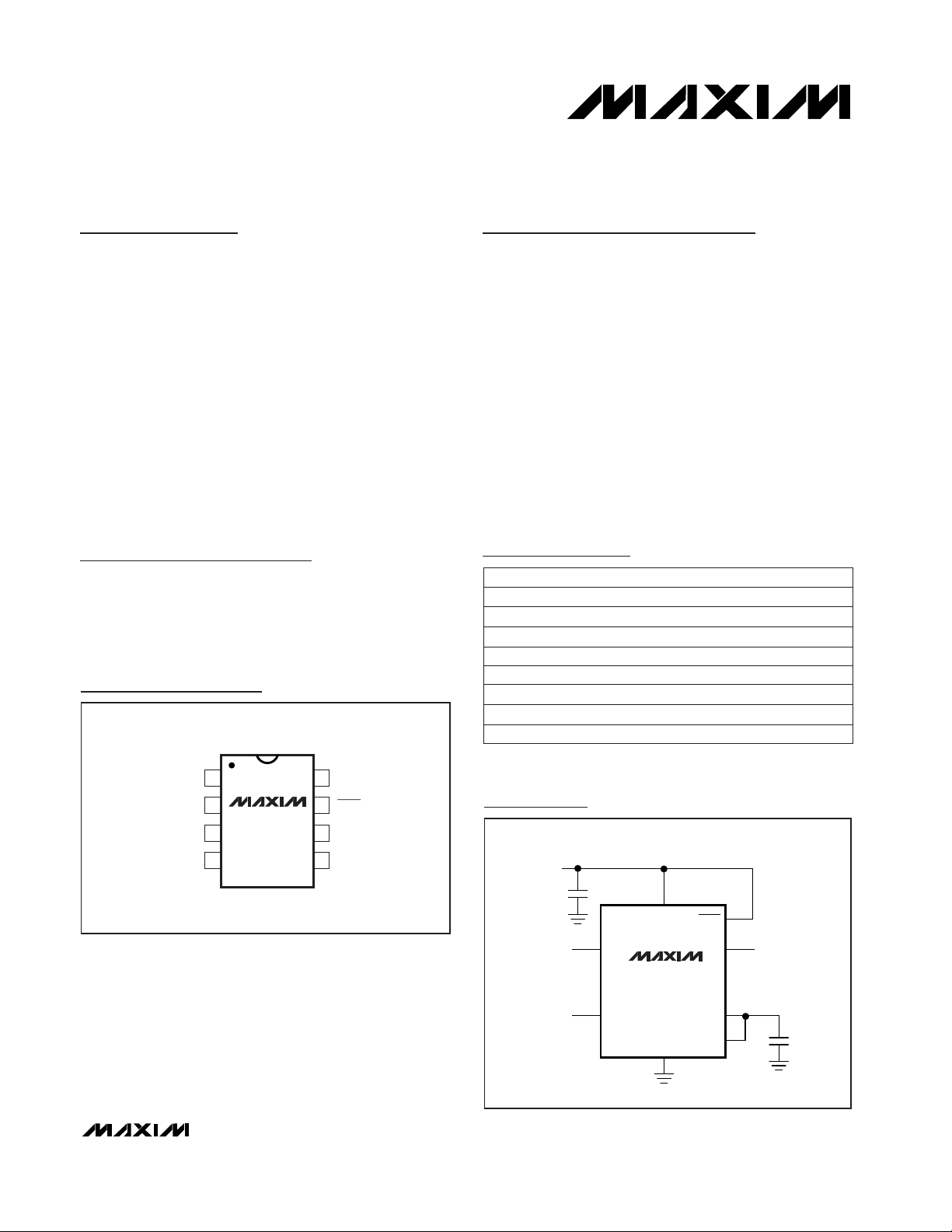
Pin Configuration
Ordering Information
PART
MAX7401CPA
MAX7401ESA
MAX7401EPA -40°C to +85°C
-40°C to +85°C
0°C to +70°C
TEMP. RANGE PIN-PACKAGE
8 Plastic DIP
8 SO
8 Plastic DIP
MAX7405CSA
MAX7405CPA
MAX7405ESA
MAX7405EPA -40°C to +85°C
-40°C to +85°C
0°C to +70°C
0°C to +70°C 8 SO
8 Plastic DIP
8 SO
8 Plastic DIP
MAX7401CSA
0°C to +70°C 8 SO
Page 2
MAX7401/MAX7405
8th-Order, Lowpass, Bessel,
Switched-Capacitor Filters
2 _______________________________________________________________________________________
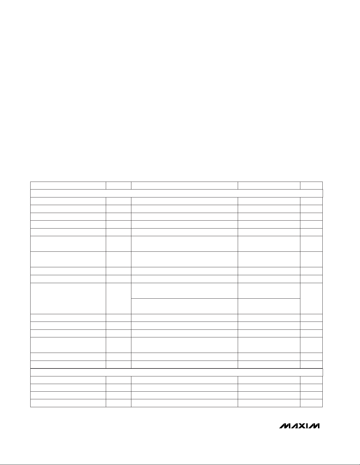
ABSOLUTE MAXIMUM RATINGS
ELECTRICAL CHARACTERISTICS—MAX7401
(VDD= +5V, filter output measured at OUT, 10kΩ || 50pF load to GND at OUT, OS = COM, 0.1µF from COM to GND,
SHDN = VDD, f
CLK
= 100kHz, TA= T
MIN
to T
MAX
, unless otherwise noted. Typical values are at TA= +25°C.)
Stresses beyond those listed under “Absolute Maximum Ratings” may cause permanent damage to the device. These are stress ratings only, and functional
operation of the device at these or any other conditions beyond those indicated in the operational sections of the specifications is not implied. Exposure to
absolute maximum rating conditions for extended periods may affect device reliability.
VDDto GND
MAX7401..............................................................-0.3V to +6V
MAX7405..............................................................-0.3V to +4V
IN, OUT, COM, OS, CLK ...........................-0.3V to (V
DD
+ 0.3V)
SHDN........................................................................-0.3V to +6V
OUT Short-Circuit Duration...................................................1sec
Continuous Power Dissipation (T
A
= +70°C)
8-Pin SO (derate 5.88mW/°C above +70°C)................471mW
8-Pin DIP (derate 9.09mW/°C above +70°C)...............727mW
Operating Temperature Ranges
MAX740 _C_A ....................................................0°C to +70°C
MAX740 _E_A .................................................-40°C to +85°C
Storage Temperature Range.............................-65°C to +150°C
Lead Temperature (soldering, 10sec).............................+300°C
C
OSC
= 1000pF (Note 4)
VOS= 0 to (VDD- 1V) (Note 3)
SHDN = GND, V
COM
= 0 to V
DD
(Note 1)
Input, COM externally driven
fIN= 200Hz, VIN= 4Vp-p,
measurement bandwidth = 22kHz
VIN= V
COM
= V
DD
/ 2
V
COM
= V
DD
/ 2 (Note 2)
CONDITIONS
29 38 48f
OSC
Internal Oscillator Frequency
±0.1 ±10Input Leakage Current at OS
±0.1 ±10Input Leakage Current at COM
50 500C
L
10 1R
L
Resistive Output Load Drive
10Clock Feedthrough
75 125R
COM
Input Resistance at COM
100:1f
CLK
/f
C
Clock-to-Corner Ratio
0.001 to 5f
C
Corner Frequency
V
COM
1A
OS
OS Voltage Gain to OUT
-82THD+N
Total Harmonic Distortion
plus Noise
10Clock-to-Corner Tempco
0.25 V
DD
-
0.25Output Voltage Range
±5 ±25V
OFFSET
Output Offset Voltage
-0.1 0.15 0.3
DC Insertion Gain with
Output Offset Removed
MIN TYP MAX
SYMBOLPARAMETER
V
CLK
= 0 or 5V
0.5V
IL
Clock Input Low
V
DD
- 0.5V
IH
Clock Input High
±15 ±30I
CLK
Clock Input Current
V
V
µA
kHz
µA
µA
pF
kΩ
mVp-p
kΩ
V
V/V
dB
dB
mV
V
ppm/°C
kHz
UNITS
Maximum Capacitive Load at
OUT
COM Voltage Range
V
DD
/ 2
V
DD
/ 2
V
DD
/ 2
- 0.5 + 0.5
V
COM
±0.1V
OS
Input Voltage Range at OS V
V
DD
/ 2
V
DD
/ 2
V
DD
/ 2
- 0.2 + 0.2
FILTER CHARACTERISTICS
CLOCK
Output, COM internally biased
Page 3
MAX7401/MAX7405
8th-Order, Lowpass, Bessel,
Switched-Capacitor Filters
_______________________________________________________________________________________ 3
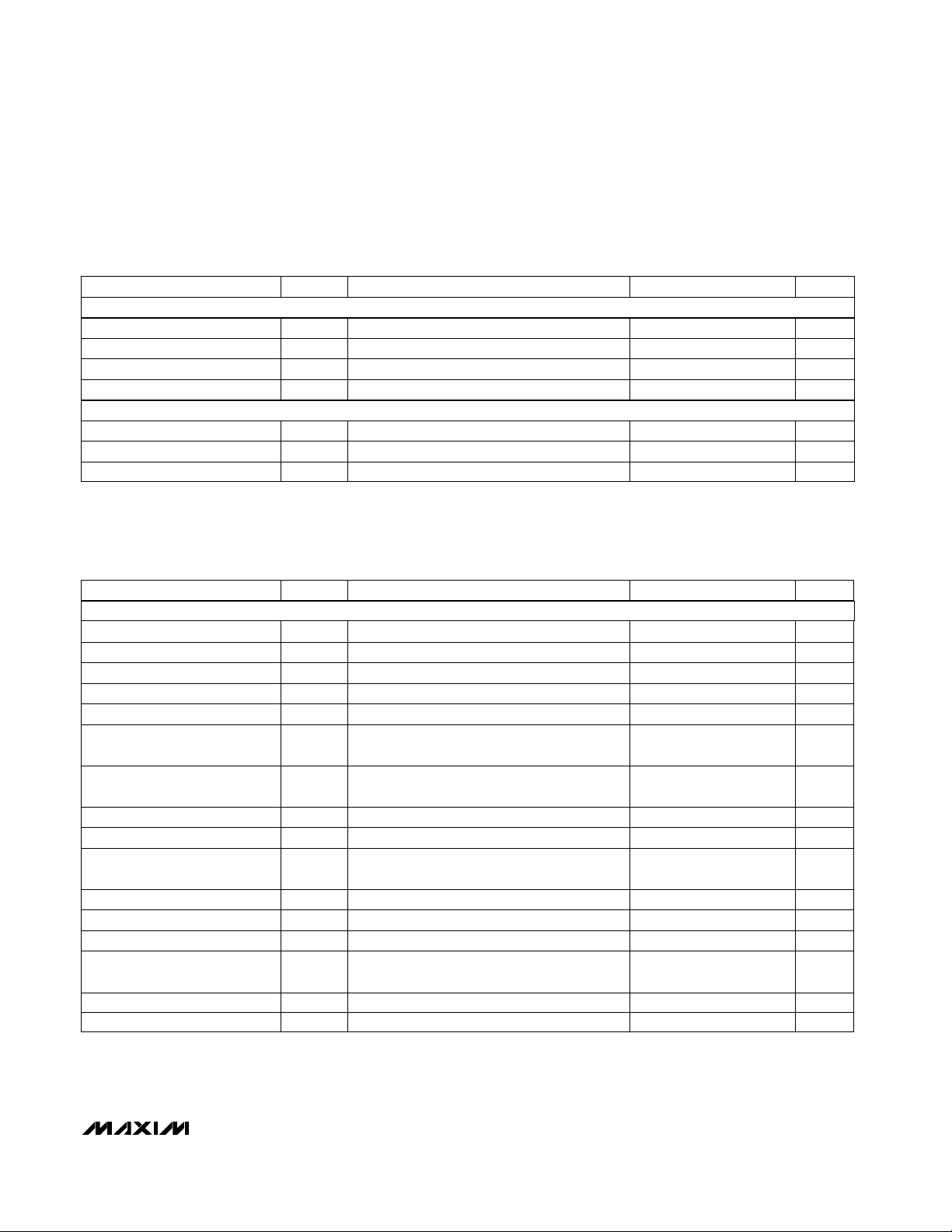
ELECTRICAL CHARACTERISTICS—MAX7401 (continued)
(VDD= +5V, filter output measured at OUT, 10kΩ || 50pF load to GND at OUT, OS = COM, 0.1µF from COM to GND,
SHDN = V
DD
, f
CLK
= 100kHz, TA= T
MIN
to T
MAX
, unless otherwise noted. Typical values are at TA= +25°C.)
ELECTRICAL CHARACTERISTICS—MAX7405
(VDD= +3V, filter output measured at OUT, 10kΩ || 50pF load to GND at OUT, OS = COM, 0.1µF from COM to GND,
SHDN = V
DD
, f
CLK
= 100kHz, TA= T
MIN
to T
MAX
, unless otherwise noted. Typical values are at TA= +25°C.)
CONDITIONS
MIN TYP MAX
SYMBOLPARAMETER
Measured at DC
SHDN = GND, CLK driven from 0 to V
DD
Operating mode, no load, IN = OS = COM
0.5V
SDL
SHDN Input Low
V
DD
- 0.5V
SDH
SHDN Input High
60PSRRPower-Supply Rejection Ratio
0.2 1I
SHDN
Shutdown Current
2 3.5Supply Current I
DD
4.5 5.5V
DD
Supply Voltage
V
V
dB
µA
mA
V
UNITS
SHDN Input Leakage Current V
SHDN
= 0 to V
DD
±0.1 ±10 µA
POWER REQUIREMENTS
SHUTDOWN
µA±0.1 ±10VOS= 0 to (V
DD
- 1V) (Note 3)Input Leakage Current at OS
µA±0.1 ±10
SHDN = GND, V
COM
= 0 to V
DD
Input Leakage Current at COM
Maximum Capacitive
Load at OUT
UNITS
kHz
ppm/°C
V
mV
dB
dB
V/V
V
mVp-p
kΩ
pF
PARAMETER SYMBOL
MIN TYP MAX
DC Insertion Gain with
Output Offset Removed
-0.1 0.03 0.3
Output Offset Voltage V
OFFSET
±5 ±25
Output Voltage Range 0.25 V
DD
-
0.25
Clock-to-Corner Tempco 10
Total Harmonic Distortion
plus Noise
THD+N -84
OS Voltage Gain to OUT A
OS
1
Corner Frequency f
C
0.001 to 5
Clock-to-Corner Ratio f
CLK
/
f
C
100:1
COM Voltage Range V
COM
V
DD
/ 2
V
DD
/ 2
V
DD
/ 2
- 0.1 + 0.1
Clock Feedthrough 10
Resistance Output Load Drive R
L
10 1
C
L
50 500
CONDITIONS
V
COM
= V
DD
/ 2 (Note 2)
VIN= V
COM
= V
DD
/ 2
fIN= 200Hz, VIN= 2.5Vp-p,
measurement bandwidth = 22kHz
(Note 1)
kΩInput Resistance at COM R
COM
75 125
COM internally biased or externally driven
VInput Voltage Range at OS V
OS
V
COM
±0.1
FILTER CHARACTERISTICS
Page 4
MAX7401/MAX7405
8th-Order, Lowpass, Bessel,
Switched-Capacitor Filters
4 _______________________________________________________________________________________
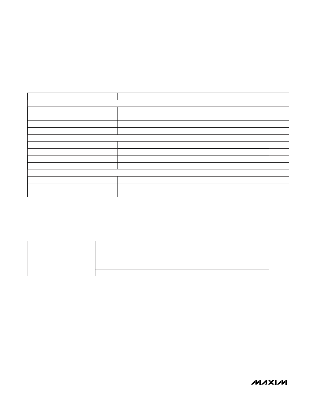
C
OSC
= 1000pF (Note 4)
CONDITIONS
26 34 43f
OSC
Internal Oscillator Frequency
MIN TYP MAX
SYMBOLPARAMETER
Measured at DC
SHDN = GND, CLK driven from 0 to V
DD
Operating mode, no load, IN = OS = COM
V
CLK
= 0 or 3V
0.5V
SDL
SHDN Input Low
V
DD
- 0.5V
SDH
SHDN Input High
60PSRRPower-Supply Rejection Ratio
0.2 1I
SHDN
Shutdown Current
2 3.5
2.7 3.6V
DD
Supply Voltage
0.5V
IL
Clock Input Low
V
DD
- 0.5V
IH
Clock Input High
±15 ±30I
CLK
Clock Input Current
V
V
dB
µA
V
V
V
µA
kHz
UNITS
SHDN Input Leakage Current
V
SHDN
= 0 to V
DD
±0.1 ±10 µA
FILTER CHARACTERISTICS—MAX7401/MAX7405
(VDD= +5V for MAX7401, VDD= +3V for MAX7405; filter output measured at OUT; 10kΩ || 50pF load to GND at OUT; SHDN = VDD;
V
COM = VOS = VDD
/2; f
CLK
= 100kHz; TA = T
MIN
to T
MAX
; unless otherwise noted. Typical values are at TA= +25°C.)
Note 1: The maximum f
C
is defined as the clock frequency, f
CLK
= 100 · fC,at which the peak SINAD drops to 68dB with a sinu-
soidal input at 0.2f
C
.
Note 2: DC insertion gain is defined as ∆V
OUT
/ ∆VIN.
Note 3: OS voltages above V
DD
- 1V saturate the input and result in a 75µA typical input leakage current.
Note 4: For MAX7401, f
OSC
(kHz) ≅ 38 · 103/ C
OSC
(pF). For MAX7405, f
OSC
(kHz) ≅ 34 · 103/ C
OSC
(pF).
CLOCK
POWER REQUIREMENTS
SHUTDOWN
CONDITIONS UNITS
MIN TYP MAX
PARAMETER
mAI
DD
Supply Current
ELECTRICAL CHARACTERISTICS—MAX7405 (continued)
(VDD= +3V, filter output measured at OUT, 10kΩ || 50pF load to GND at OUT, OS = COM, 0.1µF from COM to GND,
SHDN = V
DD
, f
CLK
= 100kHz, TA= T
MIN
to T
MAX
, unless otherwise noted. Typical values are at TA= +25°C.)
fIN= 0.5f
C
-1.0 -0.8 -0.6
fIN= f
C
-3.3 -3.0 -2.7
fIN= 3f
C
-33 -29
fIN= 6f
C
dB
-79 -74
Insertion Gain Relative to
DC Gain
Page 5

MAX7401/MAX7405
8th-Order, Lowpass, Bessel,
Switched-Capacitor Filters
_______________________________________________________________________________________ 5
-70
-50
-60
-40
-10
0
-20
-30
10
012345
FREQUENCY RESPONSE
MAX7401 toc01
INPUT FREQUENCY (kHz)
GAIN (dB)
fC = 1kHz
-3.5
-2.5
-3.0
-2.0
-0.5
0
-1.0
-1.5
0.5
0 202 404 606 808 1010
PASSBAND FREQUENCY RESPONSE
MAX7409 toc02
INPUT FREQUENCY (Hz)
GAIN (dB)
fC = 1kHz
1.97
1.99
1.98
2.01
2.00
2.02
2.03
-40 20 40-20 0 60 80 100
SUPPLY CURRENT
vs. TEMPERATURE
MAX7401 toc05
TEMPERATURE (°C)
SUPPLY CURRENT (mA)
NO LOAD
MAX7401
MAX7405
10,000
0.1
0.01 0.1 1 10 100 1000
INTERNAL OSCILLATOR FREQUENCY
vs. C
OSC
CAPACITANCE
1
MAX7401 toc08
C
OSC
CAPACITANCE (nF)
OSCILLATOR FREQUENCY (kHz)
10
100
1000
-20
-15
-10
-5
0
5
10
15
20
2.5 3.53.0 4.0 4.5 5.0 5.5
OFFSET VOLTAGE
vs. SUPPLY VOLTAGE
MAX7401 toc06
SUPPLY VOLTAGE (V)
OFFSET VOLTAGE (mV)
MAX7401
VIN = V
COM
= V
DD
/ 2
MAX7405
0.80
0.85
0.90
0.95
1.00
1.05
1.10
1.15
1.20
2.5 3.53.0 4.0 4.5 5.0 5.5
NORMALIZED OSCILLATOR FREQUENCY
vs. SUPPLY VOLTAGE
MAX7401 toc09
SUPPLY VOLTAGE (V)
NORMALIZED OSCILLATOR FREQUENCY
C
OSC
= 390pF
MAX7401
MAX7405
-400
-300
-350
-250
-100
-50
-150
-200
0
0 400 800 1200 1600 2000
PHASE RESPONSE
MAX7401 toc03
INPUT FREQUENCY (Hz)
PHASE SHIFT (DEGREES)
fC = 1kHz
1.5
1.8
1.7
1.6
1.9
2.0
2.1
2.2
2.3
2.4
2.5
2.5 3.53.0 4.0 4.5 5.0 5.5
SUPPLY CURRENT
vs. SUPPLY VOLTAGE
MAX7401 toc04
SUPPLY VOLTAGE (V)
SUPPLY CURRENT (mA)
NO LOAD
MAX7405
MAX7401
-1.5
-1.0
0
-0.5
0.5
1.0
-40 0-20 20 40 60 80 100
OFFSET VOLTAGE vs. TEMPERATURE
MAX7401 toc07
TEMPERATURE (°C)
OFFSET VOLTAGE (mV)
VIN = V
COM
= V
DD
/ 2
Typical Operating Characteristics
(VDD= +5V for MAX7401, VDD= +3V for MAX7405; f
CLK
= 100kHz; SHDN = VDD; V
COM
= VOS= VDD/ 2; TA= +25°C; unless otherwise
noted.)
Page 6

MAX7401/MAX7405
8th-Order, Lowpass, Bessel,
Switched-Capacitor Filters
6 _______________________________________________________________________________________
Typical Operating Characteristics (continued)
(VDD= +5V for MAX7401, VDD= +3V for MAX7405; f
CLK
= 100kHz; SHDN = VDD; V
COM
= VOS= VDD/ 2; TA= +25°C; unless otherwise
noted.)
0.96
0.98
0.97
1.00
0.99
1.03
1.02
1.01
1.04
-40 0-20 20 40 60 80 100
NORMALIZED OSCILLATOR FREQUENCY
vs. TEMPERATURE
MAX7401 toc10
TEMPERATURE (°C)
NORMALIZED OSCILLATOR FREQUENCY
C
OSC
= 390pF
MAX7405
MAX7401
-90
-70
-80
-50
-60
-40
-30
-10
-20
0
012
A
B
345
MAX7401
THD PLUS NOISE vs.
INPUT SIGNAL AMPLITUDE
MAX7401 toc11
AMPLITUDE (Vp-p)
THD + NOISE (dB)
NO LOAD
(SEE TABLE A)
-90
-70
-80
-50
-60
-40
-30
-10
-20
0
012345
MAX7401
THD PLUS NOISE vs. INPUT SIGNAL
AMPLITUDE AND RESISTIVE LOAD
MAX7401 toc12
AMPLITUDE (Vp-p)
THD + NOISE (dB)
RL = 500Ω
RL = 1kΩ
RL = 10kΩ
fIN = 200Hz
f
C
= 1kHz
MEASUREMENT BW = 22kHz
TRACE
f
IN
(Hz)
f
C
(kHz)
A 1000 5
B 200 1
f
CLK
(kHz)
500
100
MEASUREMENT
BANDWIDTH (kHz)
80
22
Table A. THD Plus Noise vs. Input
Signal Amplitude Test Conditions
-90
-70
-80
-40
-50
-60
-10
-20
-30
0
0 1.00.5 1.5 2.0 2.5 3.0
MAX7405
THD PLUS NOISE vs.
INPUT SIGNAL AMPLITUDE
MAX7401 toc13
AMPLITUDE (Vp-p)
THD + NOISE (dB)
B
NO LOAD
(SEE TABLE A)
A
-90
-70
-80
-40
-50
-60
-10
-20
-30
0
0 1.00.5 1.5 2.0 2.5 3.0
MAX7405
THD PLUS NOISE vs. INPUT SIGNAL
AMPLITUDE AND RESISTIVE LOAD
MAX7401 toc14
AMPLITUDE (Vp-p)
THD + NOISE (dB)
f
IN
= 200Hz
f
C
= 1kHz
MEASUREMENT BW = 22kHz
R
L
= 500Ω
RL = 1kΩ
RL = 10kΩ
Page 7

MAX7401/MAX7405
8th-Order, Lowpass, Bessel,
Switched-Capacitor Filters
_______________________________________________________________________________________ 7
NAME FUNCTION
1 COM
Common Input. Biased internally at mid-supply. Bypass externally to GND with a 0.1µF capacitor. To override internal biasing, drive with an external supply.
2 IN Filter Input
PIN
3 GND Ground
4 V
DD
Positive Supply Input: +5V for MAX7401, +3V for MAX7405
8 CLK
Clock Input. To override the internal oscillator, connect to an external clock; otherwise, connect an external
capacitor (C
OSC
) from CLK to GND to set the internal oscillator frequency.
7
SHDN
Shutdown Input. Drive low to enable shutdown mode; drive high or connect to VDDfor normal operation.
6 OS
Offset Adjust Input. To adjust output offset, bias OS externally. Connect OS to COM if no offset adjustment is
needed. Refer to
Offset and Common-Mode Input Adjustment
section.
5 OUT Filter Output
Pin Description
_______________Detailed Description
The MAX7401/MAX7405 Bessel filters provide low overshoot and fast settling responses. Both parts operate
with a 100:1 clock-to-corner frequency ratio and a 5kHz
maximum corner frequency.
Lowpass Bessel filters such as the MAX7401/MAX7405
delay all frequency components equally, preserving the
shape of step inputs (subject to the attenuation of the
higher frequencies). Bessel filters settle quickly—an
important characteristic in applications that use a multiplexer (mux) to select an input signal for an analog-todigital converter (ADC). An anti-aliasing filter placed
between the mux and the ADC must settle quickly after
a new channel is selected.
Figure 1 shows the difference between Bessel and
Butterworth filters when a 1kHz square wave is applied
to the filter input. With the filter cutoff frequencies set at
5kHz, trace B shows the Bessel filter response and
trace C shows the Butterworth filter response.
Background Information
Most switched-capacitor filters (SCFs) are designed with
biquadratic sections. Each section implements two filtering poles, and the sections are cascaded to produce
higher order filters. The advantage to this approach is
ease of design. However, this type of design is highly
sensitive to component variations if any section’s Q is
high. An alternative approach is to emulate a passive network using switched-capacitor integrators with summing
and scaling. Figure 2 shows a basic 8th-order ladder filter
structure.
A
2V/div
2V/div
2V/div
C
A: 1kHz INPUT SIGNAL
B: BESSEL FILTER RESPONSE; f
C
= 5kHz
C: BUTTERWORTH FILTER RESPONSE; f
C
= 5kHz
B
200µs/div
Figure 1. Bessel vs. Butterworth Filter Response
L3
L5 L7
C8
R2
C4C2
V
IN
+
-
V
0
L1
R1
C6
Figure 2. 8th-Order Ladder Filter Network
Page 8

MAX7401/MAX7405
8th-Order, Lowpass, Bessel,
Switched-Capacitor Filters
8 _______________________________________________________________________________________
A switched-capacitor filter such as the MAX7401/
MAX7405 emulates a passive ladder filter. The filter’s
component sensitivity is low when compared to a cascaded biquad design because each component affects
the entire filter shape, not just one pole-zero pair. In other
words, a mismatched component in a biquad design will
have a concentrated error on its respective poles, while
the same mismatch in a ladder filter design results in an
error distributed over all poles.
Clock Signal
External Clock
The MAX7401/MAX7405 family of SCFs is designed for
use with external clocks that have a 40% to 60% duty
cycle. When using an external clock with these devices,
drive CLK with a CMOS gate powered from 0 to VDD.
Varying the rate of the external clock adjusts the corner
frequency of the filter as follows:
fC= f
CLK
/ 100
Internal Clock
When using the internal oscillator, connect a capacitor
(C
OSC
) between CLK and ground. The value of the
capacitor determines the oscillator frequency as follows:
where K = 38 for MAX7401 and K = 34 for MAX7405.
Minimize the stray capacitance at CLK so that it does
not affect the internal oscillator frequency. Vary the rate
of the internal oscillator to adjust the filter’s corner frequency by a 100:1 clock-to-corner frequency ratio. For
example, an internal oscillator frequency of 100kHz
produces a nominal corner frequency of 1kHz.
Input Impedance vs. Clock Frequencies
The MAX7401/MAX7405’s input impedance is effectively
that of a switched-capacitor resistor and is inversely proportional to frequency. The input impedance values
determined below represent the average input impedance since the input current is not continuous. As a rule,
use a driver with an output impedance less than 10% of
the filter’s input impedance. Estimate the input impedance of the filter using the following formula:
where f
CLK
= clock frequency and CIN= 3.37pF.
Low-Power Shutdown Mode
These devices feature a shutdown mode that is activated by driving SHDN low. In shutdown mode, the filter’s
supply current reduces to 0.2µA (typ) and its output
becomes high impedance. For normal operation, drive
SHDN high or connect to VDD.
___________Applications Information
Offset and Common-Mode
Input Adjustment
The voltage at COM sets the common-mode input voltage and is biased at mid-supply with an internal resistordivider. Bypass COM with a 0.1µF capacitor and
connect OS to COM. For applications requiring offset
adjustment or DC level shifting, apply an external bias
voltage through a resistor-divider network to OS, as
shown in Figure 3. (Note: Do not leave OS unconnected.) The output voltage is represented by this equation:
V
OUT
= (VIN- V
COM
) + V
OS
with V
COM
= VDD/ 2 (typical), and where (VIN- V
COM
) is
lowpass filtered by the SCF, and VOSis added at the
output stage. See the
Electrical Characteristics
for the
voltage range of COM and OS. Changing the voltage on
COM or OS significantly from mid-supply reduces the filter’s dynamic range.
Power Supplies
The MAX7401 operates from a single +5V supply, and
the MAX7405 operates from a single +3V supply.
Bypass VDDto GND with a 0.1µF capacitor. If dual supplies are required (±2.5V for MAX7401, ±1.5V for
MAX7405), connect COM to system ground and connect
Z
1
f C
IN
CLK IN
=
()
⋅
f (kHz)
K10
C
; C in pF
OSC
3
OSC
OSC
=
⋅
V
DD
V
SUPPLY
IN
CLK
GND
INPUT
OUTPUT
50k
50k
50k
OUT
0.1µF
0.1µF
0.1µF
CLOCK
SHDN
COM
OS
MAX7401
MAX7405
Figure 3. Offset Adjustment Circuit
Page 9

MAX7401/MAX7405
8th-Order, Lowpass, Bessel,
Switched-Capacitor Filters
_______________________________________________________________________________________ 9
GND to the negative supply. Figure 4 shows an example
of dual-supply operation. Single- and dual-supply performance are equivalent. For either single- or dual-supply
operation, drive CLK and SHDN from GND (V- in dualsupply operation) to VDD. For ±5V dual-supply applications, use the MAX291–MAX297.
Input Signal Amplitude Range
The optimal input signal range is determined by observing the voltage level at which the total harmonic distortion plus noise (THD+N) is minimized for a given corner
frequency. The
Typical Operating Characteristics
show
graphs of the devices’ THD+N response as the input
signal’s peak-to-peak amplitude is varied. These measurements are made with OS and COM biased at midsupply.
Anti-Aliasing and Post-DAC Filtering
When using the MAX7401/MAX7405 for anti-aliasing or
post-DAC filtering, synchronize the DAC and the filter
clocks. If the clocks are not synchronized, beat frequencies may alias into the passband.
The high clock-to-corner frequency ratio (100:1) also
eases the requirements of pre- and post-SCF filtering. At
the input, a lowpass filter prevents the aliasing of frequencies around the clock frequency into the passband.
At the output, a lowpass filter attenuates the clock
feedthrough.
A high clock-to-corner frequency ratio allows a simple
RC lowpass filter, with the cutoff frequency set above
the SCF corner frequency, to provide input anti-aliasing
and reasonable output clock attenuation.
Harmonic Distortion
Harmonic distortion arises from nonlinearities within the
filter. These nonlinearities generate harmonics when a
pure sine wave is applied to the filter input. Table 1 lists
the MAX7401/MAX7405’s typical harmonic-distortion
values with a 10kΩ load at TA= +25°C.
V
DD
V+
V-
IN
CLK
GND
INPUT
OUTPUTOUT
0.1µF
CLOCK
*DRIVE SHDN TO V- FOR LOW-POWER SHUTDOWN MODE.
SHDN
COM
OS
0.1µF
MAX7401
MAX7405
*
V+
V-
Figure 4. Dual-Supply Operation
5th
3rd
-92-79
-93-83
500
100
f
CLK
(kHz)
4th
2nd
-92
-90
TYPICAL HARMONIC DISTORTION (dB)
-89
-91
4
5
1
MAX7401
V
IN
(Vp-p)
f
C
(kHz)
FILTER
1000
200
f
IN
(Hz)
Table 1. Typical Harmonic Distortion
TRANSISTOR COUNT: 1116
Chip Information
-88-82
-88-83
500
100
-88
-87
-83
-87
2
5
1
MAX7405
1000
200
Page 10

MAX7401/MAX7405
8th-Order, Lowpass, Bessel,
Switched-Capacitor Filters
10 ______________________________________________________________________________________
________________________________________________________Package Information
SOICN.EPS
Page 11

MAX7401/MAX7405
8th-Order, Lowpass, Bessel,
Switched-Capacitor Filters
______________________________________________________________________________________ 11
Package Information (continued)
PDIPN.EPS
Page 12

MAX7401/MAX7405
8th-Order, Lowpass, Bessel,
Switched-Capacitor Filters
Maxim cannot assume responsibility for use of any circuitry other than circuitry entirely embodied in a Maxim product. No circuit patent licenses are
implied. Maxim reserves the right to change the circuitry and specifications without notice at any time.
12
____________________Maxim Integrated Products, 120 San Gabriel Drive, Sunnyvale, CA 94086 408-737-7600
© 1999 Maxim Integrated Products Printed USA is a registered trademark of Maxim Integrated Products.
NOTES
 Loading...