

Page 1
19-0100; Rev 3; 1/97
EVALUATION KIT MANUALS
FOLLOW DATA SHEET
NiCd/NiMH Battery
Fast-Charge Controllers
_______________General Description
The MAX712/MAX713 fast charge Nickel Metal Hydride
(NiMH) and Nickel Cadmium (NiCd) batteries from a DC
source at least 1.5V higher than the maximum battery
voltage. 1 to 16 series cells can be charged at rates up
to 4C. A voltage-slope detecting analog-to-digital converter, timer, and temperature window comparator determine
charge completion. The MAX712/MAX713 are powered
by the DC source via an on-board +5V shunt regulator.
They draw a maximum of 5µA from the battery when not
charging. A low-side current-sense resistor allows the
battery charge current to be regulated while still
supplying power to the battery’s load.
The MAX712 terminates fast charge by detecting zero
voltage slope, while the MAX713 uses a negative
voltage-slope detection scheme. Both parts come in 16pin DIP and SO packages. An external power PNP transistor, blocking diode, three resistors, and three
capacitors are the only required external components.
For high-power charging requirements, the MAX712/
MAX713 can be configured as a switch-mode battery
charger that minimizes power dissipation. Two evaluation
kits are available: Order the MAX712EVKIT-DIP for quick
evaluation of the linear charger, and the MAX713EVKITSO to evaluate the switch-mode charger.
________________________Applications
Battery-Powered Equipment
Laptop, Notebook, and Palmtop Computers
Handy-Terminals
Cellular Phones
Portable Consumer Products
Portable Stereos
Cordless Phones
____________________________Features
♦ Fast Charge NiMH or NiCd Batteries
♦ Voltage Slope, Temperature, and Timer
Fast-Charge Cutoff
♦ Charge 1 to 16 Series Cells
♦ Supply Battery’s Load while Charging (Linear Mode)
♦ Fast Charge from C/4 to 4C Rate
♦ C/16 Trickle-Charge Rate
♦ Automatically Switch from Fast to Trickle Charge
♦ Linear or Switch-Mode Power Control
♦ 5µA Max Drain on Battery when Not Charging
♦ 5V Shunt Regulator Powers External Logic
______________Ordering Information
PART
MAX712CPE
MAX712CSE
MAX712C/D 0°C to +70°C
MAX712EPE
MAX712ESE
MAX712MJE -55°C to +125°C
Ordering Information continued at end of data sheet.
*
Contact factory for dice specifications.
**
Contact factory for availability and processing to MIL-STD-883.
TEMP. RANGE PIN-PACKAGE
0°C to +70°C
0°C to +70°C
-40°C to +85°C 16 Plastic DIP
-40°C to +85°C
16 Plastic DIP
16 Narrow SO
Dice*
16 Narrow SO
16 CERDIP**
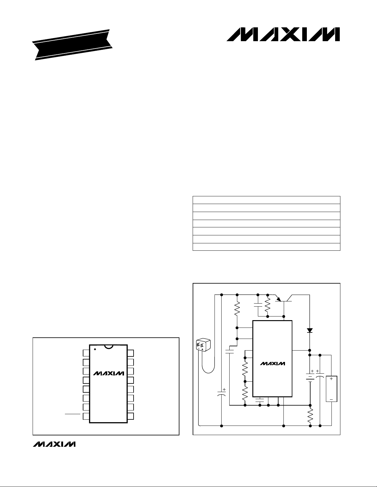
__________Typical Operating Circuit
R2
150Ω
Q1
2N6109
DC IN
R1
C4
0.01µF
MAX712/MAX713
__________________Pin Configuration
TOP VIEW
VLIMIT
1
BATT+
2
PGM0
3
PGM1
THI
TLO
TEMP
FASTCHG
________________________________________________________________
MAX712
4
MAX713
5
6
7
8
DIP/SO
REF
16
V+
15
DRV
14
GND
13
BATT-
12
11
CC
10
PGM3
PGM2
9
WALL
CUBE
C1
1µF
R3
68kΩ
10µF
SEE FIGURE 19 FOR SWITCH-MODE CHARGER CIRCUIT.
R4
22kΩ
THI
V+
VLIMIT
REF
TEMP
C2
0.01µF
DRV
BATT+
MAX712
MAX713
BATT- TLO GNDCC
Maxim Integrated Products
BATTERY
R
D1
1N4001
C3
10µF
SENSE
LOAD
1
For free samples & the latest literature: http://www.maxim-ic.com, or phone 1-800-998-8800
Page 2
NiCd/NiMH Battery
Fast-Charge Controllers
ABSOLUTE MAXIMUM RATINGS
V+ to BATT-.................................................................-0.3V, +7V
BATT- to GND........................................................................±1V
BATT+ to BATT-
Power Not Applied............................................................±20V
With Power Applied................................The higher of ±20V or
DRV to GND ..............................................................-0.3V, +20V
FASTCHG to BATT-...................................................-0.3V, +12V
All Other Pins to GND......................................-0.3V, (V+ + 0.3V)
V+ Current.........................................................................100mA
DRV Current......................................................................100mA
Stresses beyond those listed under “Absolute Maximum Ratings” may cause permanent damage to the device. These are stress ratings only, and functional
operation of the device at these or any other conditions beyond those indicated in the operational sections of the specifications is not implied. Exposure to
absolute maximum rating conditions for extended periods may affect device reliability.
MAX712/MAX713
ELECTRICAL CHARACTERISTICS
(IV+= 10mA, TA= T
BATT-, not GND.)
Trickle-Charge VSENSE
Voltage-Slope Sensitivity (Note 3)
Battery-Voltage to Cell-Voltage
Divider Accuracy
MIN
to T
±2V x (programmed cells)
, unless otherwise noted. Refer to
MAX
5mA < IV+< 20mA
V+ = 0V, BATT+ = 17V
PGM0 = PGM1 = BATT-, BATT+ = 30V
0mA < I
REF
Per cell
0V < TEMP < 2V, TEMP voltage rising
1.2V < V
PGM0 = PGM1 = V+
V
PGM3 = V+
PGM3 = open
PGM3 = REF
PGM3 = BATTMAX713
MAX712
V
LIMIT
DRV
LIMIT
= V+
= 10V
< 1mA
REF Current.........................................................................10mA
Continuous Power Dissipation (T
Plastic DIP (derate 10.53mW/°C above +70°C............842mW
Narrow SO (derate 8.70mW/°C above +70°C .............696mW
CERDIP (derate 10.00mW/°C above +70°C................800mW
Operating Temperature Ranges
MAX71_C_E .......................................................0°C to +70°C
MAX71_E_E .................................................... -40°C to +85°C
MAX71_MJE ................................................. -55°C to +125°C
Storage Temperature Range.............................-65°C to +150°C
Lead Temperature (soldering, 10sec).............................+300°C
Typical Operating Circuit
CONDITIONS
< 2.5V, 5mA < I
DRV
< 20mA,
. All measurements are with respect to
= +70°C)
A
1.5 3.9 7.0
4.5 7.8 12.0
12.0 15.6 20.0
26.0 31.3 38.0
-2.5
0
UNITSMIN TYP MAXPARAMETER
mV/t
per cell
V4.5 5.5V+ Voltage
mA5IV+(Note 1)
µA5BATT+ Leakage
kΩ30BATT+ Resistance with Power On
µF0.5C1 Capacitance
nF5C2 Capacitance
V1.96 2.04REF Voltage
V0.35 0.50Undervoltage Lockout
V1.25 2.50External VLIMIT Input Range
V02THI, TLO, TEMP Input Range
mV-10 10THI, TLO Offset Voltage (Note 2)
µA-1 1THI, TLO, TEMP, VLIMIT Input Bias Current
mV-30 30VLIMIT Accuracy
V1.6 1.65 1.7Internal Cell Voltage Limit
mV225 250 275Fast-Charge VSENSE
mV
A
%-15 15Timer Accuracy
%-1.5 1.5
mA30DRV Sink Current
2 _______________________________________________________________________________________
Page 3
NiCd/NiMH Battery
Fast-Charge Controllers
ELECTRICAL CHARACTERISTICS (continued)
(IV+ = 10mA, TA= T
BATT-, not GND.)
FASTCHG Low Current
FASTCHG High Current
Note 1: The MAX712/MAX713 are powered from the V+ pin. Since V+ shunt regulates to +5V, R1 must be small enough to allow at
least 5mA of current into the V+ pin.
Note 2: Offset voltage of THI and TLO comparators referred to TEMP.
Note 3: t
is the A/D sampling interval (Table 3).
A
Note 4: This specification can be violated when attempting to charge more or fewer cells than the number programmed. To ensure
proper voltage-slope fast-charge termination, the (maximum battery voltage) ÷ (number of cells programmed) must fall
within the A/D input range.
MIN
to T
, unless otherwise noted. Refer to
MAX
V
FASTCHG
V
FASTCHG
Battery voltage ÷ number of cells programmed
CONDITIONS
= 0.4V
= 10V
Typical Operating Circuit
. All measurements are with respect to
UNITSMIN TYP MAXPARAMETER
mA2
µA10
V1.4 1.9A/D Input Range (Note 4)
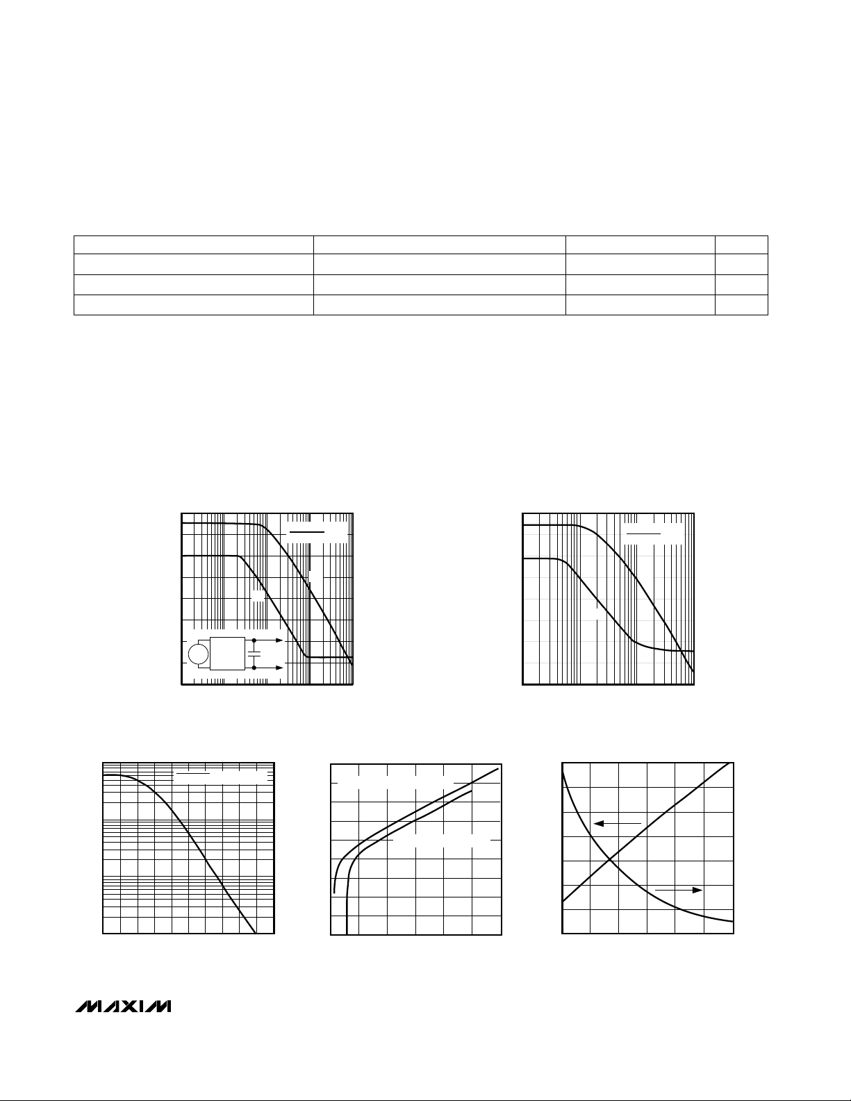
__________________________________________Typical Operating Characteristics
(TA = +25°C, unless otherwise noted.)
20
10
0
GAIN (dB)
-10
-20
CURRENT-SENSE AMPLIFIER
FREQUENCY RESPONSE (with 15pF)
C2 = 15pF
FASTCHG = 0V
A
Φ
BATT-
+
V
IN
-
GND
1k
CURRENT-
SENSE
AMP
FREQUENCY (Hz)
CC
BATT-
100k
V
OUT
+
-
1M10k 10M
40
MAX712/13 LOG1
0
V
-40
PHASE (DEGREES)
-80
-120
20
10
GAIN (dB)
-10
-20
CURRENT-SENSE AMPLIFIER
FREQUENCY RESPONSE (with 10nF)
0
Φ
10 1k
100 10k
FREQUENCY (Hz)
C2 = 10nF
FASTCHG = 0V
A
V
40
MAX712/13 LOG2
0
-40
PHASE (DEGREES)
-80
-120
MAX712/MAX713
CURRENT ERROR-AMPLIFIER
TRANSCONDUCTANCE
100
FASTCHG = 0V, V+ = 5V
10
1
DRV PIN SINK CURRENT(mA)
0.1
1.95 1.97 2.01 2.05
1.99 2.03
VOLTAGE ON CC PIN (V)
_______________________________________________________________________________________ 3
MAX712/13 LOG3
V+ VOLTAGE (V)
SHUNT-REGULATOR VOLTAGE
vs. CURRENT
5.8
DRV NOT SINKING CURRENT
5.6
5.4
5.2
5.0
4.8
4.6
4.4
4.2
4.0
10 20 50
060
DRV SINKING CURRENT
30
40
CURRENT INTO V+ PIN (mA)
MAX712/13 LOG4
ALPHA THERMISTOR PART No. 13A1002
STEINHART-HART INTERPOLATION
1.6
1.4
1.2
1.0
0.8
0.6
TEMP PIN VOLTAGE (V)
0.4
0.2
10 20 50
060
BATTERY TEMPERATURE(°C)
35
30
25
20
15
10
5
BATTERY THERMISTOR RESISTANCE (kΩ)
30
40
0
Page 4
NiCd/NiMH Battery
Fast-Charge Controllers
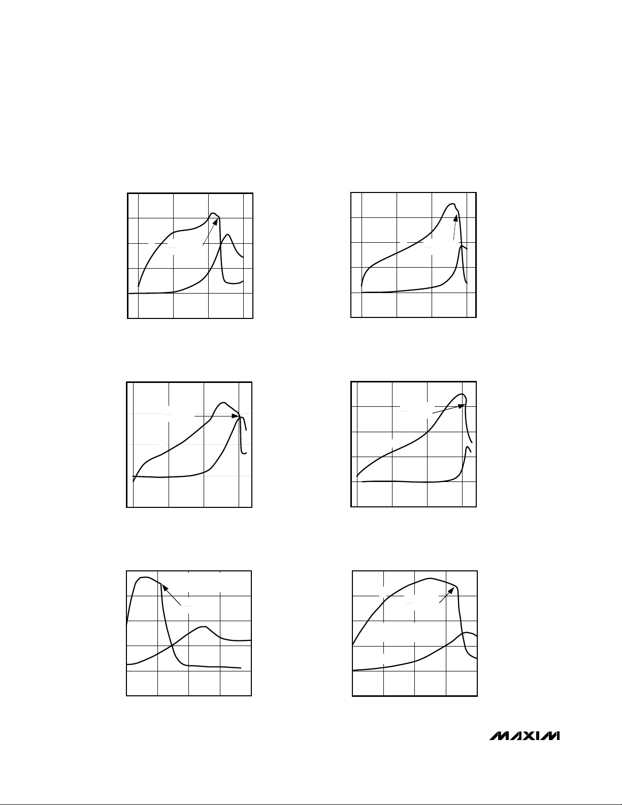
____________________________Typical Operating Characteristics (continued)
(TA = +25°C, unless otherwise noted.)
MAX713
NiCd BATTERY-CHARGING
CHARACTERISTICS AT C RATE
CHARACTERISTICS AT C RATE
MAX713
NiMH BATTERY-CHARGING
1.55
1.50
1.45
CELL VOLTAGE (V)
1.40
∆V
V
CUTOFF
∆t
T
MAX712/MAX713
0
CHARACTERISTICS AT C/2 RATE
1.50
1.45
CELL VOLTAGE (V)
1.40
30 9060
CHARGE TIME (MINUTES)
MAX713
NiCd BATTERY-CHARGING
∆V
CUTOFF
∆t
V
T
MAX712/713
40
35
30
25
MAX712/713
35
30
25
MAX712/713
1.60
1.55
1.50
CELL VOLTAGE (V)
CELL TEMPERATURE (°C)
1.45
0
30 9060
CHARGE TIME (MINUTES)
∆V
V
T
∆t
CUTOFF
40
35
30
CELL TEMPERATURE (°C)
25
MAX713
NiMH BATTERY-CHARGING
CHARACTERISTICS AT C/2 RATE
MAX712/713
1.55
1.50
1.45
CELL VOLTAGE (V)
CELL TEMPERATURE (°C)
1.40
∆V
CUTOFF
∆t
V
T
40
35
30
CELL TEMPERATURE (°C)
25
0
50 150100
CHARGE TIME (MINUTES)
MAX713
CHARGING CHARACTERISTICS OF A
FULLY CHARGED NiMH BATTERY
1.65
1.60
1.55
1.50
CELL VOLTAGE (V)
1.45
V
T
0
CHARGE TIME (MINUTES)
BETWEEN CHARGES
∆V
5152010
5-MINUTE REST
∆t
CUTOFF
MAX712/713
40
35
30
25
0
CHARGING CHARACTERISTICS OF A
1.65
1.60
1.55
1.50
CELL TEMPERATURE (°C)
CELL VOLTAGE (V)
1.45
0
50 150100
CHARGE TIME (MINUTES)
MAX713
FULLY CHARGED NiMH BATTERY
V
∆V
CUTOFF
∆t
5-HOUR REST
BETWEEN CHARGES
T
51510
CHARGE TIME (MINUTES)
4 _______________________________________________________________________________________
MAX712/713
40
35
30
CELL TEMPERATURE (°C)
25
20
Page 5
NiCd/NiMH Battery
Fast-Charge Controllers
______________________________________________________________Pin Description
PIN
3, 4
8
9, 10
VLIMIT1
PGM0,
PGM1
TLO6
FASTCHG
PGM2,
PGM3
Sets the maximum cell voltage. The battery terminal voltage (BATT+ - BATT-) will not exceed VLIMIT x
(number of cells). Do not allow VLIMIT to exceed 2.5V. Tie VLIMIT to VREF for normal operation.
Positive terminal of batteryBATT+2
PGM0 and PGM1 set the number of series cells to be charged. The number of cells can be set from
1 to 16 by connecting PGM0 and PGM1 to any of V+, REF, or BATT-, or by leaving the pin open (Table
2). For cell counts greater than 11, see the
or fewer cells than the number programmed may inhibit ∆V fast-charge termination.
Trip point for the over-temperature comparator. If the voltage-on TEMP rises above THI, fast charge ends.THI5
Trip point for the under-temperature comparator. If the MAX712/MAX713 power on with the voltage-on
TEMP less than TLO, fast charge is inhibited and will not start until TEMP rises above TLO.
Sense input for temperature-dependent voltage from thermistors.TEMP7
Open-drain, fast-charge status output. While the MAX712/MAX713 fast charge the battery, FASTCHG
sinks current. When charge ends and trickle charge begins, FASTCHG stops sinking current.
PGM2 and PGM3 set the maximum time allowed for fast charging. Timeouts from 33 minutes to 264
minutes can be set by connecting to any of V+, REF, or BATT-, or by leaving the pin open (Table 3).
PGM3 also sets the fast-charge to trickle-charge current ratio (Table 5).
Compensation input for constant current regulation loopCC11
FUNCTIONNAME
Linear-Mode, High Series Cell Count
section. Charging more
MAX712/MAX713
Negative terminal of batteryBATT-12
System ground. The resistor placed between BATT- and GND monitors the current into the battery.GND13
Current sink for driving the external PNP current sourceDRV14
V+15
Shunt regulator. The voltage on V+ is regulated to +5V with respect to BATT-, and the shunt current
powers the MAX712/MAX713.
2V reference outputREF16
_______________________________________________________________________________________ 5
Page 6
NiCd/NiMH Battery
Fast-Charge Controllers
____________________Getting Started
The MAX712/MAX713 are simple to use. A complete
linear-mode or switch-mode fast-charge circuit can be
designed in a few easy steps. A linear-mode design
uses the fewest components and supplies a load while
charging, while a switch-mode design may be necessary if lower heat dissipation is desired.
1) Follow the battery manufacturer’s recommendations
on maximum charge currents and charge-termination
methods for the specific batteries in your application.
Table 1 provides general guidelines.
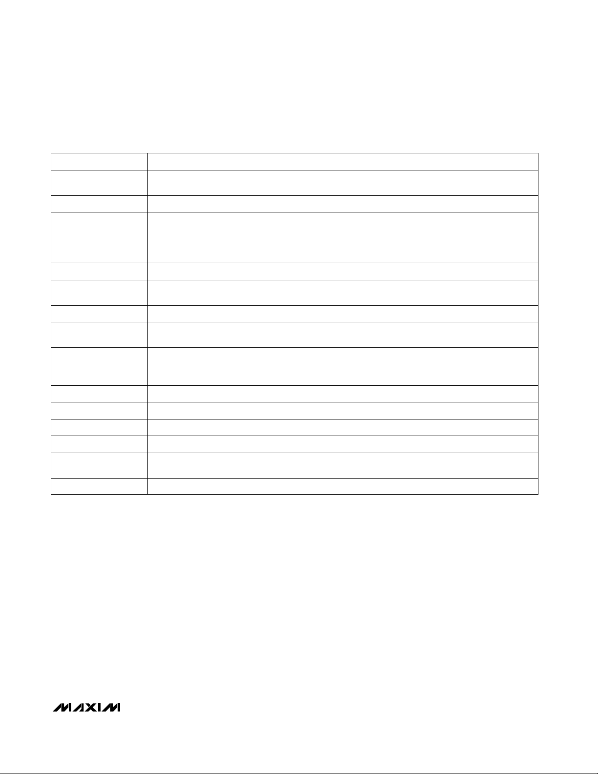
Table 1. Fast-Charge Termination Methods
Charge
MAX712/MAX713
Rate
> 2C
2C to C/2
< C/2
2) Decide on a charge rate (Tables 3 and 5). The slowest fast-charge rate for the MAX712/MAX713 is C/4,
because the maximum fast-charge timeout period is
264 minutes. A C/3 rate charges the battery in about
three hours. The current in mA required to charge at
this rate is calculated as follows:
Depending on the battery, charging efficiency can be
as low as 80%, so a C/3 fast charge could take 3 hours
and 45 minutes. This reflects the efficiency with which
electrical energy is converted to chemical energy within
the battery, and is not the same as the powerconversion efficiency of the MAX712/MAX713.
3) Decide on the number of cells to be charged (Table 2).
If your battery stack exceeds 11 cells, see the
Mode High Series Cell Count
changing the number of cells to be charged, PGM0
NiMH Batteries NiCd Batteries
∆V/∆t and
temperature,
MAX712 or MAX713
∆V/∆t and/or
temperature,
MAX712 or MAX713
∆V/∆t and/or
temperature, MAX712
I
= (capacity of battery in mAh)
FAST
–––––––––––––––––––––––
(charge time in hours)
∆V/∆t and/or
temperature, MAX713
∆V/∆t and/or
temperature, MAX713
∆V/∆t and/or
temperature, MAX713
section. Whenever
––
Linear-
and PGM1 must be adjusted accordingly. Attempting
to charge more or fewer cells than the number programmed can disable the voltage-slope fast-charge
termination circuitry. The internal ADC’s input voltage range is limited to between 1.4V and 1.9V (see
Electrical Characteristics
the
voltage across the battery divided by the number of
cells programmed (using PGM0 and PGM1, as in
Table 2). When the ADC’s input voltage falls out of
its specified range, the voltage-slope termination circuitry can be disabled.
4) Choose an external DC power source (e.g., wall
cube). Its minimum output voltage (including ripple)
must be greater than 6V and at least 1.5V higher (2V
for switch mode) than the maximum battery voltage
while charging. This specification is critical because
normal fast-charge termination is ensured only if this
requirement is maintained (see
MAX712/MAX713
5) For linear-mode designs, calculate the worst-case
power dissipation of the power PNP and diode (Q1
and D1 in the
using the following formula:
PD
load - minimum battery voltage) x (charge current
in amps)
If the maximum power dissipation is not tolerable for
your application, refer to the
use a switch-mode design (see
= (maximum wall-cube voltage under
PNP
Operation
and see the MAX713 EV kit manual).
6) For both linear and switch-mode designs, limit current into V+ to between 5mA and 20mA. For a fixed
or narrow-range input voltage, choose R1 in the
section for more details).
Typical Operating Circuit
in the
Applications Information
Typical Operation Circuit
R1 = (minimum wall-cube voltage - 5V) / 5mA
For designs requiring a large input voltage variation,
choose the current-limiting diode D4 in Figure 19.
7) Choose R
8) Consult Tables 2 and 3 to set pin-straps before
applying power. For example, to fast charge at a
rate of C/2, set the timeout to between 1.5x or 2x the
charge period, three or four hours, respectively.
using the following formula:
SENSE
RSENSE = 0.25V / (I
), and is equal to the
Powering the
) in watts,
Detailed Description
or
Switch-Mode
section,
using the following formula:
)
FAST
6 _______________________________________________________________________________________
Page 7

NiCd/NiMH Battery
Fast-Charge Controllers
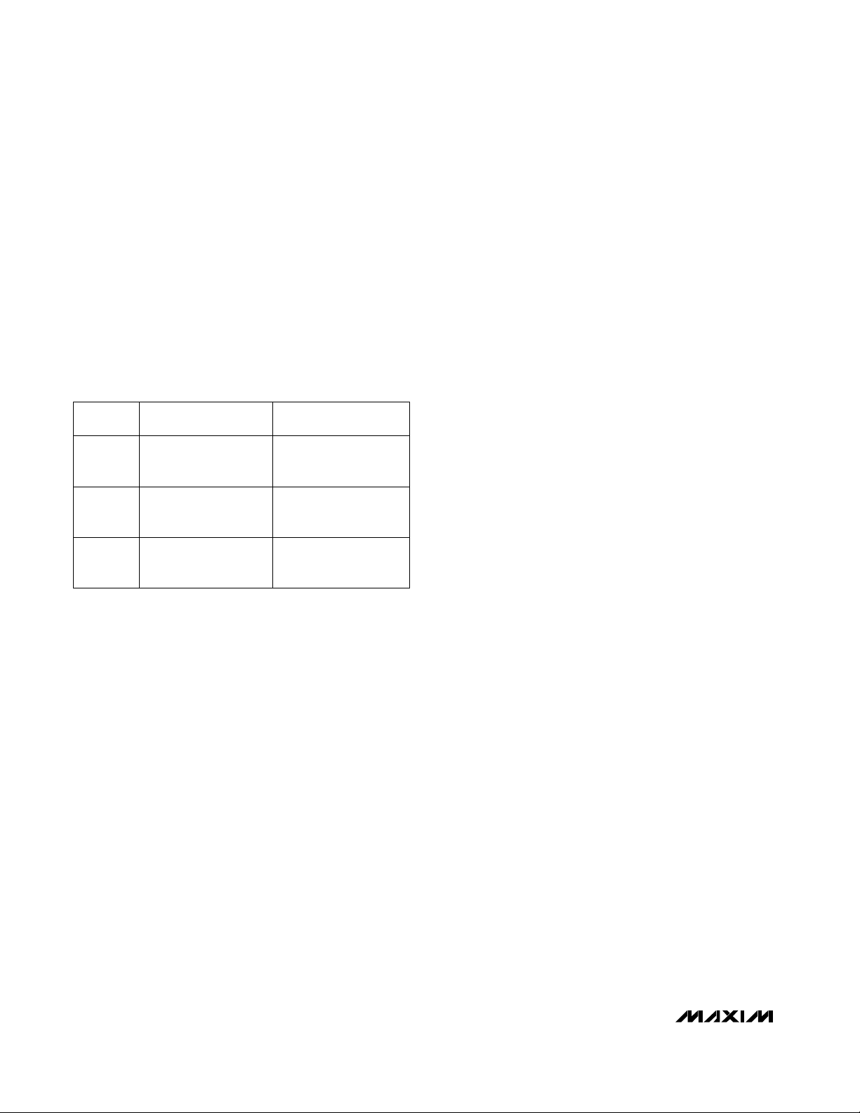
Table 2. Programming the Number
of Cells
Number
of Cells
1 V+ V+
2 Open V+
3 REF V+
4 BATT- V+
5 V+ Open
6 Open Open
7 REF Open
8 BATT- Open
9 V+ REF
10 Open REF
11 REF REF
12 BATT- REF
13 V+ BATT14 Open BATT15 REF BATT16 BATT- BATT-
PGM1 Connection PGM0 Connection
Table 3. Programming the Maximum
Charge Time
Timeout
(min)
22 V+ Open
22 V+ REF
33 V+ V+
33 V+ BATT45 Open Open
45 Open REF
66 Open V+
66 Open BATT90 REF Open
90 REF REF
132 REF V+
132 REF BATT180 BATT- Open
180 BATT- REF
264 BATT- V+
264 BATT- BATT-
A/D
Sampling
Interval
(sec) (tA)
21
21
21
21
42
42
42
42
84
84
84
84
168
168
168
168
Voltage-
Slope
Termination
Disabled
Enabled
Disabled
Enabled
Disabled
Enabled
Disabled
Enabled
Disabled
Enabled
Disabled
Enabled
Disabled
Enabled
Disabled
Enabled
PGM3
Connection
Connection
MAX712/MAX713
PGM2
PGM2 PGM3
TIMER
PGM2
PGM3
THI
TEMP
TLO
∆V
DETECTION
TEMPERATURE
COMPARATORS
Figure 1. Block Diagram
_______________________________________________________________________________________ 7
TIMED_OUT
∆V_DETECT
HOT
COLD
V+
BATT-
CONTROL LOGIC
MAX712
MAX713
+5V SHUNT
REGULATOR
POWER_ON_RESET
FAST_CHARGE
IN_REGULATION
UNDER_VOLTAGE
CELL_VOLTAGE
0.4V
BATT-
GND
N
BATT-
CURRENT
AND
VOLTAGE
REGULATOR
BATT-
FASTCHG
DRV
CC
BATTGND
VLIMIT
BATT+
PGM0
PGM1
INTERNAL IMPEDANCE OF PGM0–PGM3 PINS
PGMx
100k
100k
V+
REF
Page 8

NiCd/NiMH Battery
Fast-Charge Controllers
_______________Detailed Description
The MAX712/MAX713 fast charge NiMH or NiCd batteries by forcing a constant current into the battery. The
MAX712/MAX713 are always in one of two states: fast
charge or trickle charge. During fast charge, the
current level is high; once full charge is detected, the
current reduces to trickle charge. The device monitors
three variables to determine when the battery reaches
full charge: voltage slope, battery temperature, and
charge time.
1.5
1.4
MAX712/MAX713
1. NO POWER TO CHARGER
2. CELL VOLTAGE LESS THAN 0.4V
3. FAST CHARGE
4. TRICKLE CHARGE
5. CHARGER POWER REMOVED
1.3
0.4
CELL VOLTAGE (V)CURRENT INTO CELL
0
A
mA
µA
Figure 2. Typical Charging Using Voltage Slope
VOLTAGE
TEMPERATURE
1
2
TIME
4
53
Figure 1 shows the block diagram for the MAX712/
MAX713. The timer, voltage-slope detection, and temperature comparators are used to determine full charge
state. The voltage and current regulator controls output
voltage and current, and senses battery presence.
Figure 2 shows a typical charging scenario with batteries
already inserted before power is applied. At time 1, the
MAX712/MAX713 draw negligible power from the battery. When power is applied to DC IN (time 2), the
power-on reset circuit (see the POWER
nal in Figure 1) holds the MAX712/MAX713 in trickle
charge. Once POWER
enters the fast-charge state (time 3) as long as the cell
voltage is above the undervoltage lockout (UVLO) voltage (0.4V per cell). Fast charging cannot start until (battery voltage) / (number of cells) exceeds 0.4V.
When the cell voltage slope becomes negative, fast
CELL TEMPERATURE
charge is terminated and the MAX712/MAX713 revert
to trickle-charge state (time 4). When power is removed
(time 5), the device draws negligible current from the
battery.
Figure 3 shows a typical charging event using temperature full-charge detection. In the case shown, the battery pack is too cold for fast charging (for instance,
brought in from a cold outside environment). During
time 2, the MAX712/MAX713 remain in trickle-charge
state. Once a safe temperature is reached (time 3), fast
charge starts. When the battery temperature exceeds
the limit set by THI, the MAX712/MAX713 revert to trickle charge (time 4).
-
-
_ON
_RESET sig-
-
-
_ON
_RESET goes high, the device
VREF = VLIMIT
THI
TLO
CELL TEMPERATURECURRENT INTO CELL
A
mA
µA
1
1. NO POWER TO CHARGER
2. CELL TEMPERATURE TOO LOW
3. FAST CHARGE
4. TRICKLE CHARGE
243
TIME
Figure 3. Typical Charging Using Temperature
8 _______________________________________________________________________________________
1. BATTERY NOT INSERTED
2. FAST CHARGE
3. TRICKLE CHARGE
4. BATTERY REMOVED
Figure 4. Typical Charging with Battery Insertion
1.5
1.4
1.3
CELL VOLTAGE (V)CURRENT INTO CELL
A
mA
µA
1
243
TIME
Page 9

NiCd/NiMH Battery
IN_REGULATION
POWER_ON_RESET
COLD
HOT
Fast-Charge Controllers
The MAX712/MAX713 can be configured so that voltage
slope and/or battery temperature detects full charge.
Figure 4 shows a charging event in which a battery is
inserted into an already powered-up MAX712/MAX713.
the voltage on the battery pack is higher during a fastcharge cycle than while in trickle charge or while supplying a load. The voltage across some battery packs may
approach 1.9V/cell.
During time 1, the charger’s output voltage is regulated
at the number of cells times VLIMIT. Upon insertion of
the battery (time 2), the MAX712/MAX713 detect current flow into the battery and switch to fast-charge
DC IN
state. Once full charge is detected, the device reverts
to trickle charge (time 3). If the battery is removed (time
4), the MAX712/MAX713 remain in trickle charge and
the output voltage is once again regulated as in time 1.
Powering the MAX712/MAX713
AC-to-DC wall-cube adapters typically consist of a transformer, a full-wave bridge rectifier, and a capacitor.
Figures 10–12 show the characteristics of three consumer product wall cubes. All three exhibit substantial
120Hz output voltage ripple. When choosing an adapter
for use with the MAX712/MAX713, make sure the lowest
wall-cube voltage level during fast charge and full load is
at least 1.5V higher (2V for switch mode) than the maximum battery voltage while being fast charged. Typically,
Figure 5. DRV Pin Cascode Connection (for high DC IN voltage
or to reduce MAX712/MAX713 power dissipation in linear mode)
Table 4. MAX712/MAX713 Charge-State Transition Table
UNDER_VOLTAGE
0 x x
↑
↑
↑
↑
↑
1 0 0
1 0 0
1
1 0
1 0 0
1 0 0
1 x x
1 x x
1
1 0
1 x x x
1 x
x 1
x x
x x
0 0
↓
↑
0
↓
0
↑
x
x
x
0
x
1
1
↓
1
1
1
↑
0
x
x
x
R2
R1
V+ DRV
MAX712
MAX713
†
x
x
x
x
0
1
1
1
1
1
↑
1
x
0
x
x
↓
Set trickle
No change
No change
No change
No change***
Set fast
No change
No change
Set fast
Set fast
No change***
Set fast**
Trickle to fast transition inhibited
Trickle to fast transition inhibited
Set trickle
Set trickle
Set trickle
MAX712/MAX713
D1Q1
2N3904
Result*
†
Only two states exist: fast charge and trickle charge.
*
Regardless of the status of the other logic lines, a timeout or a voltage-slope detection will set trickle charge.
**
If the battery is cold at power-up, the first rising edge on COLD will trigger fast charge; however, a second rising edge will
have no effect.
***
Batteries that are too hot when inserted (or when circuit is powered up) will not enter fast charge until they cool and power is recycled.
_______________________________________________________________________________________ 9
Page 10

NiCd/NiMH Battery
Fast-Charge Controllers
DC IN
DRV
D1
MAX712/MAX713
BATT-
R
SENSE
GND
Figure 6. Current and Voltage Regulator (linear mode)
The 1.5V of overhead is needed to allow for worst-case
voltage drops across the pass transistor (Q1 of
Operating Circuit
resistor (R
ment is critical, because violating it can inhibit proper
termination of the fast-charge cycle. A safe rule of
thumb is to choose a source that has a minimum input
voltage = 1.5V + (1.9V x the maximum number of cells
to be charged). When the input voltage at DC IN drops
below the 1.5V + (1.9V x number of cells), the part
oscillates between fast charge and trickle charge and
might never completely terminate fast-charge.
The MAX712/MAX713 are inactive without the wall cube
attached, drawing 5µA (max) from the battery. Diode D1
prevents current conduction into the DRV pin. When the
wall cube is connected, it charges C1 through R1 (see
Typical Operating Circuit
(Figure 19). Once C1 charges to 5V, the internal shunt
SENSE
V+
REF
VLIMIT
GND
CURRENT-SENSE AMPLIFIER
PGM3 FAST_CHARGE Av
OPEN
BATT-
V+
REF
1
X
0
0
0
0
CELL_VOLTAGE
8
512
256
128
64
BATT-
IN_REGULATION
1.25V
BATT-
), the diode (D1), and the sense
). This minimum input voltage require-
) or the current-limiting diode
Typical
CC
BATT-
regulator sinks current to regulate V+ to 5V, and fast
charge commences. The MAX712/MAX713 fast charge
until one of the three fast-charge terminating conditions
is triggered.
If DC IN exceeds 20V, add a cascode connection in
series with the DRV pin as shown in Figure 5 to prevent
exceeding DRV’s absolute maximum ratings.
Furthermore, if Figure 19’s DC IN exceeds 15V, a transistor level-shifter is needed to provide the proper voltage swing to the MOSFET gate. See the MAX713 EV kit
manual for details.
Select the current-limiting component (R1 or D4) to
pass at least 5mA at the minimum DC IN voltage (see
step 6 in the
Getting Started
section). The maximum
current into V+ determines power dissipation in the
MAX712/MAX713.
maximum current into V+ =
(maximum DC IN voltage - 5V) / R1
power dissipation due to shunt regulator =
C2
5V x (maximum current into V+)
Sink current into the DRV pin also causes power dissipation. Do not allow the total power dissipation to exceed
the specifications shown in the
Ratings
.
Absolute Maximum
Fast Charge
The MAX712/MAX713 enter the fast-charge state under
one of the following conditions:
1) Upon application of power (batteries already
installed), with battery current detection (i.e., GND
voltage is less than BATT- voltage), and TEMP
higher than TLO and less than THI and cell voltage
higher than the UVLO voltage.
2) Upon insertion of a battery, with TEMP higher than
TLO and lower than THI and cell voltage higher than
the UVLO voltage.
R
sets the fast-charge current into the battery. In
SENSE
fast charge, the voltage difference between the BATTand GND pins is regulated to 250mV. DRV current
increases its sink current if this voltage difference falls
below 250mV, and decreases its sink current if the voltage difference exceeds 250mV.
fast-charge current (I
) = 0.25V / R
FAST
SENSE
Trickle Charge
Selecting a fast-charge current (I
4C ensures a C/16 trickle-charge current. Other fastcharge rates can be used, but the trickle-charge
current will not be exactly C/16.
) of C/2, C, 2C, or
FAST
10 ______________________________________________________________________________________
Page 11

NiCd/NiMH Battery
Fast-Charge Controllers
Table 5. Trickle-Charge Current
Determination from PGM3
PGM3
V+ 4C I
OPEN 2C I
REF C I
BATT- C/2 I
Fast-Charge Rate
The MAX712/MAX713 internally set the trickle-charge
current by increasing the current amplifier gain (Figure
6), which adjusts the voltage across R
Trickle-Charge V
SENSE
in the
Electrical Characteristics
table).
Nonstandard Trickle-Charge
Configuration:
Typical Operating Circuit
2 x Panasonic P-50AA 500mAh AA NiCd batteries
C/3 fast-charge rate
264-minute timeout
Negative voltage-slope cutoff enabled
Minimum DC IN voltage of 6V
Settings:
Use MAX713
PGM0 = V+, PGM1 = open, PGM2 = BATT-,
PGM3 = BATT-, R
I
= 167mA), R1 = (6V - 5V) / 5mA = 200Ω
FAST
= 1.5Ω (fast-charge current,
SENSE
Since PGM3 = BATT-, the voltage on R
ed to 31.3mV during trickle charge, and the current is
20.7mA. Thus the trickle current is actually C/25, not
C/16.
Further Reduction of Trickle-Charge
Current for NiMH Batteries
The trickle-charge current can be reduced to less than
C/16 using the circuit in Figure 7. In trickle charge,
some of the current will be shunted around the battery,
since Q2 is turned on. Select the value of R7 as follows:
R7 = (V
where V
BATT
I
TRlCKLE
current setting
I
BATT
+ 0.4V) / (l
BATT
TRlCKLE
= battery voltage when charged
= MAX712/MAX713 trickle-charge
= desired battery trickle-charge current
Trickle-Charge
Current (I
FAST
FAST
FAST
FAST
TRICKLE
SENSE
)
/64
/32
/16
/8
(see
Current Example
is regulat-
SENSE
- I
)
BATT
DC IN
DRV
MAX712
MAX713
GND
Figure 7. Reduction of Trickle Current for NiMH Batteries
(linear mode)
FASTCHG
V+
10k
10k
D1Q1
R7
BATTERY
Q2
R
SENSE
Regulation Loop
The regulation loop controls the output voltage between
the BATT+ and BATT- terminals and the current
through the battery via the voltage between BATT- and
GND. The sink current from DRV is reduced when the
output voltage exceeds the number of cells times
V
, or when the battery current exceeds the pro-
LIMIT
grammed charging current.
For a linear-mode circuit, this loop provides the following
functions:
1) When the charger is powered, the battery can be
removed without interrupting power to the load.
2) If the load is connected as shown in the
Operating Circuit
, the battery current is regulated
Typical
regardless of the load current (provided the input
power source can supply both).
Voltage Loop
The voltage loop sets the maximum output voltage
between BATT+ and BATT-. If V
2.5V, then:
Maximum BATT+ voltage (referred to BATT-) = V
(number of cells as determined by PGM0, PGM1)
VLIMIT should be set between 1.9V and 2.5V. If VLIMIT
is set below the maximum cell voltage, proper
termination of the fast-charge cycle might not occur.
Cell voltage can approach 1.9V/cell, under fast charge,
in some battery packs. Tie V
LIMIT
operation .
With the battery removed, the MAX712/MAX713 do not
provide constant current; they regulate BATT+ to the
maximum voltage as determined above.
is set to less than
LIMIT
to V
REF
LIMIT
for normal
x
MAX712/MAX713
______________________________________________________________________________________ 11
Page 12

NiCd/NiMH Battery
Fast-Charge Controllers
The voltage loop is stabilized by the output filter
capacitor. A large filter capacitor is required only if the
load is going to be supplied by the MAX712/MAX713 in
the absence of a battery. In this case, set C
C
OUT
where BW
(in farads) = (50 x I
= loop bandwidth in Hz
VRL
LOAD
) / (V
OUT
OUT
x BW
VRL
(10,000 recommended)
C
> 10µF
OUT
I
= external load current in amps
LOAD
V
= programmed output voltage
OUT
(V
x number of cells)
LIMIT
Current Loop
Figure 6 shows the current-regulation loop for a linearmode circuit. To ensure loop stability, make sure that
MAX712/MAX713
the bandwidth of the current regulation loop (BW
lower than the pole frequency of transistor Q1 (fB). Set
BW
by selecting C2.
CRL
BW
CRL
in Hz = gm / C2, C2 in farads,
gm = 0.0018 Siemens
The pole frequency of the PNP pass transistor, Q1, can
be determined by assuming a single-pole current gain
response. Both fTand Boshould be specified on the
data sheet for the particular transistor used for Q1.
fBin Hz = fT/ Bo, fTin Hz, Bo= DC current gain
Condition for Stability of Current-Regulation Loop:
BW
CRL
< f
B
The MAX712/MAX713 dissipate power due to the current-voltage product at DRV. Do not allow the power
dissipation to exceed the specifications shown in the
Absolute Maximum Ratings
. DRV power dissipation can
be reduced by using the cascode connection shown in
Figure 5 or by using a switch-mode circuit.
Power dissipation due to DRV sink current =
(current into DRV) x (voltage on DRV)
Voltage-Slope Cutoff
The MAX712/MAX713’s internal analog-to-digital converter has 2.5mV of resolution. It determines if the battery voltage is rising, falling, or unchanging by
comparing the battery’s voltage at two different times.
After power-up, a time interval of tAranging from 21sec
to 168sec passes (see Table 3 and Figure 8), then a
battery voltage measurement is taken. It takes 5ms to
perform a measurement. After the first measurement is
complete, another tAinterval passes, and then a
second measurement is taken. The two measurements
are compared, and a decision whether to terminate
charge is made. If charge is not terminated, another full
two-measurement cycle is repeated until charge is
as:
CRL
terminated. Note that each cycle has two tAintervals
and two voltage measurements.
The MAX712 terminates fast charge when a comparison shows that the battery voltage is unchanging. The
)
MAX713 terminates when a conversion shows the battery voltage has fallen by at least 2.5mV per cell. This is
the only difference between the MAX712 and MAX713.
Temperature Charge Cutoff
Figure 9a shows how the MAX712/MAX713 detect overand under-temperature battery conditions using negative
temperature coefficient thermistors. Use the same model
thermistor for T1 and T2 so that both have the same
nominal resistance. The voltage at TEMP is 1V (referred
to BATT-) when the battery is at ambient temperature.
The threshold chosen for THI sets the point at which
) is
fast charging terminates. As soon as the voltage-on
TEMP rises above THI, fast charge ends, and does not
restart after TEMP falls below THI.
The threshold chosen for TLO determines the temperature below which fast charging will be inhibited.
If TLO > TEMP when the MAX712/MAX713 start up, fast
charge will not start until TLO goes below TEMP.
The cold temperature charge inhibition can be disabled
by removing R5, T3, and the 0.022µF capacitor; and by
tying TLO to BATT-.
To disable the entire temperature comparator chargecutoff mechanism, remove T1, T2, T3, R3, R4, and R5,
and their associated capacitors, and connect THI to V+
and TLO to BATT-. Also, place a 68kQ resistor from
REF to TEMP, and a 22kΩresistor from BATT- to TEMP.
Some battery packs come with a temperature-detecting
thermistor connected to the battery pack’s negative
ZERO
VOLTAGE
COUNTS
Figure 8. Voltage Slope Detection
VOLTAGE
RISES
0t
5ms 5ms 5ms 5ms 5ms 5ms
t
INTERVAL
NOTE: SLOPE PROPORTIONAL TO VBATT
t
A
A
INTERVAL INTERVAL INTERVAL INTERVAL INTERVAL
SLOPE
CUTOFF FOR MAX712
POSITIVE
RESIDUAL
t
t
A
A
NEGATIVE
VOLTAGE
SLOPE
CUTOFF FOR MAX712
OR MAX713
ZERO
RESIDUAL
t
A
t
A
NEGATIVE
RESIDUAL
12 ______________________________________________________________________________________
Page 13

NiCd/NiMH Battery
Fast-Charge Controllers
IN THERMAL
CONTACT WITH
TEMPERATURE
R5
BATTERY
AMBIENT
T3
0.022µF
REF
R3
THI
HOT
R4
+2.0V
TEMP
COLD
TLO
0.022µF
MAX712
MAX713
BATT-
AMBIENT
TEMPERATURE
NOTE: FOR ABSOLUTE TEMPERATURE CHARGE CUTOFF, T2 AND T3 CAN BE
REPLACED BY STANDARD RESISTORS.
Figure 9a. Temperature Comparators
AMBIENT
REF
TEMPERATURE
terminal. In this case, use the configuration shown in
MAX712/MAX713
Figure 9b. Thermistors T2 and T3 can be replaced by
standard resistors if absolute temperature charge cutoff is acceptable. All resistance values in Figures 9a
and 9b should be chosen in the 10kΩto 500kΩrange.
T1
__________Applications Information
Switch-Mode Operation
For applications where the power dissipation in the
pass transistor cannot be tolerated (ie., where heat
sinking is not feasible or is too costly), a switch-mode
T2
1µF
charger is recommended.
Switch-mode operation can be implemented simply by
using the circuit of Figure 19. The circuit of Figure 19
uses the error amplifier at the CC pin as a comparator
with the 33pF capacitor adding hysteresis. Figure 19 is
shown configured to charge two cells at 1A. Lower
charge currents and a different number of cells can be
accommodated simply by changing R
SENSE
and
PGM0–PGM3 connections (Tables 2 and 3).
The input power-supply voltage range is 8V to 15V and
must be at least 2V greater than the peak battery
voltage, under fast charge. As shown in Figure 19, the
source should be capable of greater than 1.3A of
output current. The source requirements are critical
because if violated, proper termination of the fastcharge cycle might not occur. For input voltages
greater than 15V, see the MAX713SWEVKIT data sheet.
T2
HOT
+2.0V
COLD
MAX712
MAX713
NOTE: FOR ABSOLUTE TEMPERATURE CHARGE CUTOFF, T2 AND T3 CAN BE
REPLACED BY STANDARD RESISTORS.
THI
TEMP
TLO
BATT-
0.022µF
0.022µF
T1
IN THERMAL
CONTACT WITH
BATTERY
R3R5
1µF
R4
T3
AMBIENT
TEMPERATURE
Figure 9b. Alternative Temperature Comparator Configuration
______________________________________________________________________________________ 13
11
MAX712/713
10
HIGH PEAK
9
8
OUTPUT VOLTAGE (V)
7
6
0 200 600 1000
400
LOAD CURRENT (mA)
120Hz RIPPLE
LOW PEAK
800
Figure 10. Sony Radio AC Adapter AC-190 Load Characteristic,
9VDC 800mA
Page 14

NiCd/NiMH Battery
Fast-Charge Controllers
The voltage-slope, fast-charge termination circuitry
might become disabled if attempting to charge a
different number of cells than the number programmed.
The switching frequency (nominally 30kHz) can be
decreased by increasing the value of the capacitor
connected between CC and BATT-. Make sure that
the two capacitors connected to the CC node are
placed as close as possible to the CC pin on the
MAX712/MAX713 and that their leads are of minimum
length. The CC node is a high-impedance point, so do
not route logic lines near the CC pin. The circuit of
Figure 19 cannot service a load while charging.
Order the MAX713SWEVKIT-SO for quick evaluation of
the MAX712/MAX713 in switch-mode operation. For
more information on switch-mode operation and
ordering information for external components, order the
MAX712/MAX713
MAX713EVKIT data sheet.
11
10
9
8
7
OUTPUT VOLTAGE (V)
6
5
0 200 600 1000
HIGH PEAK
LOW PEAK
400
LOAD CURRENT (mA)
120Hz
RIPPLE
800
Figure 11. Sony CD Player AC Adapter AC-96N Load
Characteristic, 9VDC 600mA
MAX712/713
Battery-Charging Examples
Figures 13 and 14 show the results of charging 3 AA,
1000mAh, NiMH batteries from Gold Peak (part no.
GP1000AAH, GP Batteries (619) 438-2202) at a 1A rate
using the MAX712 and MAX713, respectively. The
Typical Operating Circuit
thermistor configuration .
DC IN = Sony AC-190 +9VDC at 800mA AC-DC adapter
PGM0 = V+, PGM1 = REF, PGM2 = REF, PGM3 = REF
R1 = 200Ω, R2 = 150Ω, R
C1 = 1µF, C2 = 0.01µF, C3 = 10µF, V
R3 = 10kΩ, R4 = 15kΩ
T1, T2 = part #13A1002 (Alpha Thermistor: (800) 235-5445)
R5 omitted, T3 omitted, TLO = BATT-
18
16
14
12
OUTPUT VOLTAGE (V)
10
8
Figure 12. Panasonic Modem AC Adapter KX-A11 Load
Characteristic, 12VDC 500mA
LOW PEAK
0 200 600
LOAD CURRENT (mA)
is used with Figure 9a’s
= 0.25Ω
SENSE
120Hz
RIPPLE
400
HIGH PEAK
LIMIT
= REF
800
MAX712/713
5.0
4.9
4.8
4.7
4.6
4.5
BATTERY VOLTAGE (V)
4.4
4.3
4.2
030 90
∆V
∆t
V
TIME (MINUTES)
CUTOFF
T
60
Figure 13. 3 NiMH Cells Charged with MAX712
40
MAX712/713
38
36
34
32
30
28
26
24
BATTERY TEMPERATURE (°C)
Figure 14. NiMH Cells Charged with MAX713
5.0
4.9
4.8
4.7
4.6
4.5
BATTERY VOLTAGE (V)
4.4
4.3
4.2
030 90
∆V
∆t
V
TIME (MINUTES)
CUTOFF
T
60
14 ______________________________________________________________________________________
40
MAX712/713
38
36
34
32
30
28
26
24
BATTERY TEMPERATURE (°C)
Page 15

NiCd/NiMH Battery
Fast-Charge Controllers
Linear-Mode, High Series Cell Count
The absolute maximum voltage rating for the BATT+ pin
is higher when the MAX712/MAX713 are powered on. If
more than 11 cells are used in the battery, the BATT+
input voltage must be limited by external circuitry when
DC IN is not applied (Figure 15).
Efficiency During Discharge
The current-sense resistor, R
efficiency loss during battery use. The efficiency loss is
Q1
DC IN
R2
150Ω
500Ω
DRV
, causes a small
SENSE
D1
33k
Q2
TO
BATTERY
POSITIVE
TERMINAL
significant only if R
SENSE
is much greater than the
battery stack’s internal resistance. The circuit in Figure
16 can be used to shunt the sense resistor whenever
power is removed from the charger.
Status Outputs
Figure 17 shows a circuit that can be used to indicate
charger status with logic levels. Figure 18 shows a
circuit that can be used to drive LEDs for power and
charger status.
OV = NO POWER
5V = POWER
V
CC
OV = FAST
= TRICKLE OR
V
CC
NO POWER
MAX712
MAX712
MAX713
MAX713
V+
10k
FASTCHG
MAX712/MAX713
MAX712
MAX713
BATT+
Figure 15. Cascoding to Accommodate High Cell Counts for
Linear-Mode Circuits
D1
>4 CELLS
MAX712
MAX713
100k
V+
Figure 16. Shunting R
100k
*
GND
for Efficiency Improvement
SENSE
R
SENSE
LOW R
*
ON
LOGIC LEVEL
N-CHANNEL
POWER
MOSFET
Figure 17. Logic-Level Status Outputs
DC IN
R1
CHARGE POWER
V+
MAX712
470ΩMIN
MAX713
FAST CHARGE
FASTCHG
Figure 18. LED Connection for Status Outputs
______________________________________________________________________________________ 15
Page 16

NiCd/NiMH Battery
Fast-Charge Controllers
DC IN
8V TO 15V
3
Q4
CMPTA06
MAX712/MAX713
1
2
REF
68k
22k
C1
1µF
10V
C5
10µF
50V
D4
CCLHM080
(8mA CURRENT-
LIMITING DIODE)
R6
Ω
R7
Ω
R5
5
15
3
4
9
10
16
1
7
C4
0.1µF
THI
V+
PGM0
PGM1
PGM2
PGM3
REF
VLIMIT
TEMP
C6
10µF
50V
R2
5.1k
14
DRV
MAX713
FASTCHG
1
1
8
Q1
CMPTA06
2
Q2
2N2907
3
11
CC
BATT+
BATT-
3
2
TLD
GND
M1
IRFR9024
2
12
6
13
L1
D03340
220µH
D2
MBRS340T3
C2
220pF
R3
Ω
0.25
MBRS340T3
D1
2 x 1000mA-Hr
NiCd CELLS
C3
10µF
50V
BATT +
BATT–
470
Ω
Figure 19. Simplest Switch-Mode Charger
16 ______________________________________________________________________________________
Page 17

NiCd/NiMH Battery
Fast-Charge Controllers
_Ordering Information (continued) ___________________Chip Topography
PART
MAX713CPE
MAX713CSE
MAX713C/D 0°C to +70°C
MAX713EPE
MAX713ESE
MAX713MJE -55°C to +125°C
*
Contact factory for dice specifications.
**
Contact factory for availability and processing to MIL-STD-883.
TEMP. RANGE PIN-PACKAGE
0°C to +70°C
0°C to +70°C
-40°C to +85°C 16 Plastic DIP
-40°C to +85°C
16 Plastic DIP
16 Narrow SO
Dice*
16 Narrow SO
16 CERDIP**
PGM0
PGM1
TLO
BATT+ VLIMIT REF V+
DRV
GND
0.126
(3.200mm)
BATT-
THI
CC
PGM3
MAX712/MAX713
TEMP FASTCHG PGM2
0.80"
(2.032mm)
TRANSISTOR COUNT: 2193
SUBSTRATE CONNECTED TO V+
______________________________________________________________________________________ 17
Page 18

NiCd/NiMH Battery
Fast-Charge Controllers
MAX712/MAX713
NOTES
18 ______________________________________________________________________________________
 Loading...