

Page 1
General Description
The MAX7033 fully integrated low-power CMOS superheterodyne receiver is ideal for receiving amplitudeshift-keyed (ASK) data in the 300MHz to 450MHz
frequency range. The receiver has an RF input signal
range of -114dBm to 0dBm. With few external components and a low-current power-down mode, it is ideal
for cost-sensitive and power-sensitive applications typical in the automotive and consumer markets. The
MAX7033 consists of a low-noise amplifier (LNA), a fully
differential image-rejection mixer, an on-chip phaselocked loop (PLL) with integrated voltage-controlled
oscillator (VCO), a 10.7MHz IF limiting amplifier stage
with received-signal-strength indicator (RSSI), and analog baseband data-recovery circuitry. The MAX7033
also has a discrete one-step automatic gain control
(AGC) that reduces the LNA gain by 35dB when the RF
input signal exceeds -62dBm. The AGC circuitry offers
an externally controlled hold feature.
The MAX7033 is available in 28-pin TSSOP and
32-pin TQFN packages and is specified over the
extended (-40°C to +105°C) temperature range.
Features
o Optimized for 315MHz or 433MHz Band
o Operates from Single +3.3V or +5.0V Supplies
o High Dynamic Range with On-Chip AGC
o AGC Hold Circuit
o 1ms AGC Release Time
o Selectable Image-Rejection Center Frequency
o Selectable x64 or x32 f
LO/fXTAL
Ratio
o Low 5.2mA Operating Supply Current
o < 3.5µA Low-Current Power-Down Mode for
Efficient Power Cycling
o 250µs Startup Time
o Built-In 44dB RF Image Rejection
o Better than -114dBm Receive Sensitivity
o -40°C to +105°C Operation
MAX7033
315MHz/433MHz ASK Superheterodyne
Receiver with AGC Lock
________________________________________________________________
Maxim Integrated Products
1
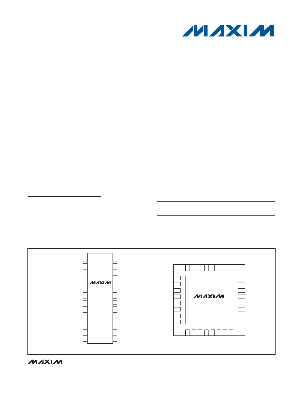
Pin Configurations
Ordering Information
Applications
19-3273; Rev 3; 9/11
For pricing, delivery, and ordering information, please contact Maxim Direct at 1-888-629-4642,
or visit Maxim’s website at www.maxim-ic.com.
+
Denotes a lead(Pb)-free/RoHS-compliant package.
*
EP = Exposed pad.
Typical Application Circuit appears at end of data sheet.
Automotive Remote
Keyless Entry
Security Systems
Garage Door Openers
Home Automation
Remote Controls
Local Telemetry
Wireless Sensors
TOP VIEW
LNASRC
LNAOUT
MIXOUT
+
1
XTAL1
2
AVDD
3
LNAIN
4
5
AGND
6
7
AVDD
8
MIXIN1
9
MIXIN2
10
AGND
11
IRSEL
12
13
DGND
14
DVDD
MAX7033
TSSOP
28
27
26
25
24
23
22
21
20
19
18
17
16
15
XTAL2
SHDN
PDOUT
DATAOUT
V
DD5
DSP
DFFB
OPP
DSN
DFO
IFIN2
IFIN1
XTALSEL
AC
PART TEMP RANGE PIN-PACKAGE
MAX7033EUI+ -40°C to +105°C 28 TSSOP
MAX7033ETJ+ -40°C to +105°C 32 TQFN-EP*
AVDD
XTAL1
XTAL2
SHDN
282726
131415
N.C.
XTALSEL
PDOUT
IFIN1
25 N.C.
16IFIN2
24 DATAOUT
23
V
DD5
22
DSP
21
N.C.
20
DFFB
19
OPP
18
DSN
17
DFO
AGND
LNAOUT
AVDD
MIXIN1
MIXIN2
AGND
IRSEL
LNASRC
LNAIN
32
313029
+
1N.C.
2
3
4
9
MIXOUT
MAX7033
101112
DVDD
DGND
TQFN
AC
5
6
7
8
Page 2
MAX7033
315MHz/433MHz ASK Superheterodyne
Receiver with AGC Lock
2 _______________________________________________________________________________________
ABSOLUTE MAXIMUM RATINGS
DC ELECTRICAL CHARACTERISTICS (+3.3V OPERATION)
(
Typical Application Circuit
, V
AVDD
= V
DVDD
= V
DD5
= +3.0V to +3.6V, no RF signal applied, TA= -40°C to +105°C, unless otherwise
noted. Typical values are at V
AVDD
= V
DVDD
= V
DD5
= +3.3V and TA= +25°C.) (Note 1)
Stresses beyond those listed under “Absolute Maximum Ratings” may cause permanent damage to the device. These are stress ratings only, and functional
operation of the device at these or any other conditions beyond those indicated in the operational sections of the specifications is not implied. Exposure to
absolute maximum rating conditions for extended periods may affect device reliability.
V
DD5
to AGND.......................................................-0.3V to +6.0V
AVDD to AGND .....................................................-0.3V to +4.0V
DVDD to DGND .....................................................-0.3V to +4.0V
AGND to DGND.....................................................-0.1V to +0.1V
IRSEL, DATAOUT, XTALSEL,
AC, SHDN to AGND .............................-0.3V to (V
DD5
+ 0.3V)
All Other Pins to AGND ..........................-0.3V to (V
DVDD
+ 0.3V)
Continuous Power Dissipation (T
A
= +70°C)
28-Pin TSSOP (derate 12.8mW/°C above +70°C) ..1025.6mW
32-Thin QFN (derate 21.3mW/°C above +70°C) ....1702.1mW
Operating Temperature Range .........................-40°C to +105°C
Junction Temperature......................................................+150°C
Storage Temperature Range .............................-60°C to +150°C
Lead Temperature (soldering 10s) ..................................+300°C
Soldering Temperature (reflow) .......................................+260°C
DC ELECTRICAL CHARACTERISTICS (+5.0V OPERATION)
(
Typical Application Circuit
, V
DD5
= +4.5V to +5.5V, no RF signal applied, TA= -40°C to +105°C, unless otherwise noted. Typical
values are at V
DD5
= +5.0V and TA= +25°C.) (Note 1)
PARAMETER SYMBOL CONDITIONS MIN TYP MAX UNITS
Supply Voltage
Supply Current I
Shutdown Supply Current I
Input-Voltage Low V
Input-Voltage High V
Input Logic Current High I
Image-Reject Select Voltage
(Note 2)
DATAOUT Output-Voltage Low V
DATAOUT Output-Voltage High V
V
AVDD
V
DVDD
DD
SHDN
,
+3.3V nominal supply voltage 3.0 3.3 3.6 V
fRF = 315MHz 5.2 6.23
fRF = 433MHz 5.7 6.88
fRF = 315MHz 2.6
f
= 433MHz 3.5 8.0
RF
= V
IRSEL
IRSEL
IRSEL
DD5
= V
/2 1.1
DD5
= 0V 0.4
IL
IH
IH
OL
OH
V
= V
SHDN
V
SHDN
V
XTALSEL
DVDD
= 0V,
= 0V
fRF = 433MHz, V
fRF = 375MHz, V
= 315MHz, V
f
RF
I
= 10μA 0.125 V
SINK
I
SOURCE
= 10μA
V
DVDD
- 0.4
V
DD5
0.4
10 μA
-
V
DVDD
- 0.125
0.4 V
V
-
DD5
1.0
mA
μA
V
V
V
PARAMETER SYMBOL CONDITIONS MIN TYP MAX UNITS
Supply Voltage V
Supply Current I
Shutdown Supply Current I
Input-Voltage Low V
DD5
DD
SHDN
+5.0V nominal supply voltage 4.5 5.0 5.5 V
V
= V
SHDN
V
SHDN
V
XTALSEL
IL
DD5
= 0V,
= 0V
fRF = 315MHz 5.2 6.4
fRF = 433MHz 5.7 6.76
fRF = 315MHz 3.7
f
= 433MHz 4.2 9.8
RF
mA
μA
0.4 V
Page 3
MAX7033
315MHz/433MHz ASK Superheterodyne
Receiver with AGC Lock
_______________________________________________________________________________________ 3
DC ELECTRICAL CHARACTERISTICS (+5.0V OPERATION) (continued)
(
Typical Application Circuit
, V
DD5
= +4.5V to +5.5V, no RF signal applied, TA= -40°C to +105°C, unless otherwise noted. Typical
values are at V
DD5
= +5.0V and TA= +25°C.) (Note 1)
AC ELECTRICAL CHARACTERISTICS
(
Typical Application Circuit
, V
AVDD
= V
DVDD
= V
DD5
= +3.0V to +3.6V, all RF inputs are referenced to 50Ω, fRF= 315MHz,
T
A
= -40°C to +105°C, unless otherwise noted. Typical values are at V
AVDD
= V
DVDD
= V
DD5
= +3.3V and TA= +25°C.) (Note 1)
Input-Voltage High V
Input Logic Current High I
Image-Reject Select Voltage
(Note 2)
DATAOUT Output-Voltage Low V
DATAOUT Output-Voltage High V
PARAMETER SYMBOL CONDITIONS MIN TYP MAX UNITS
V
-
V
DD5
0.4
DD5
0.4
15 μA
-
V
V
-
DD5
0.125
IH
IH
OL
OH
fRF = 433MHz, V
fRF = 375MHz, V
f
= 315MHz, V
RF
I
= 10μA 0.125 V
SINK
I
SOURCE
= 10μA
= V
IRSEL
IRSEL
IRSEL
DD5
= V
/2 1.1
DD5
= 0V 0.4
DD5
1.5
-
GENERAL CHARACTERISTICS
Startup Time t
Receiver Input Frequency f
Maximum Receiver Input Level Modulation depth >18dB 0 dBm
Sensitivity (Note 3)
AGC Hysteresis
Maximum Data Rate
LNA IN HIGH-GAIN MODE
1dB Compression Point P1dB
Input-Referred 3rd-Order
Intercept
LO Signal Feedthrough to
Antenna
Noise Figure NF
PARAMETER SYMBOL CONDITIONS MIN TYP MAX UNITS
IIP3
ON
RF
IN_LNA
LNA
LNA
LNA
Time for valid signal detection after V
= V
DVDD
Average carrier power level -120
Peak power level -114
LNA gain from low to high 8 dB
Switching time from low to high gain 1 ms
Manchester coded 33
NRZ coded 66
Normalized to 50Ω
fRF = 433MHz 1 - j3.4
fRF = 375MHz 1 - j3.9Input Impedance Z
= 315MHz 1 - j4.7
f
RF
SHDN
300 450 MHz
250 μs
-22 dBm
-12 dBm
-80 dBm
3dB
V
V
V
dBm
kbps
Page 4
MAX7033
315MHz/433MHz ASK Superheterodyne
Receiver with AGC Lock
4 _______________________________________________________________________________________
AC ELECTRICAL CHARACTERISTICS (continued)
(
Typical Application Circuit
, V
AVDD
= V
DVDD
= V
DD5
= +3.0V to +3.6V, all RF inputs are referenced to 50Ω, fRF= 315MHz,
T
A
= -40°C to +105°C, unless otherwise noted. Typical values are at V
AVDD
= V
DVDD
= V
DD5
= +3.3V and TA= +25°C.) (Note 1)
LNA IN LOW-GAIN MODE
Input Impedance Z
PARAMETER SYMBOL CONDITIONS MIN TYP MAX UNITS
1dB Compression Point P1dB
Input-Referred 3rd-Order
Intercept
LO Signal Feedthrough to
Antenna
Noise Figure NF
Voltage-Gain Reduction AGC enabled (depends on tank Q) 35 dB
MIXER
Input-Referred 3rd-Order
Intercept
Output Impedance Z
Noise Figure NF
Image Rejection
(Not Including LNA Tank)
LNA/Mixer Voltage Gain 330Ω IF filter load
INTERMEDIATE FREQUENCY (IF)
Input Impedance Z
Operating Frequency f
3dB Bandwidth 10 MHz
RSSI Linearity ±0.5 dB
RSSI Dynamic Range 80 dB
RSSI Level
AGC Threshold
DATA FILTER
Maximum Bandwidth 50 kHz
DATA SLICER
Comparator Bandwidth 100 kHz
IN_LNA
IIP3
IIP3
OUT_MIX
IN_IF
LNA
LNA
LNA
MIX
MIX
IF
Normalized to 50Ω
(Note 4)
fRF = 433MHz, V
fRF = 375MHz, V
f
= 315MHz, V
RF
Bandpass response 10.7 MHz
P
< -120dBm 1.15
RFIN
> 0dBm, AGC enabled 2.2
P
RFIN
LNA gain from low to high 1.39
LNA gain from high to low 1.98
IRSEL
IRSEL
IRSEL
fRF = 433MHz 1 - j3.4
fRF = 375MHz 1 - j3.9
f
= 315MHz 1 - j4.7
RF
= V
DVDD
= V
DVDD
= 0V 44
LNA in high-gain
mode
LNA in low-gain
mode
/2 44
-10 dBm
-7 dBm
-80 dBm
3dB
-18 dBm
330 Ω
16 dB
42
48
13
330 Ω
dB
dB
V
V
Page 5
MAX7033
315MHz/433MHz ASK Superheterodyne
Receiver with AGC Lock
_______________________________________________________________________________________ 5
Note 1: 100% tested at TA= +25°C. Guaranteed by design and characterization over temperature.
Note 2: IRSEL is internally set to 375MHz IR mode. It can be left open when the 375MHz image-rejection setting is desired. Bypass
to AGND with a 1nF capacitor in a noisy environment.
Note 3: BER = 2 x 10
-3
, Manchester encoded, data rate = 4kbps, IF bandwidth = 280kHz.
Note 4: Input impedance is measured at the LNAIN pin. Note that the impedance includes the 15nH inductive degeneration con-
nected from the LNA source to ground. The equivalent input circuit is 50Ω in series with 2.2pF.
Note 5: Crystal oscillator frequency for other RF carrier frequency within the 300MHz to 450MHz range is (f
RF
- 10.7MHz)/64 for
XTALSEL = 0V, and (f
RF
- 10.7MHz)/32 for XTALSEL = V
DD5
.
AC ELECTRICAL CHARACTERISTICS (continued)
(
Typical Application Circuit
, V
AVDD
= V
DVDD
= V
DD5
= +3.0V to +3.6V, all RF inputs are referenced to 50Ω, fRF= 315MHz,
T
A
= -40°C to +105°C, unless otherwise noted. Typical values are at V
AVDD
= V
DVDD
= V
DD5
= +3.3V and TA= +25°C.) (Note 1)
Typical Operating Characteristics
(
Typical Application Circuit
, V
AVDD
= V
DVDD
= V
DD5
= +3.3V, fRF= 315MHz, TA= +25°C, unless otherwise noted.)
SUPPLY CURRENT
vs. SUPPLY VOLTAGE
MAX7033 toc01
SUPPLY VOLTAGE (V)
SUPPLY CURRENT (mA)
3.53.43.33.23.1
4.2
4.4
4.6
4.8
5.0
5.2
5.4
5.6
5.8
6.0
4.0
3.0 3.6
+85°C
+105°C
+25°C
-40°C
SUPPLY CURRENT
vs. RF FREQUENCY
MAX7033 toc02
RF FREQUENCY (MHz)
SUPPLY CURRENT (mA)
450400300 350
3.5
4.0
4.5
5.0
6.0
5.5
6.5
7.0
3.0
250 500
+105°C
+85°C
-40°C
+25°C
PARAMETER SYMBOL CONDITIONS MIN TYP MAX UNITS
Maximum Load Capacitance C
LOAD
Output High Voltage V
10 pF
DD5
V
Output Low Voltage 0V
CRYSTAL OSCILLATOR
Crystal Frequency (Note 5) f
XTAL
fRF = 433MHz
fRF = 315MHz
V
V
V
V
= 0V 6.6128
XTALSEL
= V
XTALSEL
XTALSEL
XTALSEL
DD5
= 0V 4.7547
= V
DD5
13.2256
9.5094
MHz
Crystal Tolerance 50 ppm
Input Capacitance From each pin to ground 6.2 pF
vs. AVERAGE CARRIER POWER
100
10
1
BIT-ERROR RATE (%)
0.1
0.01
-130 -114
AVERAGE CARRIER POWER (dBm)
BIT-ERROR RATE
fRF = 433MHz
fRF = 315MHz
-116-118-120-122-124-126-128
MAX7033 toc03
Page 6

MAX7033
315MHz/433MHz ASK Superheterodyne
Receiver with AGC Lock
6 _______________________________________________________________________________________
Typical Operating Characteristics (continued)
(
Typical Application Circuit
, V
AVDD
= V
DVDD
= V
DD5
= +3.3V, fRF= 315MHz, TA= +25°C, unless otherwise noted.)
RSSI AND DELTA
vs. IF INPUT POWER
MAX7033 toc06
IF INPUT POWER (dBm)
RSSI (V)
-10-30-50-70
1.2
1.4
1.6
1.8
2.0
2.2
2.4
DELTA (%)
1.0
-90 10
-2.5
-1.5
-0.5
0.5
1.5
2.5
3.5
-3.5
DELTA
RSSI
LNA/MIXER VOLTAGE GAIN
vs. IF FREQUENCY
MAX7033 toc07
IF FREQUENCY (MHz)
SYSTEM GAIN (dB)
252015105
5
15
25
35
45
55
65
-5
030
UPPER
SIDEBAND
49dB IMAGE
REJECTION
LOWER
SIDEBAND
FROM RFIN
TO MIXOUT
f
RF
= 315MHz
IMAGE REJECTION
vs. RF FREQUENCY
MAX7033 toc08
RF FREQUENCY (MHz)
IMAGE REJECTION (dB)
460440420400380360340320300
35
40
45
50
55
30
280 480
fRF = 375MHz
fRF = 315MHz
fRF = 433MHz
IMAGE REJECTION
vs. TEMPERATURE
MAX7033 toc09
TEMPERATURE (°C)
IMAGE REJECTION (dB)
603510-15
41.0
41.5
42.0
42.5
43.0
43.5
44.0
44.5
45.0
40.5
-40 85
fRF = 375MHz
fRF = 315MHz
fRF = 433MHz
SENSITIVITY vs. TEMPERATURE
-108
AVERAGE CARRIER POWER
0.2% BER
-110
IF BANDWIDTH = 280kHz
-112
-114
-116
-118
SENSITIVITY (dBm)
-120
-122
-124
-40 110
fRF = 433MHz
TEMPERATURE (°C)
fRF = 315MHz
85603510-15
MAX7033 toc04
2.4
RSSI vs. RF INPUT POWER
IF BANDWIDTH = 280kHz
2.2
2.0
1.8
RSSI (V)
1.6
1.4
1.2
1.0
-140 0
RF INPUT POWER (dBm)
VAC = V
DVDD
MAX7033 toc05
VAC = 0V
-20-40-60-80-100-120
Page 7

MAX7033
REGULATOR VOLTAGE
vs. REGULATOR CURRENT
MAX7033 toc13
REGULATOR CURRENT (mA)
REGULATOR VOLTAGE (V)
5040302010
1.9
2.1
2.3
2.5
2.7
2.9
3.1
3.3
3.5
1.7
060
-40°C
+25°C
+85°C
+105°C
PHASE NOISE
vs. OFFSET FREQUENCY
MAX7033 toc14
OFFSET FREQUENCY (Hz)
PHASE NOISE (dBc/Hz)
1M100k10k1k100
-120
-100
-80
-60
-40
-20
0
-140
10 10M
fRF = 315MHz
PHASE NOISE
vs. OFFSET FREQUENCY
MAX7033 toc15
OFFSET FREQUENCY (Hz)
PHASE NOISE (dBc/Hz)
1M100k10k1k100
-120
-100
-80
-60
-40
-20
0
-140
10 10M
fRF = 433MHz
315MHz/433MHz ASK Superheterodyne
Receiver with AGC Lock
_______________________________________________________________________________________
7
Typical Operating Characteristics (continued)
(
Typical Application Circuit
, V
AVDD
= V
DVDD
= V
DD5
= +3.3V, fRF= 315MHz, TA= +25°C, unless otherwise noted.)
NORMALIZED IF GAIN
vs. IF FREQUENCY
5
0
-5
-10
-15
-20
NORMALIZED IF GAIN (dB)
-25
-30
1 100
10
IF FREQUENCY (MHz)
MAX7033 toc10
MAGNITUDE (dB)
S
S11 LOG MAGNITUDE PLOT OF RFIN
50
40
30
20
10
0
-10
11
-20
-30
-40
-50
0 1000
315MHz
-36dB
FREQUENCY (MHz)
MAX7033 toc11
900800600 700200 300 400 500100
S11 SMITH CHART PLOT OF RFIN
WITH INPUT
MATCHING
315MHz
500MHz
200MHz
MAX7033 toc12
Page 8

MAX7033
315MHz/433MHz ASK Superheterodyne
Receiver with AGC Lock
8 _______________________________________________________________________________________
Pin Description
PIN
TSSOP THIN QFN
1 29 XTAL1 Crystal Input 1 (See the Phase-Locked Loop section)
2, 7 4, 30 AVDD
3 31 LNAIN Low-Noise Amplifier Input (See the Low-Noise Amplifier section)
4 32 LNASRC
5, 10 2, 7 AGND Analog Ground
6 3 LNAOUT
8 5 MIXIN1 1st Differential Mixer Input. Connect to LC tank filter from LNAOUT.
9 6 MIXIN2 2nd Differential Mixer Input. Connect through a 100pF capacitor to V
11 8 IRSEL
12 9 MIXOUT 330Ω Mixer Output. Connect to the input of the 10.7MHz bandpass filter.
13 10 DGND Digital Ground
14 11 DVDD
15 12 AC Automatic Gain Control. See Figure 1. Internally pulled down to AGND with a 100kΩ resistor.
16 14 XTALSEL
17 15 IFIN1
18 16 IFIN2
19 17 DFO Data Filter Output
20 18 DSN Negative Data Slicer Input
21 19 OPP Noninverting Op-Amp Input for the Sallen-Key Data Filter
22 20 DFFB Data-Filter Feedback Node. Input for the feedback of the Sallen-Key data filter.
23 22 DSP Positive Data Slicer Input
24 23 V
25 24 DATAOUT Digital Baseband Data Output
26 26 PDOUT Peak-Detector Output
27 27 SHDN
NAME FUNCTION
Positive Analog Supply Voltage. For +5V operation, pin 2 is the output of an on-chip +3.2V
low-dropout regulator, and should be bypassed to AGND with a 0.1μF capacitor as close as
possible to the pin. Pin 7 must be externally connected to the supply from pin 2, and bypassed
to AGND with a 0.01μF capacitor as close as possible to the pin. (See the Voltage Regulator
section and the Typical Application Circuit.)
Low-Noise Amplifier Source for External Inductive Degeneration. Connect inductor to ground
to set the LNA input impedance (See the Low-Noise Amplifier section).
Low-Noise Amplifier Output. Connect to mixer input through an LC tank filter (See the Low-
Noise Amplifier section).
DD5
Image-Rejection Select. Set V
unconnected to center image rejection at 375MHz. Set V
rejection at 433MHz.
Positive Digital Supply Voltage. Connect to both of the AVDD pins. Bypass to DGND with a
0.01μF capacitor as close as possible to the
Crystal Divider Ratio Select. Drive XTALSEL low to select f
XTALSEL high to select f
1st Differential Intermediate-Frequency Limiter Amplifier Input. Bypass to AGND with a 1500pF
capacitor as close to the pin as possible.
2nd Differential Intermediate-Frequency Limiter Amplifier Input. Connect to the output of a
10.7MHz bandpass filter.
+5V Supply Voltage. Bypass to AGND with a 0.01μF capacitor as close as possible to the pin.
For +5V operation, V
ap p ear s at the p i n 2 AV D D p i n.
C i r cui t.)
Power-Down Select Input. Drive high to power up the IC. Internally pulled down to AGND with
a 100kΩ resistor.
LO/fXTAL
is the input to an on-chip voltage regulator whose +3.2V output
DD5
= 0V to center image rejection at 315MHz. Leave IRSEL
IRSEL
pin. (See the Typical Application Circuit.)
ratio of 32.
( S ee the V ol tag e Reg ul ator secti on and the Typ i cal Ap p l i cati on
IRSEL
LO/fXTAL
side of the LC tank.
DD3
= V
to center image
DD5
ratio of 64, or drive
Page 9

MAX7033
315MHz/433MHz ASK Superheterodyne
Receiver with AGC Lock
_______________________________________________________________________________________ 9
Functional Diagram
Pin Description (continued)
Detailed Description
The MAX7033 CMOS superheterodyne receiver and a
few external components provide the complete receive
chain from the antenna to the digital output data.
Depending on signal power and component selection,
data rates as high as 33kbps Manchester (66kbps
NRZ) can be achieved.
The MAX7033 is designed to receive binary ASK data
modulated in the 300MHz to 450MHz frequency range.
ASK modulation uses a difference in amplitude of the
carrier to represent logic 0 and logic 1 data.
Voltage Regulator
For operation with a single +3.0V to +3.6V supply voltage,
connect AVDD, DVDD, and V
DD5
to the supply voltage.
For operation with a single +4.5V to +5.5V supply voltage,
connect V
DD5
to the supply voltage. An on-chip voltage
regulator drives one of the AVDD pins to approximately
+3.2V. For proper operation, DVDD and both the AVDD
pins must be connected together. Bypass V
DD5
, DVDD,
and the pin 7 AVDD pin to AGND with 0.01μF capacitors,
and the pin 2 AVDD pin to AGND with a 0.1μF capacitor,
all placed as close as possible to the pins.
Low-Noise Amplifier
The LNA is an nMOS cascode amplifier with off-chip
inductive degeneration, with a 3.0dB noise figure and
an IIP3 of -12dBm. The gain and noise figures are
dependent on both the antenna matching network at
the LNA input and the LC tank network between the
LNA output and the mixer inputs.
PIN
TSSOP THIN QFN
28 28 XTAL2
LNAIN
AVDD
V
DD5
AVDD
DVDD
DGND
AGND
1, 13,
21, 25
3
2
24
7
14
13
5, 10
—
— — EP Exposed Pad (TQFN Only). Connect EP to GND.
NAME FUNCTION
Crystal Input 2. Can also be driven with an external reference oscillator. (See the Crystal
Oscillator section.)
N.C No Connection
AC
LNASRC
4 15 6 8 9 11 12 17 18
LNA
3.2V REG
DIVIDE
BY 64
PHASE
DETECTOR
÷1
÷2
LNAOUT MIXIN1 MIXIN2
AUTOMATIC
GAIN
CONTROL
VCO
LOOP
FILTER
CRYSTAL
DRIVER
POWER-
DOWN
Q
I
DATA
SLICER
IRSEL
0˚
IMAGE
REJECTION
90˚
∑
AMPS
DATA
FILTER
28-PIN TSSOP
PACKAGE
R
DF1
100kΩ
MAX7033
IFIN1MIXOUT IFIN2
RSSI
R
DF2
100kΩ
IF LIMITING
28
XTALSEL16XTAL11XTAL2
25
SHDN27DATAOUT
19
DSN20DSP23DFO
21
PDOUT26OPP
22
DFFB
Page 10

The off-chip inductive degeneration is achieved by
connecting an inductor from LNASRC to AGND. This
inductor sets the real part of the input impedance at
LNAIN, allowing for a more flexible input impedance
match, such as a typical PCB trace antenna. A nominal
value for this inductor with a 50Ω input impedance is
15nH, but is affected by PCB trace.
The LC tank filter connected to LNAOUT comprises L3
and C2 (see the
Typical Application Circuit
). Select L3
and C2 to resonate at the desired RF input frequency.
The resonant frequency is given by:
where:
L
TOTAL
= L3 + L
PARASITICS
.
C
TOTAL
= C2 + C
PARASITICS
.
L
PARASITICS
and C
PARASITICS
include inductance and
capacitance of the PCB traces, package pins, mixer
input impedance, LNA output impedance, etc. These
parasitics at high frequencies cannot be ignored, and
can have a dramatic effect on the tank filter center frequency. Lab experimentation should be done to optimize the center frequency of the tank.
Automatic Gain Control
When the AC pin is low, the automatic gain-control
(AGC) circuit monitors the RSSI output. As the RSSI
output reaches 1.98V, which corresponds to RF input
level of -62dBm, the AGC switches on the LNA gain
reduction resistor. The resistor reduces the LNA gain
by 35dB, thereby reducing the RSSI output by about
500mV. The LNA resumes high-gain mode when the
RSSI level drops back below 1.39V (approximately
-70dBm at RF input) for 1ms. The AGC has a hysteresis
of 8dB. With the AGC function, the MAX7033 can reliably produce an ASK output for RF input levels up to
0dBm with modulation depth of 18dB.
When the AC pin is high and SHDN goes high, the
AGC circuit is disabled and the LNA is always in highgain mode. The AGC function can be resumed by
bringing the AC pin low when SHDN is high.
The MAX7033 features an AGC lock function that is
asserted when the level at the AC pin transitions from
low to high while SHDN is high. Locking the AGC locks
the LNA in the current gain state. As shown in Figure 1,
the AGC lock function can be enabled or disabled as
long as the SHDN pin is high. Changing the state of AC
when SHDN is low has no effect.
Mixer
A unique feature of the MAX7033 is the integrated
image rejection of the mixer. This device eliminates the
need for a costly front-end SAW filter for most applications. Advantages of not using a SAW filter are
increased sensitivity, simplified antenna matching, less
board space, and lower cost.
The mixer cell is a pair of double balanced mixers that
perform an IQ downconversion of the RF input to the
10.7MHz IF from a low-side injected LO (i.e., fLO= fRFfIF). The image-rejection circuit then combines these
signals to achieve 44dB of image rejection. Low-side
MAX7033
315MHz/433MHz ASK Superheterodyne
Receiver with AGC Lock
10 ______________________________________________________________________________________
Figure 1. AGC Lock Activation Cycles
f
RF
=
LC
2π
1
TOTAL TOTAL
×
V
IH
V
SHDN
PIN
AC PIN
IL
V
IH
V
IL
AGC
LOCK
AGC
UNLOCK
AGC ENABLED
AGC
LOCK
AGC
UNLOCK
NO
EFFECT
AGC
DISABLED
NO
EFFECT
NO
EFFECT
AGC
ENABLED
AGC
DISABLED
Page 11

MAX7033
315MHz/433MHz ASK Superheterodyne
Receiver with AGC Lock
______________________________________________________________________________________ 11
injection is required due to the on-chip image-rejection
architecture. The IF output is driven by a source follower biased to create a driving-point impedance of 330Ω;
this provides a good match to the off-chip 330Ω ceram-
ic IF filter.
The IRSEL pin is a logic input that selects one of the
three possible image-rejection frequencies. When V
IRSEL
= 0V, the image rejection is tuned to 315MHz. V
IRSEL
=
V
DD5
/2 tunes the image rejection to 375MHz, and V
IRSEL
= V
DD5
tunes the image rejection to 433MHz. The IRSEL
pin is internally set to V
DD5
/2 (image rejection at
375MHz) when it is left unconnected, thereby eliminating
the need for an external V
DD5
/2 voltage.
Phase-Locked Loop
The PLL block contains a phase detector, charge
pump, integrated loop filter, VCO, asynchronous 64x
clock divider, and crystal oscillator driver. Besides the
crystal, this PLL does not require any external components. The VCO generates a low-side LO. The relationship between the RF, IF, and crystal frequencies is
given by:
where:
M = 1 (V
XTALSEL
= V
DD5
) or 2 (V
XTALSEL
= 0V)
To allow the smallest possible IF bandwidth (for best sensitivity), minimize the tolerance of the reference crystal.
Table 1. Component Values for Typical Application Circuit
*
Wire wound recommended.
**
Crystal frequencies shown are for ÷64 (V
XTALSEL
= 0V) and ÷32 (V
XTALSEL
= VDD)
f
XTA L
ff
RF IF
=
M
×-32
COMPONENT VALUE FOR fRF = 433MHz VALUE FOR fRF = 315MHz DESCRIPTION
C1 100pF 100pF 5%
C2 2pF 4pF ± 0.1pF
C3 100pF 100pF 5%
C4 100pF 100pF 5%
C5 1500pF 1500pF 10%
C6 220pF 220pF 5%
C7 470pF 470pF 5%
C8 0.47μF 0.47μF 20%
C9 220pF 220pF 10%
C10 0.01μF 0.01μF 20%
C11 0.1μF 0.1μF 20%
C12 15pF 15pF Depends on XTAL
C13 15pF 15pF Depends on XTAL
C14 0.01μF 0.01μF 20%
C15 0.01μF 0.01μF 20%
L1 56nH 120nH 5% or better*
L2 15nH 15nH 5% or better*
L3 15nH 27nH 5% or better*
R1 5.1kΩ 5.1kΩ 5%
R2 Open Open —
R3 Short Short —
X1 (÷64) 6.6128MHz** 4.7547MHz** Crystek or Hong Kong Crystal
X1 (÷32) 13.2256MHz** 9.5094MHz** Crystek or Hong Kong Crystal
Y1 10.7MHz ceramic filter 10.7MHz ceramic filter Murata
Page 12

Intermediate Frequency and RSSI
The IF section presents a differential 330Ω load to provide matching for the off-chip ceramic filter. The six
internal AC-coupled limiting amplifiers produce an
overall gain of approximately 65dB, with a bandpass-filter-type response centered near the 10.7MHz IF frequency with a 3dB bandwidth of approximately 10MHz.
The RSSI circuit demodulates the IF by producing a DC
output proportional to the log of the IF signal level, with
a slope of approximately 14.2mV/dB (see the
Typical
Operating Characteristics
).
Applications Information
Crystal Oscillator
The crystal oscillator in the MAX7033 is designed to
present a capacitance of approximately 3pF between
the XTAL1 and XTAL2. If a crystal designed to oscillate
with a different load capacitance is used, the crystal is
pulled away from its stated operating frequency, introducing an error in the reference frequency. Crystals
designed to operate with higher differential load capacitance always pull the reference frequency higher. For
example, a 4.7547MHz crystal designed to operate
with a 10pF load capacitance oscillates at 4.7563MHz
with the MAX7033, causing the receiver to be tuned to
315.1MHz rather than 315.0MHz, an error of about
100kHz, or 320ppm.
In actuality, the oscillator pulls every crystal. The crystal’s natural frequency is really below its specified frequency, but when loaded with the specified load
capacitance, the crystal is pulled and oscillates at its
specified frequency. This pulling is already accounted
for in the specification of the load capacitance.
Additional pulling can be calculated if the electrical
parameters of the crystal are known. The frequency
pulling is given by:
where:
fP is the amount the crystal frequency pulled in ppm.
CMis the motional capacitance of the crystal.
C
CASE
is the case capacitance.
C
SPEC
is the specified load capacitance.
C
LOAD
is the actual load capacitance.
When the crystal is loaded as specified, i.e., C
LOAD
=
C
SPEC
, the frequency pulling equals zero.
It is possible to use an external reference oscillator in
place of a crystal to drive the VCO. AC-couple the external oscillator to XTAL2 with a 1000pF capacitor. Drive
XTAL2 with a signal level of approximately -10dBm. ACcouple XTAL1 to ground with a 1000pF capacitor.
Data Filter
The data filter is implemented as a 2nd-order lowpass
Sallen-Key filter. The pole locations are set by the combination of two on-chip resistors and two external
capacitors. Adjusting the value of the external capacitors changes the corner frequency to optimize for different data rates. The corner frequency should be set
to approximately 1.5 times the fastest expected data
rate from the transmitter. Keeping the corner frequency
near the data rate rejects any noise at higher frequencies, resulting in an increase in receiver sensitivity.
The configuration shown in Figure 2 can create a
Butterworth or Bessel response. The Butterworth filter
offers a very flat amplitude response in the passband
and a rolloff rate of 40dB/decade for the two-pole filter.
The Bessel filter has a linear phase response, which
works well for filtering digital data. To calculate the
value of C5 and C6, use the following equations, along
with the coefficients in Table 2:
where fCis the desired 3dB corner frequency.
MAX7033
315MHz/433MHz ASK Superheterodyne
Receiver with AGC Lock
12 ______________________________________________________________________________________
Figure 2. Sallen-Key Lowpass Data Filter
Table 2. Coefficents to Calculate C5 and C6
⎛
C
M
f
=
P
⎜
CCCC
2
⎝
11
++
CASE LOAD CASE SPEC
-
⎞
⎟
⎠
6
10
×
C
C
5
6
=
=
b
100
akf
π
()()()
C
a
4 100
π
kf
()()()
C
FILTER TYPE a b
Butterworth (Q = 0.707) 1.414 1.000
Bessel (Q = 0.577) 1.3617 0.618
MAX7033
R
DF2
100kΩ
19
DFO
C6
21
OPP
C5
22
DFFB
RSSI
R
DF1
100kΩ
Page 13

For example, to choose a Butterworth filter response
with a corner frequency of 5kHz:
Choosing standard capacitor values changes C5 to
470pF and C6 to 220pF, as shown in the
Typical
Application Circuit
.
Data Slicer
The data slicer takes the analog output of the data filter
and converts it to a digital signal. This is achieved by
using a comparator and comparing the analog input to
a threshold voltage. One input is supplied by the data
filter output. Both comparator inputs are accessible offchip to allow for different methods of generating the
slicing threshold, which is applied to the second comparator input.
The suggested data slicer configuration uses a resistor
(R1) connected between DSN and DSP with a capacitor (C4) from DSN to DGND (Figure 3). This configuration averages the analog output of the filter and sets the
threshold to approximately 50% of that amplitude. With
this configuration, the threshold automatically adjusts
as the analog signal varies, minimizing the possibility
for errors in the digital data. The values of R1 and C4
affect how fast the threshold tracks to the analog amplitude. Be sure to keep the corner frequency of the RC
circuit much lower than the lowest expected data rate.
Note that a long string of zeros or ones can cause the
threshold to drift. This configuration works best if a coding scheme, such as Manchester coding, which has an
equal number of zeros and ones, is used.
To prevent continuous toggling of DATAOUT in the
absence of an RF signal due to noise, add hysteresis to
the data slicer as shown in Figure 4.
Peak Detector
The peak-detector output (PDOUT), in conjunction with
an external RC filter, creates a DC output voltage equal
to the peak value of the data signal. The resistor provides a path for the capacitor to discharge, allowing the
peak detector to dynamically follow peak changes of
the data-filter output voltage. For faster data slicer
response, use the circuit shown in Figure 5.
MAX7033
315MHz/433MHz ASK Superheterodyne
Receiver with AGC Lock
______________________________________________________________________________________ 13
Figure 3. Generating Data Slicer Threshold
Figure 4. Generating Data Slicer Hysteresis
Figure 5. Using PDOUT for Faster Startup
1 000
C
5
=
1 414 100 3 14 5
..
()( )()()
C
6
=
4 100 3 14 5
()( )( )( )
.
k kHz
Ω
1 414
.
k kHz
Ω
.
≈
225
≈
450
pF
pF
MAX7033
DATA
SLICER
47nF
C4
DATA
SLICER
23
DSP
MAX7033
DATA
SLICER
20
DSN
20
DSN
25kΩ
25
DATAOUT
25
DATAOUT
R1
*OPTIONAL
R2
25
DATAOUT
R3
DSP
23
DSP
R1
MAX7033
20
DSN
C4
19
23
DFO
19
DFO
19
DFO
R4
26
PDOUT
Page 14

MAX7033
315MHz/433MHz ASK Superheterodyne
Receiver with AGC Lock
14 ______________________________________________________________________________________
Typical Application Circuit
Layout Considerations
A properly designed PCB is an essential part of any
RF/microwave circuit. On high-frequency inputs and
outputs, use controlled-impedance lines and keep
them as short as possible to minimize losses and radiation. At high frequencies, trace lengths that are on the
order of λ/10 or longer act as antennas.
Keeping the traces short also reduces parasitic inductance. Generally, 1in of a PCB trace adds about 20nH
of parasitic inductance. The parasitic inductance can
have a dramatic effect on the effective inductance of a
passive component. For example, a 0.5in trace connecting a 100nH inductor adds an extra 10nH of inductance or 10%.
To reduce the parasitic inductance, use wider traces
and a solid ground or power plane below the signal
traces. Also, use low-inductance connections to
ground on all GND pins, and place decoupling capacitors close to all power-supply pins.
Control Interface Considerations
When operating the MAX7033 with a +4.5V to +5.5V
supply voltage, the SHDN and AC pins can be driven
by a microcontroller with either 3V or 5V interface logic
levels. When operating the MAX7033 with a +3.0V to
+3.6V supply, only 3V logic from the microcontroller is
allowed.
V
DD3
IF VDD IS
3.0V TO 3.6V
4.5V TO 5.5V
V
THEN V
CONNECTED TO V
CREATED BY LDO,
AVAILABLE AT AVDD
(PIN 2)
RF INPUT
DD3
C9
COMPONENT VALUES
IN TABLE 1
IS
DD3
DD
C11
C1
L3
C2
L1
L2
C14
C3
C4
**
C10
(SEE TABLE)
C13
1
XTAL1 XTAL2
2
AVDD
3
LNAIN
4
LNASRC
5
AGND
6
LNAOUT
7
AVDD
8
MIXIN1
9
MIXIN2
10
AGND
11
IRSEL
12
MIXOUT
13
DGND
14
DVDD
MAX7033
IF FILTER
IN OUT
X1
Y1
GND
V
DD
C12
28
SHDN
PDOUT
DATAOUT
V
DD5
DSP
DFFB
OPP
DSN
DFO
IFIN2
IFIN1
XTALSEL
27
26
25
24
23
22
21
20
19
18
17
16
15
AC
*
R2
C15
C6C5
TO/FROM μP
POWER-DOWN
DATA OUT
C8
R3
C7
R1
FROM μP
**SEE THE
MIXER
SECTION. *SEE
PHASE-LOCKED LOOP
SECTION.
Page 15

MAX7033
Chip Information
PROCESS: CMOS
315MHz/433MHz ASK Superheterodyne
Receiver with AGC Lock
______________________________________________________________________________________ 15
Package Information
For the latest package outline information and land patterns
(footprints), go to www.maxim-ic.com/packages. Note that a
“+”, “#”, or “-” in the package code indicates RoHS status only.
Package drawings may show a different suffix character, but
the drawing pertains to the package regardless of RoHS status.
PACKAGE
TYPE
PACKAGE
CODE
OUTLINE NO.
LAND
PATTERN NO.
28 TSSOP U28+1
21-0066
90-0171
32 TQFN-EP T3255+3
21-0140
90-0001
Page 16

MAX7033
315MHz/433MHz ASK Superheterodyne
Receiver with AGC Lock
Maxim cannot assume responsibility for use of any circuitry other than circuitry entirely embodied in a Maxim product. No circuit patent licenses are
implied. Maxim reserves the right to change the circuitry and specifications without notice at any time. The parametric values (min and max limits) shown in
the Electrical Characteristics table are guaranteed. Other parametric values quoted in this data sheet are provided for guidance.
16
____________________Maxim Integrated Products, 120 San Gabriel Drive, Sunnyvale, CA 94086 408-737-7600
© 2011 Maxim Integrated Products Maxim is a registered trademark of Maxim Integrated Products, Inc.
Revision History
REVISION
NUMBER
0 7/04 Initial release —
1 1/11
2 9/11
REVISION
DATE
DESCRIPTION
Updated Ordering Information, Pin Configurations, Absolute Maximum Ratings,
DC Electrical Characteristics, AC Electrical Characteristics, Typical Operating
Characteristics, Pin Description, Functional Diagram, Voltage Regulator and
Layout Considerations sections, Typical Application Circuit, Chip Information,
and Package Information
Updated input impedance values in AC Electrical Characteristics table; updated
TOC3 and TOC4 labels in Typical Operating Characteristics; clarified equations
in Pin Description and Phase-Locked Loop and Crystal Oscillator sections;
updated components in Table 1; and added new Control Interface
Considerations section
PAGES
CHANGED
1–9, 13, 14, 15
3–6, 11–14
 Loading...