

Page 1
MAX690–MAX695 Microprocessor Supervisory Circuits
General Description
The MAX690 family of supervisory circuits reduces the
complexity and number of components required for
power supply monitoring and battery control functions in
microprocessor systems. These include µP reset and
backup-battery switchover, watchdog timer, CMOS RAM
write protection, and power-failure warning. The MAX690
family significantly improves system reliability and accuracy compared to that obtainable with separate ICs or
discrete components.
The MAX690, MAX692, and MAX694 are supplied in
8-pin packages and provide four functions:
● A reset output during power-up, power-down, and
brownout conditions.
● Battery backup switching for CMOS RAM, CMOS
microprocessor or other low power logic.
● A Reset pulse if the optional watchdog timer has not
been toggled within a specified time.
● A 1.3V threshold detector for power fail warning, low
battery detection, or to monitor a power supply other
than +5V.
The MAX691, MAX693, and MAX695 are supplied in 16-pin
packages and perform all MAX690, MAX692, MAX694
functions, plus:
● Write protection of CMOS RAM or EEPROM.
● Adjustable reset and watchdog timeout periods.
● Separate outputs for indicating a watchdog timeout,
backup-battery switchover, and low VCC.
Benets and Features
● Supervisory Function Integration Saves Board Space
while Fully Protecting Microprocessor-Based Systems
• Precision Voltage Monitor
- 4.65V (MAX690, MAX691, MAX694, MAX695)
- 4.40V (MAX692, MAX693)
• Power OK/Reset Time Delay
- 50ms, 200ms, or Adjustable
• Watchdog Timer
- 100ms, 1.6s, or Adjustable
• Battery Backup Power Switching
• Voltage Monitor for Power Fail or Low Battery
Warning
• Minimum External Component Count
● Low Power Consumption in Battery Backup Mode
Extends Battery Life
• 1µA Standby Current
● Onboard Gating of Chip Enable Signals Protects
Against Erroneous Data Written to RAM During Low
VCC Events
Applications
● Computers
● Controllers
● Intelligent Instruments
● Automotive Systems
● Critical µP Power Monitoring
Ordering information appears at end of data sheet.
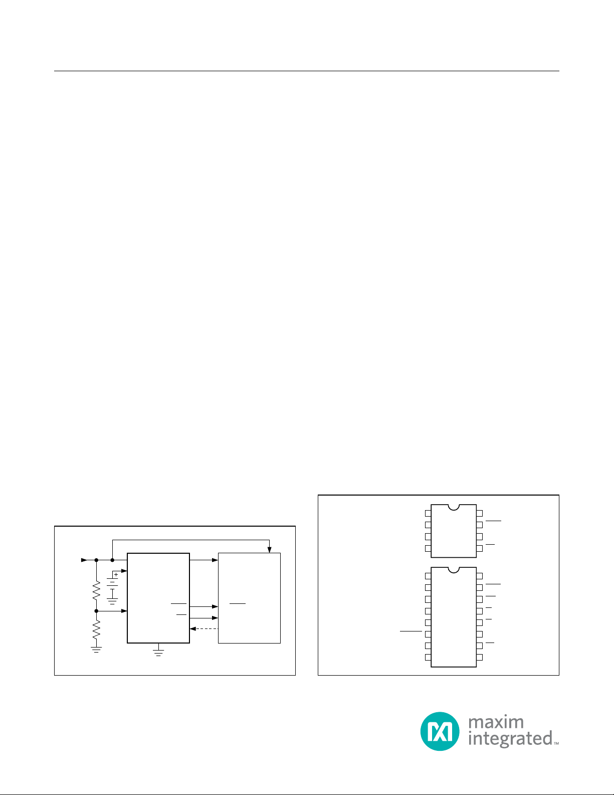
Pin Congurations
Typical Operating Circuit
+5V
19-0218; Rev 5; 4/15
V
CC
V
BATT
PFI
MAX690
GND
V
OUT
RESET
PFO
WDI
MAX690 TYPICAL APPLICATION
POWER TO
CMOS RAMµPPOWER
µP
SYSTEM
µP RESET
µP NMI
I/O
LINE
TOP VIEW
V
OUT
V
GND
V
BATT
V
OUT
V
GND
BATT ON
LOW LINE
OSC IN
81
V
161
152
143
13
125
116
10
72
63
5
98 PFIOSC SEL
BATT
RESET
WDI
PFO
RESET
RESET
WDO
CE IN
CE OUT
WDI
PFO
MAX690
CC
MAX692
MAX694
4
PFI
MAX691
CC
MAX693
4
MAX695
7
Page 2

MAX690–MAX695 Microprocessor Supervisory Circuits
Absolute Maximum Ratings
Terminal Voltage (with respect to GND)
VCC ...................................................................-0.3V to +6.0V
V
All Other Inputs (Note 1) ................... -0.3V to (V
...............................................................-0.3V to +6.0V
BATT
OUT
+ 0.5V)
Input Current
VCC ...............................................................................200mA
V
.............................................................................50mA
BATT
GND ...............................................................................20mA
Output Current
V
..................................................... Short circuit protected
OUT
All Other Outputs ............................................................20mA
Rate-of-Rise, V
BATT, VCC
..............................................100V/µs
Operating Temperature Range
C suffix ................................................................0°C to +70°C
E suffix ............................................................ -40°C to +85°C
M suffix ......................................................... -55°C to +125°C
Stresses beyond those listed under “Absolute Maximum Ratings” may cause permanent damage to the device. These are stress ratings only, and functional operation of the device at these
or any other conditions beyond those indicated in the operational sections of the specifications is not implied. Exposure to absolute maximum rating conditions for extended periods may affect
device reliability.
Electrical Characteristics
V
= full operating range, V
CC
= 2.8V, TA = +25°C, unless otherwise noted.)
BATT
Power Dissipation
8-Pin Plastic DIP
(derate 5mW/°C above +70°C) ....................................400mV
8-Pin CERDIP
(derate 8mW/°C above +85°C) ....................................500mV
16-Pin Plastic DIP
(derate 7mW/°C above +70°C) ....................................600mV
16-Pin Small Outline
(derate 7mW/°C above +70°C) ....................................600mV
16-Pin CERDIP
(derate 10mW/°C above +85°C) ..................................600mV
Storage Temperature Range ............................ -65°C to +160°C
Lead Temperature (Soldering, 10s) ................................... 300°C
PARAMETER CONDITIONS MIN TYP MAX UNITS
BATTERY BACKUP SWITCHING
Operating Voltage Range
(MAX690, MAX691, MAX694, MAX695 VCC)
Operating Voltage Range (MAX690, MAX691,
MAX694, MAX695 V
BATT
)
Operating Voltage Range
(MAX692, MAX693 VCC)
Operating Voltage Range
(MAX692, MAX693 V
V
Output Voltage
OUT
V
in Battery Backup Mode I
OUT
Supply Current (Excluded I
BATT
)
OUT
I
= 1mA
OUT
I
= 50mA
OUT
= 250µA, VCC < V
OUT
I
= 1mA 2 5
)
OUT
I
= 50mA 3.5 10
OUT
Supply Current in Battery Backup Mode VCC = 0V, V
Battery Standby Current
(+ = Discharge, - = Charge)
Battery Switchover Threshold
(VCC - V
BATT
)
5.5V > VCC >
V
+ 1V
BATT
Power-up 70
Power-down 50
4.75 5.5
2.0 4.25
4.5 5.5
2.0 4.0
VCC -
0.3
VCC -
0.5
V
- 0.2V
BATT
= 2.8V 0.6 1 µA
BATT
BATT
- 0.1
VCC -
0.1
VCC -
0.25
V
BATT
- 0.02
TA = +25°C -0.1 +0.02
TA = full operating
range
-1.0 +0.02
V
V
V
mA
µA
mV
www.maximintegrated.com
Maxim Integrated
│
2
Page 3
MAX690–MAX695 Microprocessor Supervisory Circuits
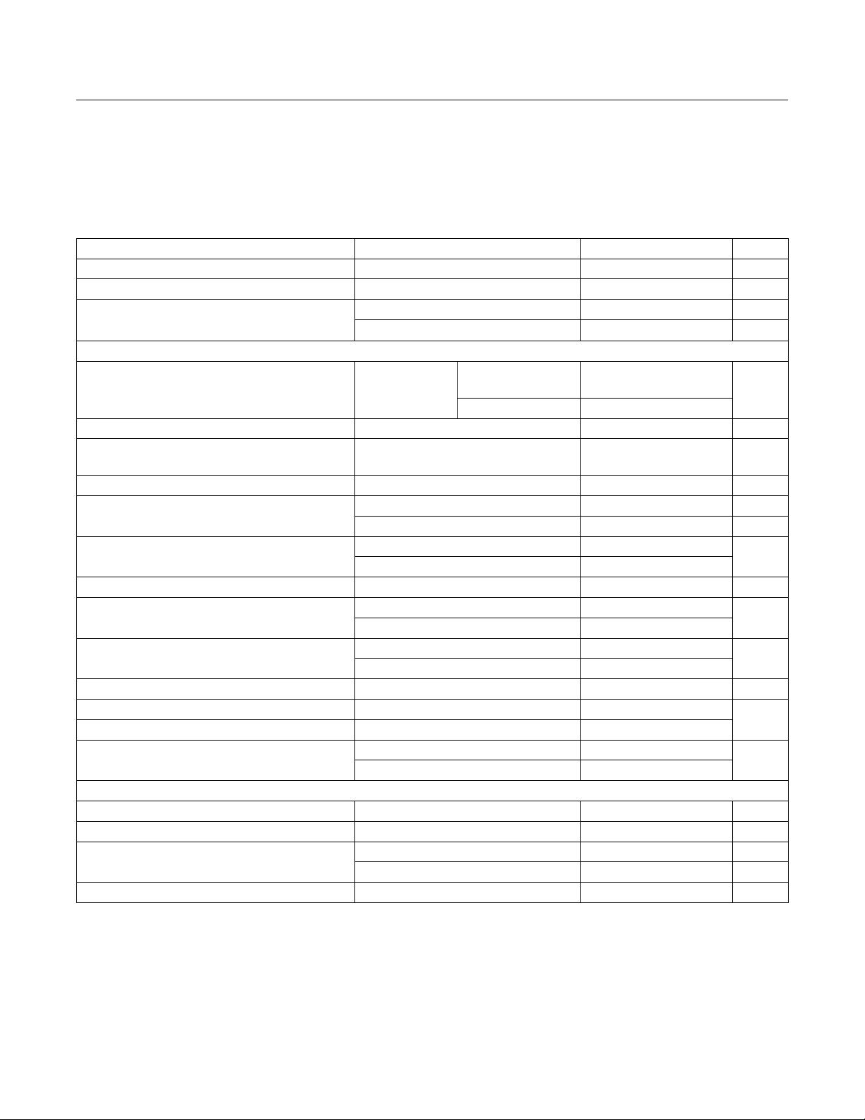
Electrical Characteristics (continued)
V
= full operating range, V
CC
PARAMETER CONDITIONS MIN TYP MAX UNITS
Battery Switchover Hysteresis 20 mV
BATT ON Output Voltage I
BATT ON Output Short-Circuit Current
RESET AND WATCHDOG TIMER
Reset Voltage Threshold
Reset Threshold Hysteresis 40 mV
Reset Timeout Delay (MAX690/MAX691/
MAX692/MAX693)
Reset Timeout Delay (MAX694/MAX695) Figure 6, OSC SEL HIGH, VCC = 5V 140 200 280 ms
Watchdog Timeout Period, Internal Oscillator
Watchdog Timeout Period, External Clock
Minimum WDI Input Pulse Width VIL = 0.4, VIH = 0.8V
RESET and LOW LINE Output Voltage
RESET and WDO Output Voltage
Output Short-Circuit Current RESET, RESET, WDO, LOW LINE 1 3 25 µA
WDI Input Threshold Logic-Low VCC = 5V (Note 2) 0.8
WDI Input Threshold Logic-High VCC = 5V (Note 2) 3.5
WDI Input Current
POWER-FAIL DETECTOR
PFI Threshold VCC = 5V, TA = full 1.2 1.3 1.4 V
PFI Current ±0.01 ±25 nA
PFO Output Voltage
PFO Short Circuit Source Current PFI = VIH, PFO = 0V 1 3 25 µA
= 2.8V, TA = +25°C, unless otherwise noted.)
BATT
= 3.2mA 0.4 V
SINK
BATT ON = V
OUT
BATT ON = 0V source current 0.5 1 25 µA
TA = full
operating range
Figure 6, OSC SEL HIGH, VCC = 5V 35 50 70 ms
Long period, VCC = 5V 1.0 1.6 2.25 s
Short period, VCC = 5V 70 100 140 ms
Long period 3840 4097
Short period 768 1025
I
= 1.6mA, VCC = 4.25V 0.4
SINK
I
SOURCE
I
SINK
I
SOURCE
WDI = V
= 1µA, VCC = 5V 3.5
= 1.6mA 0.4
= 1µA, VCC = 5V 3.5
OUT
WDI = 0V -50 -15
I
= 3.2mA 0.4 V
SINK
I
SOURCE
= 1µA 3.5 V
= 4.5V sink current 25 mA
MAX690, MAX691,
MAX694, MAX695
4.5 4.65 4.75
V
MAX692, MAX693 4.25 4.4 4.5
Clock
Cycles
CC
200 ns
V
V
V
20 50
µA
www.maximintegrated.com
Maxim Integrated
│
3
Page 4
MAX690–MAX695 Microprocessor Supervisory Circuits
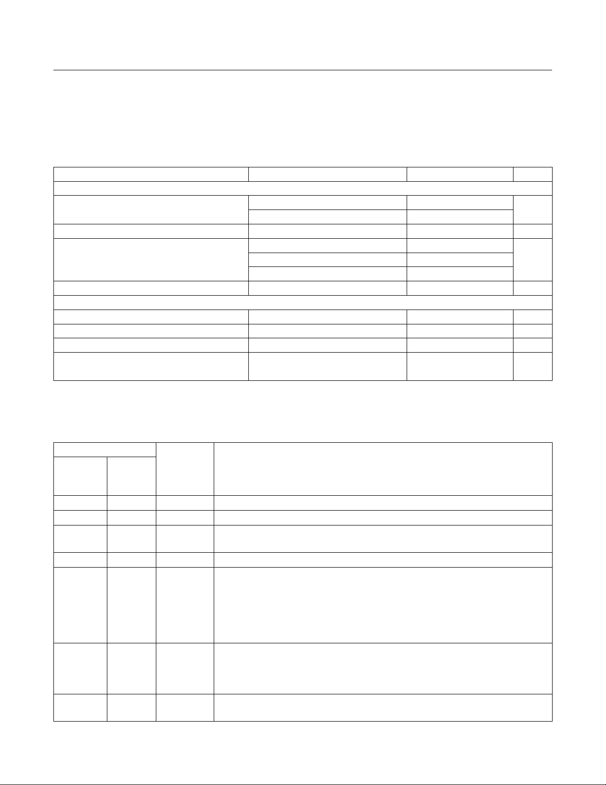
Electrical Characteristics (continued)
V
= full operating range, V
CC
PARAMETER CONDITIONS MIN TYP MAX UNITS
CHIP ENABLE GATING
CE IN Thresholds
CE IN Pullup Current 3 µA
CE OUT Output Voltage
CE Propagation Delay VCC = 5V 50 200 ns
OSCILLATOR
OSC IN Input Current ±2 µA
OSC SEL Input Pullup Current 5 µA
OSC IN Frequency Range OSC SEL = 0V 0 250 kHz
OSC IN Frequency
with External Capacitor
Note 1: The input voltage limits on PFI and WDI may be exceeded provided the input current is limited to less than 10mA.
Note 2: WDI is guaranteed to be in the mid-level (inactive) state if WDI is floating and VCC is in the operating voltage range. WDI is
internally biased to 38% of VCC with an impedance of approximately 125kΩ.
= 2.8V, TA = +25°C, unless otherwise noted.)
BATT
V
IL
V
IH
I
= 3.2mA 0.4
SINK
SOURCE
I
SOURCE
= 3.0mA V
= 1µA, VCC = 0V V
OSC SEL = 0V
C
= 47pF
OSC
3.0
OUT
OUT
- 1.5
- 0.05
4 kHz
0.8
V
VI
Pin Description
PIN
MAX690/
MAX692/
MAX694
2 3 V
8 1 V
1 2 V
3 4 GND 0V Ground Reference for All Signals
7 15 RESET
6 11 WDI
4 9 PFI
MAX691/
MAX693/
MAX695
NAME FUNCTION
CC
BATT
OUT
The +5V Input
Backup Battery Input. Connect to Ground if a backup battery is not used.
The higher of VCC or V
V
OUT
and V
are not used. Connect a 0.1µF or larger bypass capacitor to V
BATT
RESET goes low whenever VCC falls below either the reset voltage threshold or the
V
input voltage. The reset threshold is typically 4.65V for the MAX690/691/694/695,
BATT
and 4.4V for the MAX692 and MAX693. RESET remains low for 50ms after VCC returns
to 5V, (except 200ms in MAX694/695). RESET also goes low for 50ms if the Watchdog
Timer is enabled but not serviced within its timeout period. The RESET pulse width can
be adjusted as shown in Table 1.
Watchdog Input (WDI). WDI is a three level input. If WDI remains either high or low for
longer than the watchdog timeout period, RESET pulses low and WDO goes low. The
Watchdog Timer is disabled when WDI is left oating or is driven to mid-supply. The
timer resets with each transition at the Watchdog Timer input.
Noninverting Input to the Power-Fail Comparator. When PFI is less than 1.3V, PFO
goes low. Connect PFI to GND or V
is internally switched to V
BATT
when not used. See Figure 1.
OUT
. Connect V
OUT
OUT
to VCC if
OUT
.
www.maximintegrated.com
Maxim Integrated
│
4
Page 5

MAX690–MAX695 Microprocessor Supervisory Circuits
Pin Description (continued)
PIN
MAX690/
MAX692/
MAX694
5 10 PFO
— 13 CE IN CE Gating Circuit Input. Connect to GND or V
— 12 CE OUT
MAX691/
MAX693/
MAX695
NAME FUNCTION
Output of the Power-Fail Comparator. It goes low when PFI is less than 1.3V. The
comparator is turned off and PFO goes low when VCC is below V
OUT
CE OUT goes low only when CE IN is low and VCC is above the reset threshold (4.65V
for MAX691 and MAX695, 4.4V for MAX693). See Figure 6.
if not used.
BATT
.
BATT ON goes high when V
— 5 BATT ON
— 6 LOW LINE
— 16 RESET Active-High Output. It is the inverse of RESET.
— 8 OSC SEL
— 7 OSC IN
— 14 WDO
when V
directly drive the base of an external PNP transistor to increase the output current
above the 50mA rating of V
LOW LINE goes low when VCC falls below the reset threshold. It returns high as soon
as VCC rises above the reset threshold. See Figure 6, Reset Timing.
When OSC SEL is unconnected or driven high, the internal oscillator sets the reset time
delay and watchdog timeout period. When OSC SEL is low, the external oscillator input,
OSC IN, is enabled. OSC SEL has a 3µA internal pullup. See Table 1.
When OSC SEL is low, OSC IN can be driven by an external clock to adjust both the
reset delay and the watchdog timeout period. The timing can also be adjusted by
connecting and external oscillator to this pin. See Figure 8. When OSC SEL is high or
oating, OSC IN selects between fast and slow Watchdog timeout periods.
The Watchdog Output (WDO). WDO goes low if WDI remains either high or low for
longer than the watchdog timeout period. WDO is set high by the next transition at WDI.
If WDI is unconnected or at mid-supply, WDO remains high. WDO also goes high when
LOW LINE goes low.
is internally switched to VCC. The output typically sinks 25mA and can
OUT
is internally switched to the V
OUT
.
OUT
input. It goes low
BATT
www.maximintegrated.com
Maxim Integrated
│
5
Page 6
MAX690–MAX695 Microprocessor Supervisory Circuits
Typical Applications
MAX691, MAX693, and MAX695
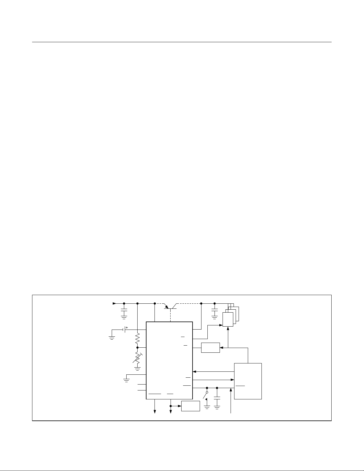
A typical connection for the MAX691/693/695 is shown
in Figure 1. CMOS RAM is powered from V
internally connected to VCC when 5V power is present,
or to V
V
OUT
when VCC is less than the battery voltage.
BATT
can supply 50mA from VCC, but if more current
is required, an external PNP transistor can be added.
When VCC is higher than V
, the BATT ON output
BATT
goes low, providing 25mA of base drive for the external
transistor. When VCC is lower than V
BATT
200Ω MOSFET connects the backup battery to V
The quiescent current in the battery backup mode is 1µA
maximum when VCC is between 0V and V
Reset Output
A voltage detector monitors VCC and generates a RESET
output to hold the microprocessor’s Reset line low when
VCC is below 4.65V (4.4V for MAX693). An internal
monostable holds RESET low for 50ms* after VCC rises
above 4.65V (4.4V for MAX693). This prevents repeated
toggling of RESET even if the 5V power drops out and
recovers with each power line cycle.
The crystal oscillator normally used to generate the clock
for microprocessors takes several milliseconds to start.
Since most microprocessors need several clock cycles
to reset, RESET must be held low until the microprocessor clock oscillator has started. The MAX690 family
*200ms for MAX695
. V
OUT
OUT
, an internal
OUT
–700mV.
BATT
is
.
power-up RESET pulse lasts 50ms* to allow for this
oscillator start-up time. The manual reset switch and
the 0.1µF capacitor connected to the reset bus can be
omitted if manual reset is not needed. An inverted, active
high, RESET output is also supplied.
Power-Fail Detector
The MAX691/93/95 issues a nonmaskable interrupt (NMI)
to the microprocessor when a power failure occurs. The
+5V power line is monitored via two external resistors
connected to the power-fail input (PFI). When the voltage at PFI falls below 1.3V, the power-fail output (PFO)
drives the processor’s NMI input low. If a power-fail
threshold of 4.8V is chosen, the microprocessor will
have the time when VCC fails from 4.8V to 4.65V to save
data into RAM. An earlier power-fail warning can be
generated if the unregulated DC input of the 5V regulator
is available for monitoring.
RAM Write Protection
The MAX691/MAX693/MAX695 CE OUT line drives the
Chip Select inputs of the CMOS RAM. CE OUT follows
CE IN as long as VCC is above the 4.65V (4.4V for
MAX693) reset threshold. If VCC falls below the reset
threshold, CE OUT goes high, independent of the logic
level at CE IN. This prevents the microprocessor from
writing erroneous data into RAM during power-up, powerdown, brownouts, and momentary power interruptions.
The LOW LINE output goes low when VCC falls below
4.65V (4.4V for MAX693).
+5V
V
CC
INPUT
0.1µF
3V
BATTERY
NO CONNECTION
Figure 1. MAX691/693/695 Typical Application
www.maximintegrated.com
5
3
BATT ON
V
CC
1
V
BATT
9
PFI
MAX691
MAX693
MAX695
4
GND
7
OSC IN
8
OSC SEL
LOW LINE WDO
6 14
SYSTEM STATUS INDICATORS
V
OUT
CE OUT
CE IN
WDI
PFO
RESET
AUDIBLE
ALARM
0.1µF
2
12
13
ADDRESS
DECODE
11
10
15
RESET
OTHER SYSTEM RESET SOURCES
0.1µF
CMOS
RAM
A0-A15
I/O
NMI
RESET
MICROPROCESSOR
Maxim Integrated
│
6
Page 7
MAX690–MAX695 Microprocessor Supervisory Circuits
Watchdog Timer
The microprocessor drives the WATCHDOG INPUT
(WDI) with an I/O line. When OSC IN and OSC SEL are
unconnected, the microprocessor must toggle the WDI
pin once every 1.6s to verify proper software execution. If
a hardware or software failure occurs such that WDI not
toggled the MAX691/MAX693 will issue a 50ms* RESET
pulse after 1.6s. This typically restarts the microprocessor’s power-up routine. A new RESET pulse is issued
every 1.6s until the WDI is again strobed.
The WATCHDOG OUTPUT (WDO) goes low if the
watchdog timer is not serviced within its timeout period.
Once WDO goes low it remains low until a transition
occurs at WDI. The watchdog timer feature can be disabled by leaving WDI unconnected. OSC IN and OSC
SEL also allow other watchdog timing options, as shown
in Table 1 and Figure 8.
MAX690, MAX692, and MAX694
The 8 pin MAX690, MAX692, and MAX694 have most
of the features of the MAX691, MAX693, and MAX695.
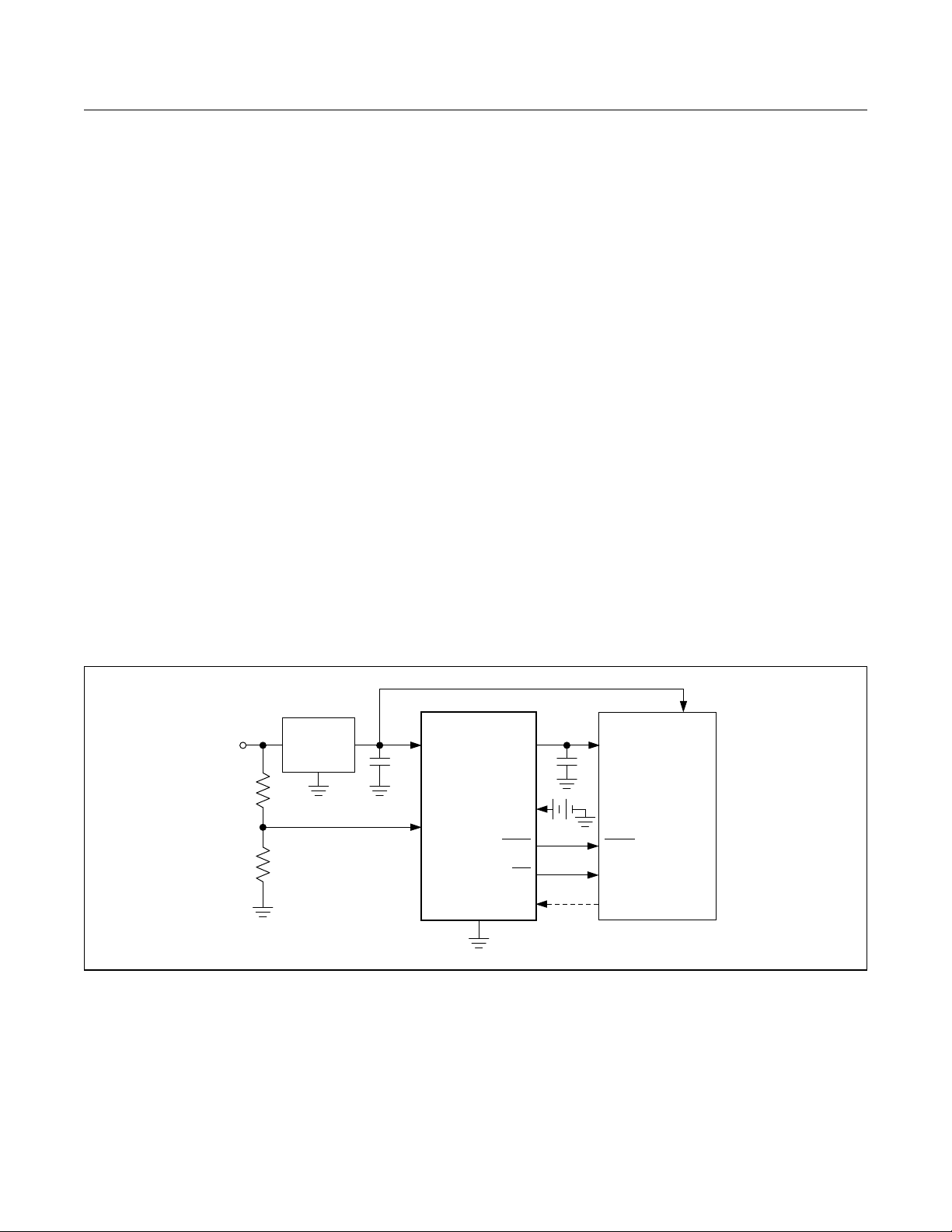
Figure 2 shows the MAX690/MAX692/MAX694 in a typical
*200ms for MAX695
application. Operation is much the same as with the
MAX691/MAX693/MAX695 (Figure 1), but in this case, the
power- fail input (PFI) monitors the unregulated input to the
7805 regulator. The MAX690/MAX694 RESET output goes
low when VCC falls below 4.65V. The RESET output of the
MAX692 goes low when VCC drops below 4.4V.
The current consumption of the battery-backed-up power
bus must be less than 50mA. The MAX690/MAX692/
MAX694 does not have a BATT ON output to drive an
external transistor. The MAX690/MAX692/MAX694 also
does not include chip enable gating circuitry that is available on the MAX690/MAX692/MAX694. In many systems
though, CE gating is not needed since a low input to
the microprocessor RESET line prevents the processor
from writing to RAM during power-up and power-down
transients.
The MAX690/MAX692/MAX694 watchdog timer has a
fixed 1.6s timeout period. If WDI remains either low or
high for more than 1.6s, a RESET pulse is sent to the
microprocessor. The watchdog timer is disabled if WDI is
left unconnected.
+8V +5V
7805
3-TERMINAL
REGULATOR
Figure 2. MAX690/692/694 Typical Application
0.1µF
POWER
2
V
CC
MAX690
MAX692
MAX694
4
PFI
GND
V
OUT
V
BATT
RESET
PFO
WDI
3
0.1µF
1
8
7
5
6
TO
CMOS
RAM
MICROPROCESSOR
RESET
NMI
I/O LINE
MICRO-
PROCESSOR
POWER
www.maximintegrated.com
Maxim Integrated
│
7
Page 8
MAX690–MAX695 Microprocessor Supervisory Circuits
Detailed Description
Battery-Switchover and V
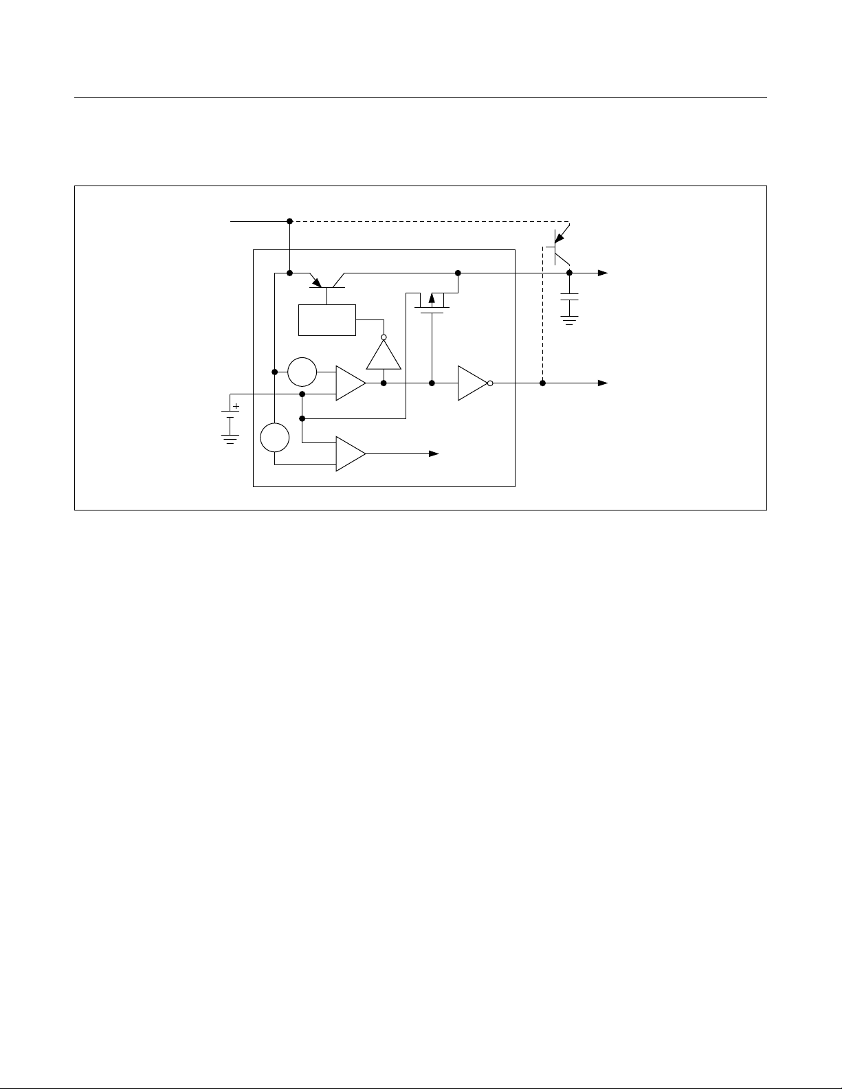
The battery switchover circuit compares VCC to the V
input, and connects V
occurs when VCC is 50mV greater than V
and VCC is 70mV more than V
Figure 4). The switchover comparator has 20mV of hysteresis to prevent repeated, rapid switching if VCC falls very
slowly or remains nearly equal to the battery voltage.
When VCC is higher than V
switched to V
tor. V
has 50mA output current capability. Use an
OUT
external PNP pass transistor in parallel with internal transistor if the output current requirement at V
50mA or if a lower VCC-V
desired. The BATT ON output (MAX691/MAX693/MAX695
only) can directly drive the base of the external transistor.
It should be noted that the MAX690–MAX695 need only
supply the average current drawn by the CMOS RAM if
there is adequate filtering. Many RAM data sheets specify
a 75mA maximum supply current, but this peak current
spike lasts only 100ns. A 0.1µF bypass capacitor at V
supplies the high instantaneous current, while V
only supply the average load current, which is much less.
A capacitance of 0.1µF or greater must be connected to
the V
terminal to ensure stability.
OUT
A 200Ω MOSFET connects V
battery backup. This MOSFET has very low input-tooutput differential (dropout voltage) at the low current
OUT
via a low saturation PNP transis-
OUT
OUT
to whichever is higher. Switchover
BATT
as VCC falls,
BATT
as V
BATT
, VCC is internally
BATT
voltage differential is
OUT
input to V
BATT
rises (see
CC
exceeds
OUT
OUT
OUT
OUT
need
during
levels required for battery backup of CMOS RAM or other
low power CMOS circuitry. When VCC equals V
supply current is typically 12µA. When VCC is between
0V and (V
- 700mV) the typical supply current is only
BATT
600nA typical, 1µA maximum.
The MAX690/MAX691/MAX694/MAX695 operate with
battery voltages from 2.0V to 4.25V while MAX692/
MAX693 operate with battery voltages from 2.0V to
4.0V. High value capacitors can also be used for shortterm memory backup. External circuitry is required to
ensure that the capacitor voltage does not rise above
the reset threshold, and that the charging resistor does
not discharge the capacitor when in backup mode. The
MAX691A and the MAX791 provide solutions requiring
fewer external components.
A small charging current of typically 10nA (0.1µA max)
flows out of the V
amount of current that is drawn from V
terminal. This current varies with the
BATT
but its polarity
OUT
is such that the backup battery is always slightly charged,
and is never discharged while VCC is in its operating voltage range. This extends the shelf life of the backup battery
by compensating for its self-discharge current. Also note
that this current poses no problem when lithium batteries
are used for backup since the maximum charging current
(0.1µA) is safe for even the smallest lithium cells.
If the battery-switchover section is not used, connect
V
to GND and connect V
BATT
to VCC. Table 2 shows
OUT
the state of the inputs and output in the low power battery
backup mode.
BATT
the
V
BATT
3
V
CC
*4.4V (MAX693)
OSC IN
INPUT
13
*
4.65V
7
8
11
9
1.3V
CHIP-ENABLE INPUT
OSC SEL
WATCHDOG INPUT
POWER FAIL
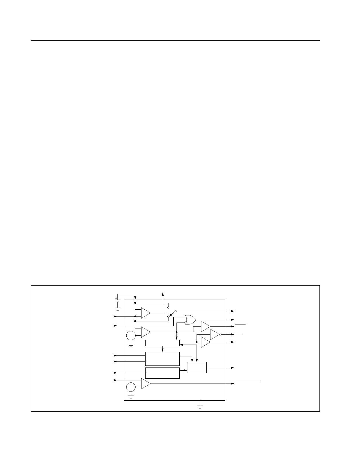
Figure 3. MAX691/MAX693/MAX695 Block Diagram
www.maximintegrated.com
+
-
+
-
RESET GENERATOR
TIMEBASE FOR RESET
AND
WATCHDOG
WATCHDOG TRANSITION
DETECTOR
+
-
BATT ON1 5
2
V
OUT
12
CHIP ENABLE OUTPUT
6
LOW LINE
15
RESET
16
RESET
WATCHDOG
TIMER
4
GROUND
14
WATCHDOG OUTPUT
10
POWER FAIL OUTPUT
Maxim Integrated
│
8
Page 9
MAX690–MAX695 Microprocessor Supervisory Circuits
V
CC
+5V
TO CMOS
RAM AND
0.1F
REALTIME
CLOCK
IN
V
CC
V
CC
BASE DRIVE
P CHANNEL
MOSFET
V
OUT
3V
BATTERY
INPUT
700
mV
100
mV
-
+
+
-
+
-
LOW IQ MODE
SELECT
Figure 4. Battery-Switchover Block Diagram
Reset Output
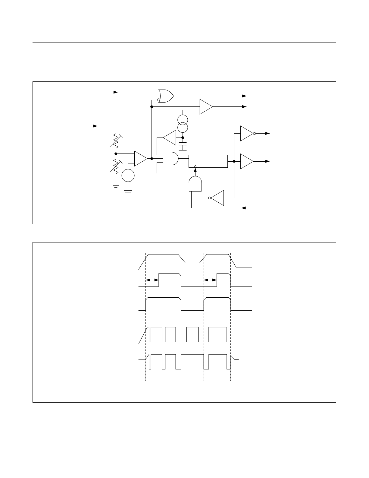
RESET is an active-low output which goes low whenever VCC falls below 4.5V (MAX690/MAX691/MAX694/
MAX695) or 4.25V (MAX692/MAX693). It will remain low
until VCC rises above 4.75V (MAX690/691/694/695) or 4.5V
(MAX692/MAX693) for milliseconds*. See Figures 5 and 6.
The guaranteed minimum and maximum thresholds of
MAX690/MAX691/MAX694/MAX695 are 4.5V and 4.75V,
while the guaranteed thresholds of the MAX692/MAX693
are 4.25V and 4.5V. The MAX690/MAX691/MAX694/
MAX695 is compatible with 5V supplies with a +10%, -5%
tolerance while the MAX692/MAX693 is compatible with
5V ±10% supplies. The reset threshold comparator has
approximately 50mV of hysteresis, with a nominal threshold of 4.65V in the MAX690/MAX691/MAX694/MAX695,
and 4.4V in the MAX692/MAX693.
The response time of the reset voltage comparator is
about 100µs. VCC should be bypassed to ensure that
glitches do not activate the RESET output.
RESET also goes low if the watchdog timer is enabled
and WDI remains either high or low longer than the watchdog timeout period. RESET has an internal 3µA pullup,
and can either connect to and open collector Reset bus
or directly drive a CMOS gate without and external pullup
resistor.
BATT ON
(MAX691, MAX693, MAX695 ONLY)
INTERNAL
SHUTDOWN
SIGNAL WHEN
V
> VCC + 0.7V
BATT
CE Gating and RAM Write Protection
The MAX691/MAX693/MAX695 use two pins to control
the Chip Enable or Write inputs of CMOS RAMs. When
VCC is +5V, CE OUT is a buffered replica of CE IN, with
a 50ns propagation delay. If VCC input falls below 4.65V
(4.5V min, 4.75V max) an internal gate forces CE OUT
high, independent of CE IN. The MAX693 CE OUT goes
high whenever VCC is below 4.4V (4.25V min, 4.5V max).
The CE output of both devices is also forced high when
VCC is less than V
CE OUT typically drives the CE, CS, or Write input of
battery backed up CMOS RAM. This ensures the integrity of the data in memory by preventing write operations
when VCC is at and invalid level. Similar protection of
EEPROMs can be achieved by using the CE OUT to
drive the Store or Write inputs of an EEPROM, EAROM,
or NOVRAM.
If the 50ns typical propagation delay of CE OUT is too
long, connect CE IN to GND and use the resulting CE
OUT to control a high speed external logic gate. A second
alternative is to AND the LOW LINE output with the CE or
WR signal. An external logic gate and the RESET output
of the MAX690/MAX692/MAX694 can also be used for
CMOS RAM write protection.
. (See Figure 5.)
BATT
*200ms for MAX694 and MAX695
www.maximintegrated.com
Maxim Integrated
│
9
Page 10
MAX690–MAX695 Microprocessor Supervisory Circuits
V
CC
METAL
TRIMMED
RESISTORS
Figure 5. Reset Block Diagram
CE IN
LINK
1.3V
CE OUT
LOW LINE
POWER-ON
RESET
+
-
WATCHDOG
FROM
WATCHDOG
TIMER
V
CC
4.7V
RESET RESET
TIME
4.7V4.6V 4.6V
Q
R
10 kHz CLOCK
FROM TIMEBASE
SECTION
RESET
RESET
Figure 6. Reset Timing
RESET
OUTPUT
LOW LINE
OUTPUT
CE
IN
CE
IN
*200ms FOR MAX694 AND MAX695
50ms*
50ms*
- V
V
OUT
BATT
www.maximintegrated.com
Maxim Integrated
│
10
Page 11
MAX690–MAX695 Microprocessor Supervisory Circuits
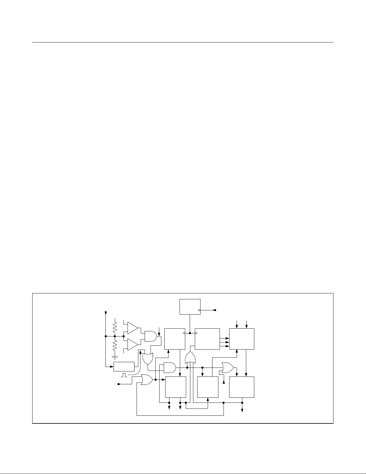
1.3V Comparator and Power-Fail Warning
The power-fail input (PFI) is compared to an internal
1.3V reference. The power-fail output (PFO) goes low
when the voltage at PFI is less than 1.3V. Typically, PFI is
driven by an external voltage divider which senses either
the unregulated DC input to the system’s 5V regulator or
the regulated 5V output. The voltage divider ratio can be
chosen such that the voltage at PFI falls below 1.3V several milliseconds before the +5V supply falls below 4.75V.
PFO is normally used to interrupt the microprocessor so
that data can be stored in RAM before VCC falls below
4.75V and the RESET output goes low (4.5V for MAX692/
MAX693).
The power-fail detector can also monitor the backup battery to warn of a low battery condition. To conserve battery power, the power-fail detector comparator is turned
off and PFO is forced when VCC is lower than V
BATT
input voltage.
Watchdog Timer and Oscillator
The watchdog circuit monitors the activity of the microprocessor. If the microprocessor does not toggle the
Watchdog Input (WDI) within the selected timeout period,
a 50ms* RESET pulse is generated. Since many systems
cannot service the watchdog timer immediately after a
reset, the MAX691/MAX693/MAX695 has a longer timeout period after reset is issued. The normal timeout period
becomes effective following the first transition of WDI after
RESET has gone high. The watchdog timer is restarted
at the end of reset, whether the reset was caused by
lack of activity on WDI or by VCC falling below the reset
threshold. If WDI remains either high or low, reset pulses
will be issued every 1.6s. The watchdog monitor can be
deactivated by floating the watchdog input (WDI).
The watchdog output (WDO, MAX691/MAX693/MAX695
only) goes low if the watchdog timer times out and
remains low until set high by the next transition on the
watchdog input. WDO is also set high when VCC goes
below the reset threshold.
The watchdog timeout period is fixed at 1.6s and the
reset pulse width is fixed at 50ms* on the 8-pin MAX690/
MAX692/MAX694. The MAX691/MAX693/MAX695 allow
these times to be adjusted per Table 1.
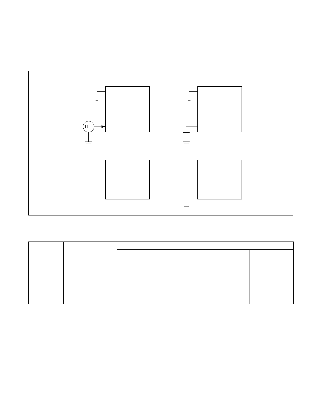
Figures 8 shows
various oscillator configurations.
The internal oscillator is enabled when OSC SEL is
floating. In this mode, OSC IN selects between the
1.6s and 100ms watchdog timeout periods. In either
case, immediately after a reset the timeout period 1.6s.
This gives the microprocessors time to reintialize the
system. If OSC IN is low, then the 100ms watchdog
period becomes effective after the first transition of WDI.
The software should be written such that the I/O port
driving WDI is left in its power-up reset state until the initialization routines are completed and the microprocessor
is able to toggle WDI at the minimum watchdog timeout
period of 70ms.
*200ms for MAX694
WATCHDOG INPUT
V
CC
2.7V
1.0V
TRANSACTION
DETECTOR
FOR EACH TRANSITION
LOW LINE
(HI IF V
< 4.65V)
CC
Figure 7. Watchdog Timer Block Diagram
www.maximintegrated.com
PRESCALER
+
-
-
+
HI IF WATCHDOG
INPUT IS FLOATING
RESET RESET
RESET
COUNTER
R Q10/12
S R
RESET
FLIP FLOP
Q
Q
10.24 kHz FROM INTERNAL OSCILLATOR
OR EXTERNALLY SET FREQUENCY FROM
Q6
WATCHDOG
COUNTER
R
S R
LONG/SHORT
OSC IN PIN
WATCHDOG TIMEOUT SELECT
Q11
Q13
Q15
Q
LOW
FF
LINE
R
WATCHDOG
TIMEOUT
SELECTOR
LOGIC
GOES HIGH AT THE
END OF WATCHDOG
TIMEOUT PERIOD
S
WATCHDOG
FAULT FF
Q
WATCHDOG OUTPUT
Maxim Integrated
│
11
Page 12
C(pF)
MAX690–MAX695 Microprocessor Supervisory Circuits
Figure 8. Oscillator Circuits
0 TO 250kHz
N.C.
N.C.
EXTERNAL CLOCK
8
OSC SEL
MAX691
MAX693
MAX695
7
OSC IN
INTERNAL OSCILLATOR
1.6s WATCHDOG
8
OSC SEL
MAX691
MAX693
MAX695
7
OSC IN
EXTERNAL OSCILLATOR
8
OSC SEL
MAX691
MAX693
MAX695
7
OSC IN
C
OSC
INTERNAL OSCILLATOR
100ms WATCHDOG
8
N.C.
OSC SEL
MAX691
MAX693
MAX695
7
OSC IN
Table 1. MAX691/MAX693/MAX695 Reset Pulse Width and Watchdog Timeout Selections
WATCHDOG TIMEOUT PERIOD RESET TIMEOUT PERIOD
OSC SEL OSC IN
NORMAL
Low External Clock Input 1024 clks 4096 clks 512 clks 2048 clks
Low External Capacitor 400ms/47pF x C 1.6s/47pF x C 200ms/47pF x C 800ms/47pF x C
Floating Low 100ms 1.6s 50ms 200ms
Floating Floating 1.6s 1.6s 50ms 200ms
Note 1: The MAX690/MAX692/MAX694 watchdog timeout period is fixed at 1.6s nominal, the MAX690/692 reset pulse width is fixed
at 50ms nominal and the MAX694 is 200ms nominal.
Note 2: When the MAX691 OSC SEL pin is low, OSC IN can be driven by an external clock signal or an external capacitor can be
connected between OSC IN and GND. The nominal internal oscillator frequency is 6.55kHz. The nominal oscillator frequency
with capacitor is:
f (Hz)
OSC
Note 3: See Electrical Characteristics table for minimum and maximum timing values.
IMMEDIATELY
AFTER REST
120,000
=
MAX691/MAX693 MAX695
www.maximintegrated.com
Maxim Integrated
│
12
Page 13
MAX690–MAX695 Microprocessor Supervisory Circuits
Application Hints
Other Uses of the Power-Fail Detector
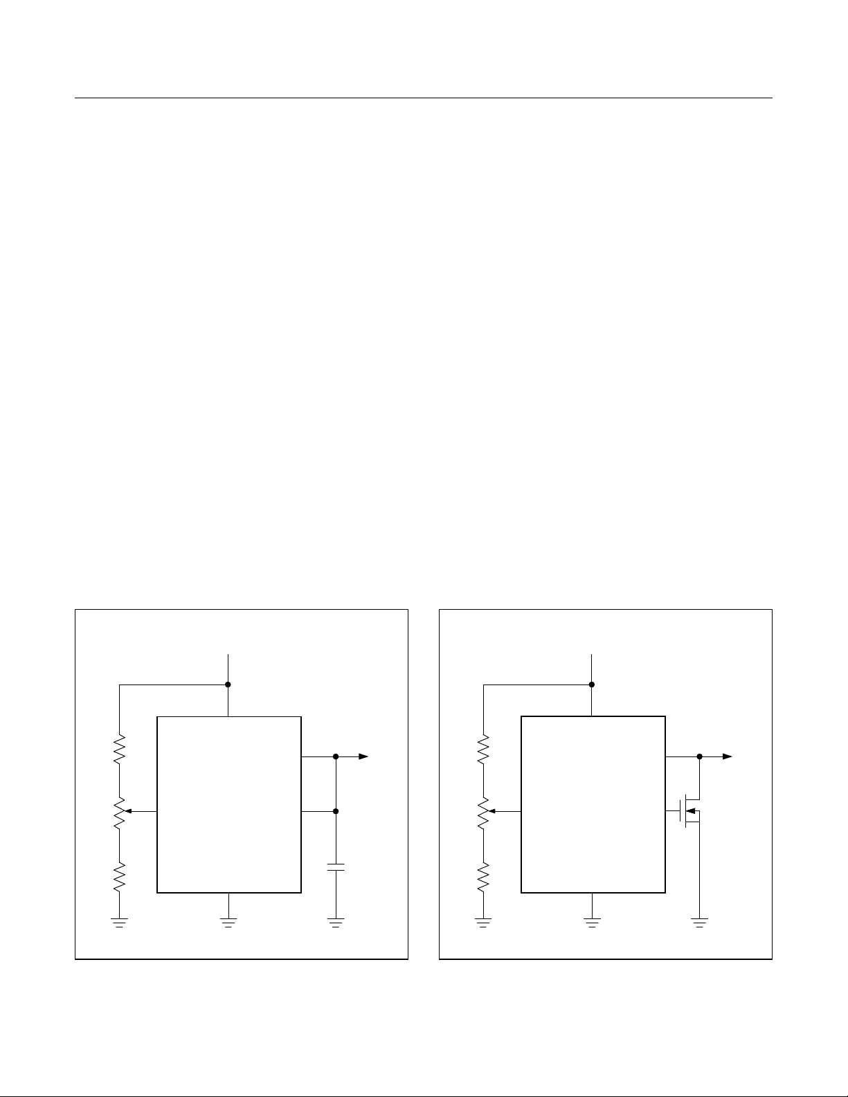
In Figure 9, the power-fail detector is used to initiate a
system reset when VCC falls to 4.85V. Since the threshold of the power-fail detector is not as accurate as the
onboard reset-voltage detector, a trimpot must be used
to adjust the voltage detection threshold. Both the PFO
and RESET outputs have high sink current capability and
only 10µA of source current drive. This allows the two
outputs to be connected directly to each other in a wired
OR fashion.
The overvoltage detector circuit in Figure 10 resets the
microprocessor whenever the nominal 5V VCC is above
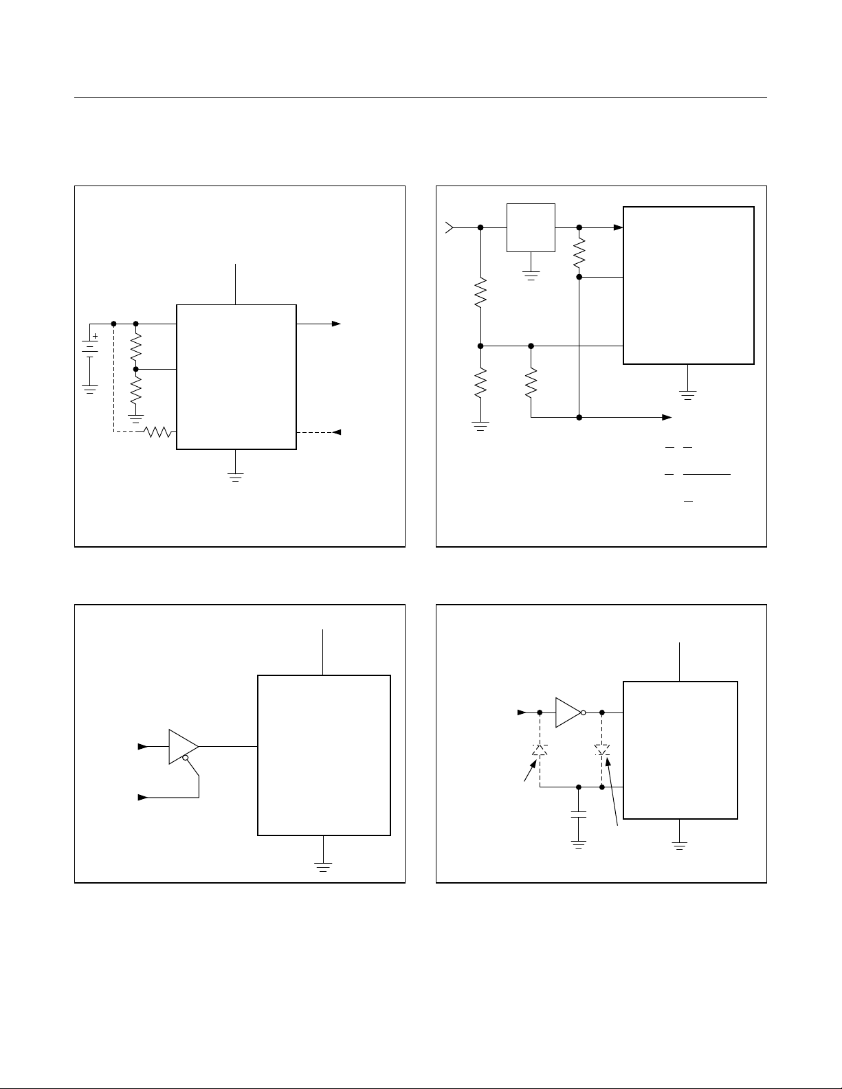
5.5V. The battery monitor circuit (Figure 11) shows the
status of the memory backup battery. If desired, the CE
OUT can be used to apply a test load to the battery. Since
CE OUT is forced high during the battery backup mode,
the test load will not be applied to the battery while it is in
use even if the microprocessor is not powered.
Adding Hysteresis
to the Power Fail Comparator
Since the power fail comparator circuit is noninverting, hysteresis can be added by connecting a resistor
between the PFO output and the PFI input as shown in
Figure 12. When PFO is low, resistor R3 sinks current
from the summing junction at the PFI pin. When PFO is
high, the series combination of R3 and R4 source current
into the PFI summing junction.
Alternate Watchdog Input Drive Circuits
The Watchdog feature can be enabled and disabled
under program control by driving WDI with a three-state
buffer (Figure 13). The drawback to this circuit is that a
software fault may be erroneously three-state the buffer,
thereby preventing the MAX690 from detecting that the
microprocessor is no longer working. In most cases a better method is to extend the watchdog period rather than
disabling the watchdog. See Figure 14. When the control
input is high, the OSC SEL pin is low and the watchdog
timeout is set by the external capacitor. A 0.01µF capacitor sets a watchdog timeout delay of 100s. When the
control input is low the OSC SEL pin is high, selecting
the internal oscillator. The 100ms or the 1.6s period is
chosen, depending on which diode in Figure 14 is used.
29.4kΩ
2kΩ
10kΩ
PFI
+5V
V
CC
MAX690
MAX691
MAX692
MAX693
MAX694
MAX695
GND
RESET
PFO
TO µP
RESET
INPUT
35.7kΩ
2kΩ
10kΩ
PFI
+5V
V
CC
MAX690
MAX691
MAX692
MAX693
MAX694
MAX695
GND
RESET
PFO
Figure 9. Externally Adjustable VCC Reset Threshold Figure 10. Reset on Overvoltage or Undervoltage
TO µP
RESET
INPUT
N-CHANNEL
www.maximintegrated.com
Maxim Integrated
│
13
Page 14
MAX690–MAX695 Microprocessor Supervisory Circuits
+5V
10MΩ
10MΩ
V
PFI
BATT
V
CC
MAX690
MAX691
MAX692
MAX693
MAX694
PFO
LOW BATTERY
SIGNAL TO
µP I/O PIN
MAX695
LOW
LOAD
FROM µP
I/O PIN
CE OUT
R
L
GND
CE IN
APPLIES
TO BATTERY
Figure 11. Backup VBattery Monitor with Optional Test Load
7805
+5V7V TO 15V
R1
75kΩ
R4
10kΩ
V
PFO
CC
MAX690
MAX691
MAX692
MAX693
MAX694
MAX695
R2
13kΩ
= 9.125V
V
H
VL = 7.9V
HYSTERESIS = 1.23V
R3
300kΩ
PFI
V
= 1.3V (1 + +
H
VL = 1.3V (1 + -
HYSTERESIS 5V x
ASSUMING R4 < < R3
GND
TO P
R1R2R1
)
R3
R1R2(5V -1.3V) R1
1.3V (R3 + R4)
R1
R3
Figure 12. Adding Hysteresis to the Power-Fail Voltage
Comparator
)
+5V
V
CC
MAX690
WATCHDOG
STROBE
EN
WDI
MAX691
MAX692
MAX693
MAX694
WATCHDOG
DISABLE
MAX695
GND
Figure 13. Disabling the Watchdog Under Program Control
+5V
V
LOW = INTERNAL
WATCHDOG TIMEOUT
HI = EXTERNAL
WATCHDOG
TIMEOUE
CONNECT FOR
100ms TIMEOUT
WHEN INTERNAL
TIMEOUT IS
SELECTED
OSC SEL
OSC IN
CONNECT FOR
1.6s INTERNAL
TIMEOUT
CC
MAX691
MAX693
GND
Figure 14. Selecting Internal or External Watchdog Timeout
www.maximintegrated.com
Maxim Integrated
│
14
Page 15

MAX690–MAX695 Microprocessor Supervisory Circuits
Table 2. Input and Output Status In Battery Backup Mode
V
, V
BATT
OUT
RESET Logic-low
RESET Logic-high. The open circuit output voltage is equal to V
LOW LINE Logic-low
BATT ON Logic-high
WDI
WDO Logic-high
PFI The power-fail comparator is turned off and the power-fail input voltage has no effect on the power-fail output.
PFO Logic-low
CE IN
CE OUT Logic-high
OSC IN OSC IN is ignored.
OSC SEL OSC SEL is ignored.
V
CC
V
is connected to V
BATT
via internal MOSFET.
OUT
OUT
.
WDI is internally disconnected from its internal pullup and does not source or sink current as long as its input
voltage is between GND and V
. The input voltage does not affect the source current.
OUT
CE IN is internally disconnected from its internal pullup and does not source or sink current as long as its input
voltage is between GND and V
Approximately 12µA is drawn from the V
The supply current is 1µA maximum when VCC is less than V
. The input voltage does not affect the source current.
OUT
input when VCC is between V
BATT
BATT
- 700mV.
BATT
+100mV and V
BATT
- 700mV.
www.maximintegrated.com
Maxim Integrated
│
15
Page 16

MAX690–MAX695 Microprocessor Supervisory Circuits
Ordering Information
PART TEMP RANGE PIN-PACKAGE
MAX690CPA 0°C to +70°C 8 Lead Plastic DIP
MAX690C/D 0°C to +70°C Dice*
MAX690EPA -40°C to +85°C 8 Lead Plastic DIP
MAX690EJA -40°C to +85°C 8 Lead CERDIP
MAX690MJA -55°C to +125°C 8 Lead CERDIP
MAX691CPE 0°C to +70°C 16 Lead Plastic DIP
MAX691CWE 0°C to +70°C 16 Lead Wide SO
MAX691C/D 0°C to +70°C Dice*
MAX691EPE -40°C to +85°C 16 Lead Plastic DIP
MAX691EWE -40°C to +85°C 16 Lead Wide SO
MAX691EJE -40°C to +85°C 16 Lead CERDIP
MAX691MJE -55°C to +125°C 16 Lead CERDIP
MAX692C/D 0°C to +70°C Dice
MAX692CPA 0°C to +70°C 8 Lead Plastic DIP
MAX692EPA -40°C to +85°C 8 Lead Plastic DIP
MAX692EJA -40°C to +85°C 8 Lead CERDIP
MAX692MJA -55°C to +125°C 8 Lead CERDIP
MAX693C/D 0°C to +70°C Dice
*Contact factory for dice specifications.
Devices in PDIP and SO packages are available in both leaded and lead-free packaging. Specify lead free by adding the + symbol at
the end of the part number when ordering. Lead free not available for CERDIP package.
PART TEMP RANGE PIN-PACKAGE
MAX693CPE 0°C to +70°C 16 Lead Plastic DIP
MAX693CWE 0°C to +70°C 16 Lead Wide SO
MAX693EPE -40°C to +85°C 16 Lead Plastic DIP
MAX693EJE -40°C to +85°C 16 Lead CERDIP
MAX693EWE -40°C to +85°C 16 Lead Wide SO
MAX693MJE -55°C to +125°C 16 Lead CERDIP
MAX694C/D 0°C to +70°C Dice
MAX694CPA 0°C to +70°C 8 Lead Plastic DIP
MAX694EPA -40°C to +85°C 8 Lead Plastic DIP
MAX694EJA -40°C to +85°C 8 Lead CERDIP
MAX694MJA -55°C to +125°C 8 Lead CERDIP
MAX695C/D 0°C to +70°C Dice
MAX695CPE 0°C to +70°C 16 Lead Plastic DIP
MAX695CWE 0°C to +70°C 16 Lead Wide SO
MAX695EPE -40°C to +85°C 16 Lead Plastic DIP
MAX695EJE -40°C to +85°C 16 Lead CERDIP
MAX695EWE -40°C to +85°C 16 Lead Wide SO
MAX695MJE -55°C to +125°C 16 Lead CERDIP
www.maximintegrated.com
Maxim Integrated
│
16
Page 17
MAX690–MAX695 Microprocessor Supervisory Circuits
Package Information
For the latest package outline information and land patterns
(footprints), go to www.maximintegrated.com/packages. Note
that a “+”, “#”, or “-” in the package code indicates RoHS status
only. Package drawings may show a different suffix character, but
the drawing pertains to the package regardless of RoHS status.
PACKAGE
TYPE
8 PDIP P8-2
8 CEDIP J8-2
16 PDIP P16-1
16 Wide SO W16-1
16 CERDIP P16-1
PACKAGE
CODE
OUTLINE
NO.
21-0043
21-0045
21-0043
21-0042
21-0043
LAND
PATTERN NO.
—
—
—
—
—
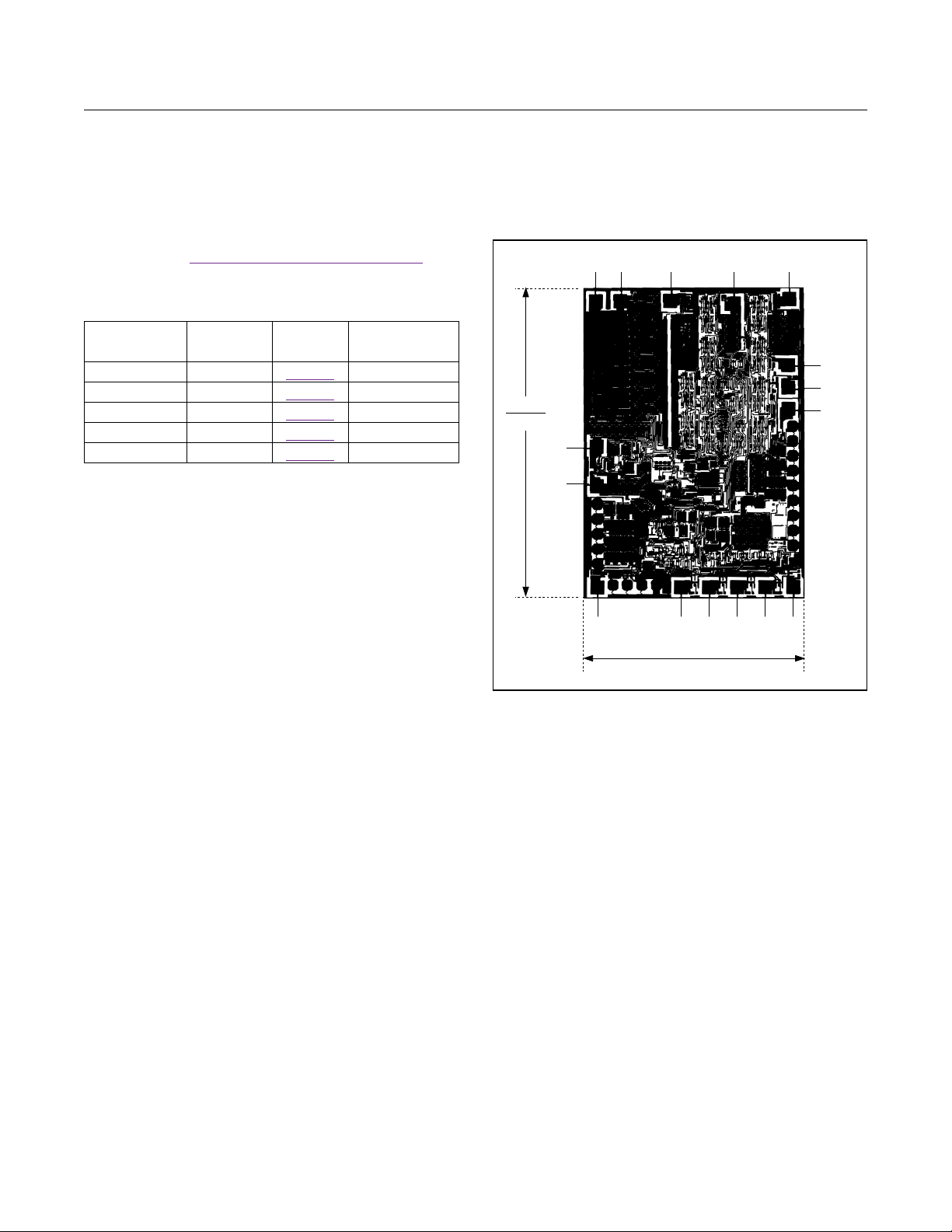
Chip Topography
V
V
CC
OUT
2
3
0.122”
(3.098 mm)
4
GND
5
BATT
ON
6
LOW LINE
V
BATT
1
OSCINOSC
(2.184 mm)
7 8
SEL
0.086”
RESET
PFI
RESET
16
9
PFO
10 11
WDI
15
14
WDO
13
CE IN
12
CE OUT
www.maximintegrated.com
Maxim Integrated
│
17
Page 18

MAX690–MAX695 Microprocessor Supervisory Circuits
Revision History
REVISION
NUMBER
5 4/15 Revised Benets and Features section 1
REVISION
DATE
DESCRIPTION
PAGES
CHANGED
For pricing, delivery, and ordering information, please contact Maxim Direct at 1-888-629-4642, or visit Maxim Integrated’s website at www.maximintegrated.com.
Maxim Integrated cannot assume responsibility for use of any circuitry other than circuitry entirely embodied in a Maxim Integrated product. No circuit patent licenses
are implied. Maxim Integrated reserves the right to change the circuitry and specications without notice at any time. The parametric values (min and max limits)
shown in the Electrical Characteristics table are guaranteed. Other parametric values quoted in this data sheet are provided for guidance.
Maxim Integrated and the Maxim Integrated logo are trademarks of Maxim Integrated Products, Inc.
©
2015 Maxim Integrated Products, Inc.
│
18
Page 19

Mouser Electronics
Authorized Distributor
Click to View Pricing, Inventory, Delivery & Lifecycle Information:
Maxim Integrated:
MAX690CPA+ MAX690EPA+ MAX691CWE+ MAX691EWE+ MAX692CPA+ MAX693CPE+ MAX693CWE+
MAX694CPA+ MAX694EPA+ MAX695CPE+ MAX695CWE+ MAX690MJA/883B MAX691MJE/883B
MAX692MJA/883B MAX693MJE/883B MAX694MJA/883B MAX695MJE/883B MAX691CPE+ MAX691CWE+T
MAX691EPE+ MAX691EWE+T MAX692EPA+ MAX693CWE+T MAX693EPE+ MAX693EWE+ MAX693EWE+T
MAX695CWE+T MAX695EPE+ MAX695EWE+ MAX695EWE+T MAX690MLP/883B MAX691MLP/883B
MAX693EJE MAX690MJA MAX691EJE MAX691EWE MAX693MJE MAX194ACWE+T MAX194ACWE+
MAX690EJA MAX691MJE
 Loading...