

Page 1
For free samples & the latest literature: http://www.maxim-ic.com, or phone 1-800-998-8800.
For small orders, phone 408-737-7600 ext. 3468.
General Description
The MAX682/MAX683/MAX684 charge-pump regulators generate 5V from a 2.7V to 5.5V input. They are
specifically designed to serve as high-efficiency auxiliary supplies in applications that demand a compact
design. The MAX682, MAX683, and MAX684 deliver
250mA, 100mA, and 50mA output current, respectively.
These complete 5V regulators require only one resistor
and three external capacitors—no inductors are needed. High switching frequencies (externally adjustable
up to 2MHz) and a unique regulation scheme allow the
use of capacitors as small as 1µF per 100mA of output
current. The MAX683/MAX684 are offered in a spacesaving 8-pin µMAX package that is only 1.1mm high,
while the MAX682 is available in an 8-pin SO.
Applications
Flash Memory Supplies
Battery-Powered Applications
Miniature Equipment
PCMCIA Cards
3.3V to 5V Local Conversion Applications
Backup-Battery Boost Converters
3V to 5V GSM SIMM Cards
Features
♦ Ultra-Small: 1µF Capacitors per 100mA of Output
Current
♦ No Inductors Required
♦ 1.1mm Height in µMAX Package (MAX683/MAX684)
♦ Up to 250mA Output Current (MAX682)
♦ Regulated ±4% Output Voltage
♦ 50kHz to 2MHz Adjustable Switching Frequency
♦ 2.7V to 5.5V Input Voltage
♦ 100µA Quiescent Current in Pulse-Skipping Mode
♦ 0.1µA Shutdown Current
MAX682/MAX683/MAX684
3.3V-Input to Regulated 5V-Output
Charge Pumps
________________________________________________________________
Maxim Integrated Products
1
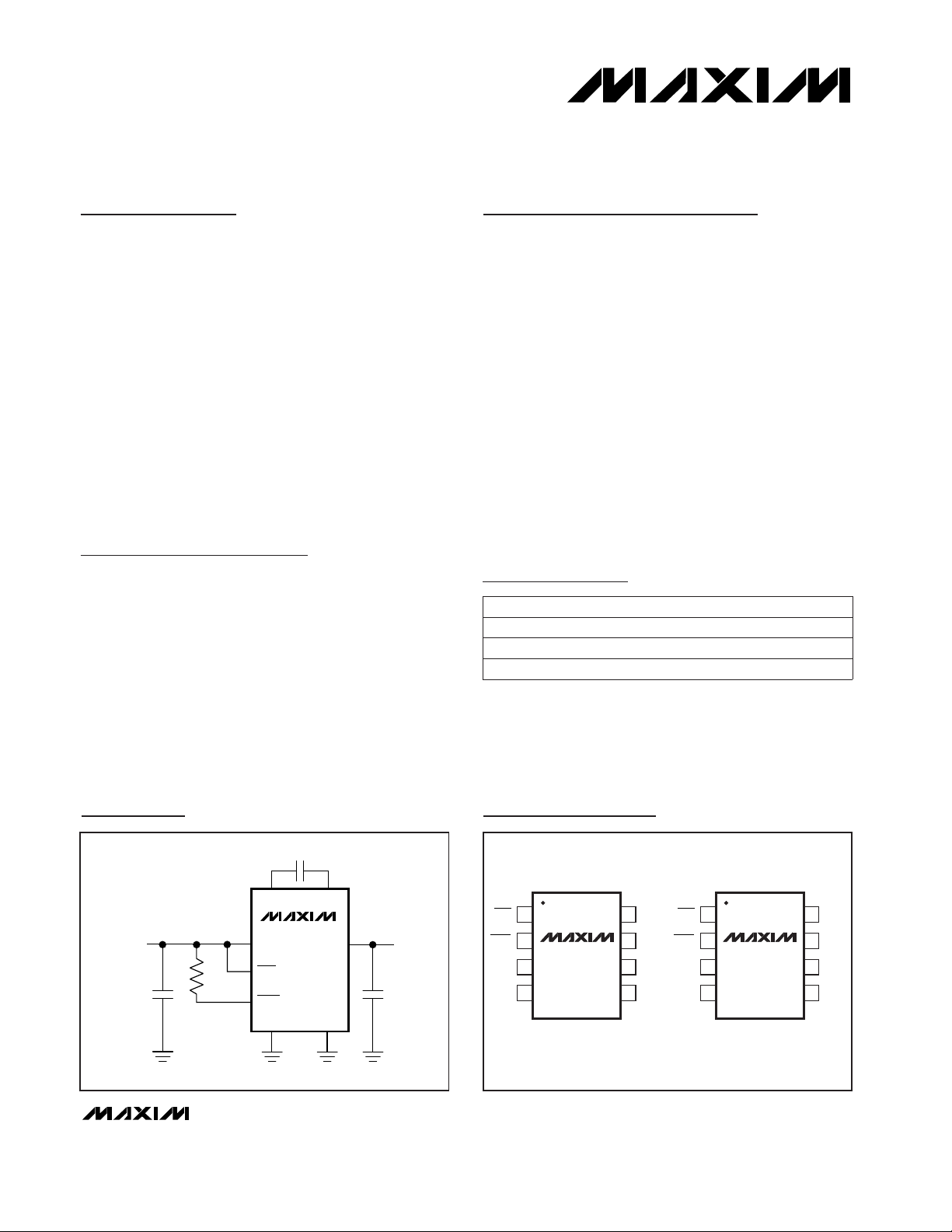
CXN
PGNDGND
1
2
87OUT
CXPSHDN
IN
SKIP
SO
TOP VIEW
3
4
6
5
MAX682
CXN
PGNDGND
1
2
87OUT
CXPSHDN
IN
SKIP
µMAX
3
4
6
5
MAX683
MAX684
Pin Configurations
OUTPUT
5V/250mA
OUT
SHDN
IN
INPUT
2.7V TO 5.5V
SKIP
R
EXT
GND PGND
CXN CXP
MAX682
Typical Operating Circuit
19-0177; Rev 1; 8/98
PART
MAX682ESA
MAX683EUA
MAX684EUA -40°C to +85°C
-40°C to +85°C
-40°C to +85°C
TEMP. RANGE PIN-PACKAGE
8 SO
8 µMAX
8 µMAX
Ordering Information
Page 2
3.0V ≤ IN ≤ 3.6V for SKIP = 0,
MAX682/MAX683/MAX684
3.3V-Input to Regulated 5V-Output
Charge Pumps
2 _______________________________________________________________________________________
ABSOLUTE MAXIMUM RATINGS
ELECTRICAL CHARACTERISTICS
(VIN= 3V, V
SKIP
= 0V, CIN= 1µF, CX= 0.47µF, C
OUT
= 2µF, I
SHDN
= 22µA; I
MAX
= 250mA for MAX682, I
MAX
= 100mA for MAX683,
I
MAX
= 50mA for MAX684; TA= T
MIN
to T
MAX
, unless otherwise noted. Typical values are at TA= +25°C.) (Note 1)
Stresses beyond those listed under “Absolute Maximum Ratings” may cause permanent damage to the device. These are stress ratings only, and functional
operation of the device at these or any other conditions beyond those indicated in the operational sections of the specifications is not implied. Exposure to
absolute maximum rating conditions for extended periods may affect device reliability.
IN, OUT, SHDN, SKIP to GND.................................-0.3V to +6V
PGND to GND.....................................................................±0.3V
CXN to GND ................................................-0.3V to (V
IN
+ 0.3V)
CXP to GND..............................................-0.3V to (V
OUT
+ 0.3V)
Continuous Output Current
MAX682........................................................................300mA
MAX683........................................................................150mA
MAX684..........................................................................75mA
Output Short-Circuit Duration...............................................5sec
Continuous Power Dissipation (T
A
= +70°C)
8-Pin SO (derate 5.9mW/°C above +70°C).................471mW
8-Pin µMAX (derate 4.1mW/°C above +70°C)............330mW
Operating Temperature Range
MAX68_E_A....................................................-40°C to +85°C
Junction Temperature......................................................+150°C
Storage Temperature Range.............................-65°C to +160°C
Lead Temperature (soldering, 10sec).............................+300°C
Regulation with VIN> 3.6V requires
SKIP = high
RL= 5V/I
MAX
(Note 2)
TA= +25°C
I
SHDN
=4.4µA
MAX682
SKIP = 0, VIN= 3.6V
SKIP = high, 0 ≤ I
LOAD
≤ I
MAX
I
SHDN
= 22µA
CONDITIONS
µs50t
START
Shutdown Exit Time
160 200 250
750 1000 1300
kHz
850 1000 1200
Switching Frequency (Note 2)
mV100
Input Undervoltage Lockout
Hysteresis
V2.0 2.35 2.6
V2.7 5.5V
IN
Input Voltage Range
Input Undervoltage Lockout
Threshold
µA1 50I
SHDN
SHDN Input Current Range
mV630 690 750V
ON, SHDN
SHDN On Bias Voltage
V0.35V
INL, SHDN
SHDN Logic Low Input
mA
250
I
MAX
Maximum Output Current
mA
0.1 0.18
I
Q
No-Load Input Current
%-3∆V
LDR
Load Regulation
UNITSMIN TYP MAXSYMBOLPARAMETER
0°C < TA< +85°C
-40°C < TA< +85°C
0°C < TA< +85°C
150 200 270-40°C < TA< +85°C
MAX683 100
MAX684 50
7.5
SHDN = 0, VIN= 5.5V, V
OUT
= 0
µA0.1 5I
Q, SHDN
Shutdown Supply Current
0 < I
LOAD
≤ I
MAX
;
3.0V ≤ IN ≤ 3.6V for SKIP = 0,
3.0V ≤ IN ≤ 5.5V for SKIP = IN
V4.80 5.05 5.20V
OUT
Output Voltage
2.5
SKIP = VIN= 3.6V
1.7MAX684
MAX683
MAX682
Page 3
MAX682/MAX683/MAX684
3.3V-Input to Regulated 5V-Output
Charge Pumps
_______________________________________________________________________________________ 3
ELECTRICAL CHARACTERISTICS (continued)
(VIN= 3V, V
SKIP
= 0V, CIN= 1µF, CX= 0.47µF, C
OUT
= 2µF, I
SHDN
= 22µA; I
MAX
= 250mA for MAX682, I
MAX
= 100mA for MAX683,
I
MAX
= 50mA for MAX684; TA= T
MIN
to T
MAX
, unless otherwise noted. Typical values are at TA= +25°C.) (Note 1)
Note 1: Specifications to -40°C are guaranteed by design and not production tested.
Note 2: Current into SHDN determines oscillator frequency: R
EXT
(kΩ) = 45000 (VIN- 0.69V) / f
OSC
(kHz)
VIN= 5.5V, V
SKIP
= 0V or 5.5V
VIN= 5.5V
CONDITIONS
µA-1 1I
SKIP
SKIP Input Leakage Current
2.4V
INH, SKIP
SKIP Input Voltage High
V
0.8V
INL, SKIP
SKIP Input Voltage Low
UNITSMIN TYP MAXSYMBOLPARAMETER
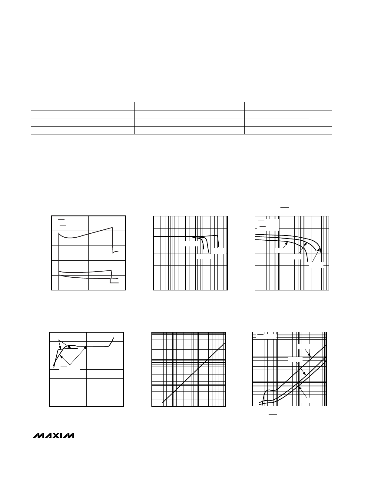
__________________________________________Typical Operating Characteristics
(Circuit of Figure 5, VIN= 3.3V, component values from Tables 2 and 3, TA = +25°C, unless otherwise noted.)
0
2
6
MAX682
MAX683
MAX684
4
8
10
2 3 4 5 6
NO-LOAD SUPPLY CURRENT
vs. SUPPLY VOLTAGE
MAX682 TOC01
SUPPLY VOLTAGE (V)
SUPPLY CURRENT (mA)
SKIP = HIGH
I
SHDN
= 22µA
5.50
4.00
1 10 100 1000
OUTPUT VOLTAGE vs. LOAD CURRENT
(SKIP = LOW)
MAX682 TOC03
LOAD CURRENT (mA)
OUTPUT VOLTAGE (V)
4.50
5.00
5.25
4.25
4.75
MAX684
MAX683
MAX682
5.50
4.00
1 10 100 1000
OUTPUT VOLTAGE vs. LOAD CURRENT
(SKIP = HIGH)
MAX682 TOC04
LOAD CURRENT (mA)
OUTPUT VOLTAGE (V)
4.50
5.00
5.25
4.25
4.75
MAX684
MAX683
MAX682
SKIP = HIGH
I
SHDN
= 22µA
3.50
3.75
4.00
4.25
4.50
4.75
5.00
5.25
5.50
2 3 4 5 6
OUTPUT VOLTAGE
vs. SUPPLY VOLTAGE
MAX682 TOC06
SUPPLY VOLTAGE (V)
OUTPUT VOLTAGE (V)
SKIP = HIGH
SKIP = LOW
10M
10k
0.1 1 10 100
OSCILLATOR FREQUENCY vs.
SHUTDOWN PIN INPUT CURRENT
MAX682 TOC08
SHDN INPUT CURRENT (µA)
OSCILLATOR FREQUENCY (Hz)
100k
1M
100
0.1
0.1 1 10 100
NO-LOAD SUPPLY CURRENT vs.
SHUTDOWN PIN INPUT CURRENT
MAX682 TOC09
SHDN INPUT CURRENT (µA)
NO-LOAD SUPPLY CURRENT (mA)
1
10
MAX683
MAX682
MAX684
SKIP = HIGH
Page 4
MAX682/MAX683/MAX684
3.3V-Input to Regulated 5V-Output
Charge Pumps
4 _______________________________________________________________________________________
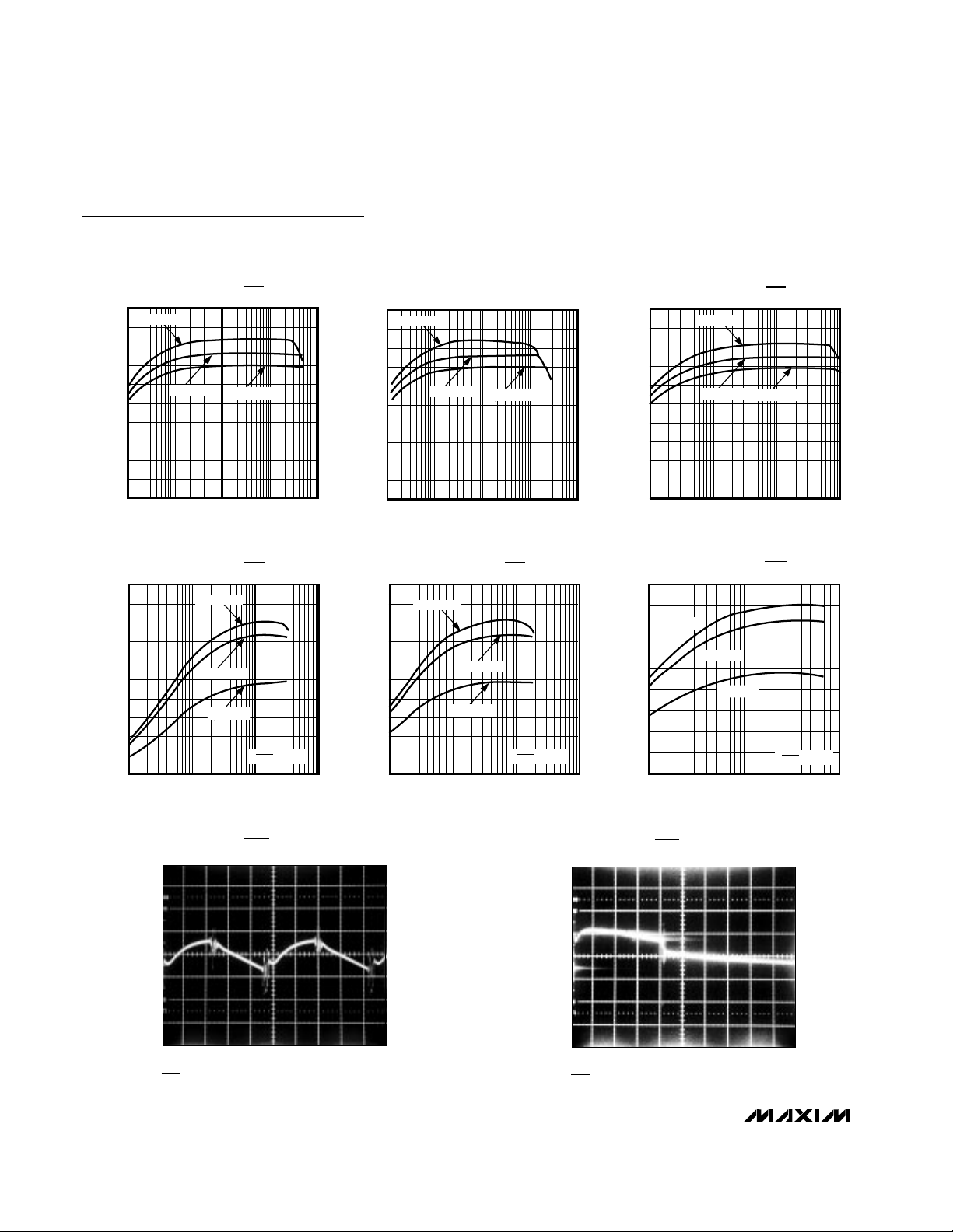
Typical Operating Characteristics (continued)
(Circuit of Figure 5, VIN= 3.3V, component values from Tables 2 and 3, TA = +25°C, unless otherwise noted.)
100
0
1 10 100 1000
MAX682 EFFICIENCY
vs. LOAD CURRENT (SKIP = HIGH)
20
10
MAX682 TOC13
LOAD CURRENT (mA)
EFFICIENCY (%)
50
70
60
40
30
80
90
VIN = 5.0V
VIN = 3.3V
VIN = 3.0V
I
SHDN
= 22µA
100
0
1 10 100 1000
MAX683 EFFICIENCY
vs. LOAD CURRENT (SKIP = HIGH)
20
10
MAX682 TOC14
LOAD CURRENT (mA)
EFFICIENCY (%)
50
70
60
40
30
80
90
VIN = 5.0V
VIN = 3.3V
VIN = 3.0V
I
SHDN
= 22µA
90
0
1 10 100
MAX684 EFFICIENCY
vs. LOAD CURRENT (SKIP = HIGH)
20
10
MAX682 TOC15
LOAD CURRENT (mA)
EFFICIENCY (%)
40
30
50
60
70
80
VIN = 3.0V
VIN = 3.3V
VIN = 5.0V
I
SHDN
= 22µA
200ns/div
OUTPUT WAVEFORM
(SKIP = HIGH)
MAX682 TOC16
50mV/div
SKIP = HIGH, I
SHDN
= 22µA, I
LOAD
= 250mA, MAX682
200ns/div
OUTPUT WAVEFORM
(SKIP = LOW)
MAX682 TOC17
50mV/div
SKIP = LOW, I
LOAD
= 250mA, MAX682
100
0
0.1 1 10 100 1000
MAX682 EFFICIENCY
vs. LOAD CURRENT (SKIP = LOW)
20
10
MAX682 TOC10
LOAD CURRENT (mA)
EFFICIENCY (%)
50
70
60
40
30
80
90
VIN = 3.6V
VIN = 3.3V
VIN = 3.0V
100
0
0.1 1 10 100 1000
MAX683 EFFICIENCY
vs. LOAD CURRENT (SKIP = LOW)
20
10
MAX682 TOC11
LOAD CURRENT (mA)
EFFICIENCY (%)
50
70
60
40
30
80
90
VIN = 3.6V
VIN = 3.3V
VIN = 3.0V
100
0
0.1 1 10 100
MAX684 EFFICIENCY
vs. LOAD CURRENT (SKIP = LOW)
20
10
MAX682 TOC12
LOAD CURRENT (mA)
EFFICIENCY (%)
50
70
60
40
30
80
90
VIN = 3.6V
VIN = 3.3V
VIN = 3.0V
Page 5

MAX682/MAX683/MAX684
3.3V-Input to Regulated 5V-Output
Charge Pumps
_______________________________________________________________________________________ 5
2ms/div
LOAD-TRANSIENT RESPONSE
MAX682 TOC19
A
B
A: LOAD CURRENT: I
LOAD
= 5mA TO 250mA, 500mA/div
B: OUTPUT VOLTAGE: SKIP = HIGH, I
SHDN
= 22µA,
100mV/div, MAX682
100µs/div
SHUTDOWN TIMING
MAX682 TOC18
A
B
A: OUTPUT VOLTAGE: SKIP = HIGH, R
L
= 5V / I
MAX
, 2V/div
B: SHDN VOLTAGE: 1V/div
2ms/div
LINE-TRANSIENT RESPONSE
MAX682 TOC20
A
B
A: INPUT VOLTAGE: V
IN
= 3.1V TO 3.6V, 500mV/div
B: OUTPUT VOLTAGE: SKIP = HIGH, I
SHDN
= 22µA,
I
LOAD
= 250mA, 50mV/div, MAX682
Typical Operating Characteristics (continued)
(Circuit of Figure 5, VIN= 3.3V, component values from Tables 2 and 3, TA = +25°C, unless otherwise noted.)
Pin Description
NAME FUNCTION
1
SKIP
When SKIP = low, the regulator operates in low-quiescent-current skip mode. When SKIP = high, the
regulator operates in constant-frequency mode, minimizing output ripple and noise. SKIP must be tied
high for input voltages above 3.6V.
2
SHDN
Shutdown Input. Drive SHDN through an external resistor. When SHDN = low, the device turns off. When
current is sourced into SHDN through R
EXT
, the device activates, and the SHDN pin input current sets the
oscillator’s switching frequency. R
EXT
(kΩ) = 45000 (V
IN
- 0.69V) / f
OSC
(kHz).
PIN
3 IN
Input Supply Pin. Can range from 2.7V to 5.5V for SKIP = high, and 2.7V to 3.6V for SKIP = low. Bypass to
PGND with a suitable value capacitor (see
Capacitor Selection
section).
4 GND Ground Pin. Connect to PGND through a short trace.
8 OUT Fixed 5V Power Output. Bypass to PGND with output filter capacitor.
7 CXP Positive Terminal of the Charge-Pump Transfer Capacitor
6 CXN Negative Terminal of the Charge-Pump Transfer Capacitor
5 PGND Power Ground Pin
Page 6

MAX682/MAX683/MAX684
3.3V-Input to Regulated 5V-Output
Charge Pumps
6 _______________________________________________________________________________________
Detailed Description
The MAX682/MAX683/MAX684 charge pumps provide
a regulated 5V output from a 2.7V to 5.5V input. They
deliver a maximum of 250mA, 100mA, or 50mA load
current, respectively. Designed specifically for compact applications, a complete regulator circuit requires
only three small external capacitors and one resistor.
An externally adjustable switching frequency and innovative control scheme allow the circuit to be optimized
for efficiency, size, or output noise. The devices also
contain a shutdown feature.
The MAX682/MAX683/MAX684 consist of an error
amplifier, a 1.23V bandgap reference, an internal resistive feedback network, an oscillator, high-current MOSFET switches, and shutdown and control logic (Figure
1). Figure 2 shows an idealized unregulated chargepump voltage doubler. The oscillator runs at a 50%
duty cycle. During one half of the period, the transfer
capacitor (CX) charges to the input voltage. During the
other half, the doubler stacks the voltage across C
X
and the input voltage, and transfers the sum of the two
voltages to the output filter capacitor (C
OUT
). Rather
than simply doubling the input voltage, the
MAX682/MAX683/MAX684 provide a regulated fixed
output voltage (5V) using either skip mode or constantfrequency mode. Skip mode and constant-frequency
mode are externally selected via the SKIP input pin.
Skip Mode
In skip mode (SKIP = low), the error amplifier disables
switching when it detects an output higher than 5V. The
device then skips switching cycles until the output voltage drops. Then the error amplifier reactivates the
oscillator. Figure 3 illustrates the regulation scheme.
This regulation method minimizes operating current
because the device does not switch continuously. SKIP
is a logic input and should not remain floating.
Constant-Frequency Mode
When SKIP is high, the charge pump runs continuously
at the selected frequency. Figure 4 shows a block diagram of the device in constant-frequency mode. The
error amplifier controls the charge on CXby driving the
gate of the N-channel FET. When the output voltage
falls, the gate drive increases, resulting in a larger voltage across CX. This regulation scheme minimizes output ripple. Since the device switches continuously, the
CXP
OUT
1.23V
EN
SHDN
PGND
SWITCHES
CONTROL
LOGIC
CXN
SHDN
SKIP
IN
OSC
Figure 2. Unregulated Voltage Doubler
IN
S1
S2
C
IN
C
X
OUT
OSCILLATOR
EN
Figure 3. Skip-Mode Regulation
Figure 1. Functional Block Diagram
IN
C
S1
C
IN
X
OSC
S2
OUT
C
OUT
Page 7

MAX682/MAX683/MAX684
3.3V-Input to Regulated 5V-Output
Charge Pumps
_______________________________________________________________________________________ 7
output noise contains well-defined frequency components, and the circuit requires much smaller external
capacitors for a given output ripple. However, constantfrequency mode, due to higher operating current, is
less efficient at light loads than skip mode. Note: For
input voltages above 3.6V, the devices must operate in
constant-frequency mode. Table 1 summarizes the
tradeoffs between the two operating modes.
Frequency Selection and Shutdown
The SHDN pin on the MAX682/MAX683/MAX684 performs a dual function: it shuts down the device and
determines the oscillator frequency. The SHDN input
looks like a diode to ground and should be driven
through a resistor.
Driving SHDN low places the device in shutdown
mode. This disables all switches, the oscillator, and
control logic. The device typically draws 0.1µA (5µA
max) of supply current in this mode and the output presents a 50kΩ impedance to ground. The device exits
shutdown once SHDN is forward biased (minimum of
1µA of current). The typical no-load shutdown exit time
is 50µs.
When SHDN is pulled high through an external resistor
to V
IN
, the bias current into SHDN determines the
charge-pump frequency. To select the frequency, calculate the external resistor value, R
EXT
, using the fol-
lowing formula:
R
EXT
= 45000 (V
IN
- 0.69V) / f
OSC
where R
EXT
is in kΩ and f
OSC
is in kHz. Program the
frequency in the 50kHz to 2MHz range. This frequency
range corresponds to SHDN input currents between
1µA and 50µA. Proper operation of the oscillator is not
guaranteed beyond these limits. Currents lower than
1µA may shut down the device. The forward-biased
diode voltage from the SHDN input to GND has a temperature coefficient of -2mV/°C.
Undervoltage Lockout
The MAX682/MAX683/MAX684 have an undervoltagelockout feature that deactivates the devices when the
input voltage falls below 2.25V. Regulation at low input
voltages cannot be maintained. This safety feature
ensures that the device shuts down before the output
voltage falls out of regulation by a considerable amount
(typically 10% with no load). Once deactivated, hysteresis holds the device in shutdown until the input voltage rises 100mV above the lockout threshold.
Applications Information
Capacitor Selection
The MAX682/MAX683/MAX684 require only three external capacitors (Figure 5). Their values are closely linked
to the output current capacity, oscillator frequency, output noise content, and mode of operation.
Generally, the transfer capacitor (CX) will be the smallest, and the input capacitor (CIN) is twice as large as
CX. Higher switching frequencies allow the use of
smaller CXand CIN. The output capacitor (C
OUT
) can
be anywhere from 5-times to 50-times larger than CX,
depending on the mode of operation and ripple tolerance. In continuous switching mode, smaller output ripple allows smaller C
OUT
. In skip mode, a larger C
OUT
is
required to maintain low output ripple. Tables 2 and 3
show capacitor values recommended for lowest supply-current operation (skip mode) and smallest size operation (constant-frequency mode), respectively.
IN
S1
S2
C
IN
C
OUT
C
X
OUT
OSC
N-CHANNEL
Figure 4. Constant-Frequency-Mode Regulation
FEATURE
SKIP MODE
(
SKIP = LOW)
CONSTANT-
FREQUENCY MODE
(SKIP = HIGH)
Best Light-Load
Efficiency
✔
Smallest External
Component Size
✔
Output Ripple
Amplitude and
Frequency
Relatively large
amplitude, variable
frequency
Relatively small
amplitude, constant
frequency
Load Regulation Very Good Good
Table 1. Tradeoffs Between Operating
Modes
Page 8

MAX682/MAX683/MAX684
In addition, the following two equations approximate
output ripple for each mode. In skip mode, output ripple is dominated by ESR, and is approximately:
V
RIPPLE(SKIP)
≅ (2V
IN
- V
OUT
)ESR
COUT
/ R
TX
where ESR
COUT
is the ESR of the output filter capacitance, and RTXis the open-loop output transfer resistance of the IC. RTXis typically 0.8Ω for the MAX682,
1.6Ω for the MAX683, and 3Ω for the MAX684. In constant-frequency mode, output ripple is dominated by
C
OUT
and is approximately:
V
RIPPLE(const-freq)
≅ I
OUT
/ (2 x f
OSC
x C
OUT
)
All capacitors must maintain a low (<100mΩ) equivalent series resistance (ESR). Table 4 lists the manufacturers of recommended capacitors. Surface-mount
tantalum capacitors will work well for most applications.
Ceramic capacitors will provide the lowest ripple due to
their typically lower ESR.
If the source impedance or inductance of the input supply is large, additional input bypassing (2.2µF to 22µF)
may be needed. This additional capacitance need not
be a low-ESR type.
3.3V-Input to Regulated 5V-Output
Charge Pumps
8 _______________________________________________________________________________________
PART
C
IN
(µF)
MAX682 2.2 47
MAX683 1 22
MAX684 0.47 10
V
OUT
RIPPLE
(mV)
100
100
100
C
X
(µF)
1
0.47
0.22
OUTPUT
(mA)
250
100
50
Table 2. Recommended Capacitor Values
for Quiescent Current (Skip Mode)
Table 3. Recommended Capacitor Values
for Smallest Size (Constant-Frequency
Mode, I
SSHHDDNN
= 22µA, 1MHz)
PART
C
IN
(µF)
CERAMIC
C
OUT
(µF)
MAX682 1 2.2
MAX683 0.47 1
MAX684 0.22 0.47
V
OUT
RIPPLE
(mV)
80
80
80
C
X
(µF)
0.47
0.22
0.1
OUTPUT
(mA)
250
100
50
MANUFACTURER
PHONE
NUMBER
Sprague (603) 224-1961
AVX (803) 946-0690
VALUE
47µF to
10µF
47µF to
10µF
Figure 6. Paralleling Two MAX682s
TDK (847) 390-4373
0.1µF to
2.2µF
Table 4. Recommended Capacitor
Manufacturers
C
X
C
IN
C
OUT
OUT
CXN
CXP
SHDN
IN
OUT
7
4 5
6
3
2
1
8
ON
OFF
R
EXT
SKIP
GND PGND
MAX682
MAX683
MAX684
IN
V
ON
Figure 5. Standard Operating Circuit
TANTALUM
C
OUT
(µF)
10
4.7
2.2
CERAMIC
Ceramic
surface mount
DESCRIPTION
595D-series
tantalum
surface mount
TPS-series
surface mount
3.3V
IN
SKIP
100k 100k
1µF
0.47µF
SHDN
CXP
CXN
OUTIN
MAX682
GND PGND
1µF
0.47µF
IN
SKIP
MAX682
SHDN
CXP
CXN
GND PGND
OUT
5V/500mA
4.7µF
Page 9

MAX682/MAX683/MAX684
3.3V-Input to Regulated 5V-Output
Charge Pumps
_______________________________________________________________________________________ 9
Power Dissipation
The power dissipated in the MAX682/MAX683/MAX684
depends on output current and is accurately described
by:
P
DISS
= I
OUT
(2VIN- V
OUT
)
P
DISS
must be less than that allowed by the package
rating. See the
Absolute Maximum Ratings
for 8-pin
µMAX (MAX683/MAX684) and SO (MAX682) powerdissipation limits and deratings.
Layout Considerations
All capacitors should be soldered in close proximity to
the IC. Connect ground and power ground through a
short, low-impedance trace. If a high-value resistor is
driving the shutdown input and is picking up noise (i.e.,
frequency jitter at CXP and CXN), bypass SHDN to
GND with a small capacitor (0.01µF).
Paralleling Devices
The MAX682/MAX683/MAX684 can be paralleled to
yield higher load currents. The circuit of Figure 6 can
deliver 500mA at 5V. It uses two MAX682s in parallel.
The devices can share the output capacitors, but each
one requires its own transfer capacitor (CX) and input
capacitor. For best performance, the paralleled devices
should operate in the same mode (skip or constant frequency).
Chip Information
TRANSISTOR COUNT: 659
SUBSTRATE CONNECTED TO GND
Package Information
8LUMAXD.EPS
Page 10

MAX682/MAX683/MAX684
3.3V-Input to Regulated 5V-Output
Charge Pumps
10 ______________________________________________________________________________________
Package Information
SOICN.EPS
Page 11

MAX682/MAX683/MAX684
3.3V-Input to Regulated 5V-Output
Charge Pumps
______________________________________________________________________________________ 11
NOTES
Page 12

MAX682/MAX683/MAX684
3.3V-Input to Regulated 5V-Output
Charge Pumps
Maxim cannot assume responsibility for use of any circuitry other than circuitry entirely embodied in a Maxim product. No circuit patent licenses are
implied. Maxim reserves the right to change the circuitry and specifications without notice at any time.
12
____________________Maxim Integrated Products, 120 San Gabriel Drive, Sunnyvale, CA 94086 408-737-7600
© 1998 Maxim Integrated Products Printed USA is a registered trademark of Maxim Integrated Products.
NOTES
 Loading...