

Page 1
General Description
The MAX6826–MAX6831 are ultra-low-voltage microprocessor (µP) supervisory circuits designed to monitor
two power supplies and have manual reset and watchdog input functions. These devices assert a system reset
if any of the monitored supplies fall below the preprogrammed thresholds, and maintain reset for a minimum
timeout period after the supplies rise above the threshold.
Microprocessor supervisors significantly improve system
reliability and accuracy compared to separate ICs or discrete components. These devices monitor primary voltages from +1.8V to +5.0V and secondary voltages from
+0.9V to +2.5V. These devices are guaranteed to be in
the correct state for VCCdown to +1.0V.
A variety of preprogrammed reset threshold voltages
are available (see Threshold Suffix Guide). The devices
include manual reset and watchdog inputs. The
MAX6829/MAX6830/MAX6831 provide a factorytrimmed threshold to monitor a 2nd voltage down to
+0.9V. The MAX6826/MAX6829 have a push-pull
RESET, the MAX6827/MAX6830 have a push-pull
RESET and the MAX6828/MAX6831 have an open-drain
RESET. The MAX6826/MAX6827/MAX6828 have an auxiliary monitor that allows user adjustable input to monitor
voltages down to +0.6V. See Selector Guide for functions available.
________________________Applications
Features
♦ Monitor Primary VCCSupplies from +1.8V
to +5.0V and Secondary V
CC2
Supplies
from +0.9V to +2.5V
♦ User Adjustable RESET IN Down to +0.63V
(MAX6826/MAX6827/MAX6828)
♦ 140ms (min) Reset Timeout Delay
♦ 1.6s Watchdog Timeout Period
♦ Manual Reset Input
♦ Three Reset Output Options
Push-Pull RESET
Push-Pull RESET
Open-Drain RESET
♦ Guaranteed Reset Valid Down to V
CC
= +1.0V
♦ Immune to Short Negative V
CC
Transients
♦ No External Components
♦ Small 6-pin SOT23 Packages
MAX6826–MAX6831
Dual Ultra-Low-Voltage SOT23 µP Supervisors
with Manual Reset and Watchdog Timer
________________________________________________________________ Maxim Integrated Products 1
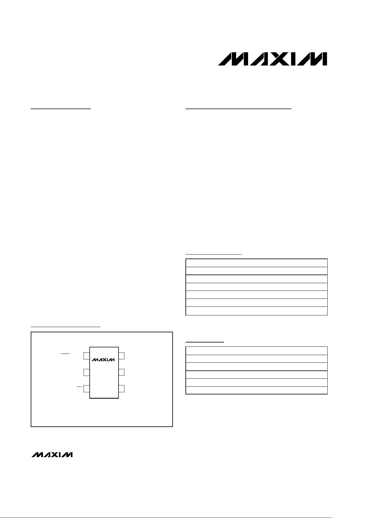
GND
WDIMR
16V
CC
5 RESET IN/V
CC2
RESET(RESET)
(RESET) MAX6827/MAX6830 ONLY
RESET IN FOR MAX6826/MAX6827/MAX6828 ONLY
V
CC2
FOR MAX6829/MAX6830/MAX6831 ONLY
MAX6826–
MAX6831
SOT23-6
TOP VIEW
2
34
Pin Configuration
19-1867; Rev 1; 1/02
Ordering Information
Standard Versions Table*
†
Insert the desired suffix letter (from Standard Versions table) into
the blanks to complete the part number.
PART
†
TEMP RANGE PIN-PACKAGE
MAX6826_UT-T -40°C to +125°C 6 SOT23-6
MAX6827_UT-T -40°C to +125°C 6 SOT23-6
MAX6828_UT-T -40°C to +125°C 6 SOT23-6
MAX6829_ _UT-T -40°C to +125°C 6 SOT23-6
MAX6830_ _UT-T -40°C to +125°C 6 SOT23-6
M AX6831_ _UT-T -40°C to +125°C 6 SOT23-6
MAX6826/MAX6827/MAX6828
L
S
R
Z
V
*Samples are typically available for standard versions only.
The MAX6826/MAX6827/MAX6828 require a 2.5k minimum
order increment for all versions. Contact factory for availability.
Portable/BatteryPowered Equipment
Embedded Controllers
Intelligent Instruments
Automotive Systems
Critical µP Monitoring
Multivoltage Systems
Typical Operating Circuit appears at end of data sheet.
Threshold Suffix Guide appears at end of data sheet.
Selector Guide appears at end of data sheet.
Standard Versions Table continued at end of data sheet.
For pricing, delivery, and ordering information, please contact Maxim/Dallas Direct! at
1-888-629-4642, or visit Maxim’s website at www.maxim-ic.com.
Page 2
MAX6826–MAX6831
Dual Ultra-Low-Voltage SOT23 µP Supervisors
with Manual Reset and Watchdog Timer
2 _______________________________________________________________________________________
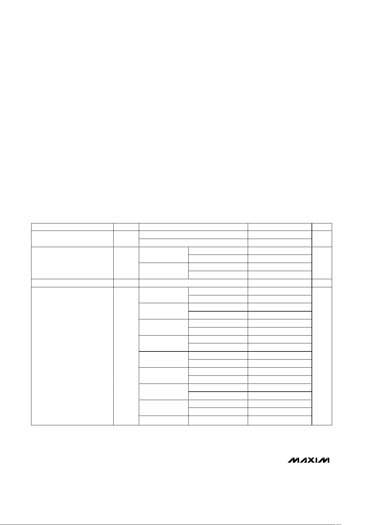
ABSOLUTE MAXIMUM RATINGS
ELECTRICAL CHARACTERISTICS
(VCC= +4.5V to +5.5V for MAX68_ _L/M, VCC= +2.7V to +3.6V for MAX68_ _T/S/R, VCC= +2.1V to +2.75V for MAX68_ _Z/Y,
V
CC
= +1.53V to +2.0V for MAX68_ _W/V; TA= -40°C to +125°C, unless otherwise specified. Typical values are at TA = +25°C.) (Note 1)
Stresses beyond those listed under “Absolute Maximum Ratings” may cause permanent damage to the device. These are stress ratings only, and functional
operation of the device at these or any other conditions beyond those indicated in the operational sections of the specifications is not implied. Exposure to
absolute maximum rating conditions for extended periods may affect device reliability.
VCC, V
CC2
to GND.................................................-0.3V to +6.0V
Open-Drain RESET................................................-0.3V to +6.0V
Push-Pull RESET, RESET............................-0.3V to (V
CC
+ 0.3V)
MR, WDI, RESET IN....................................-0.3V to (V
CC
+ 0.3V)
Input Current (V
CC
).............................................................20mA
Output Current (RESET, RESET).........................................20mA
Continuous Power Dissipation (T
A
= +70°C)
6-Pin SOT23 (derate 8.7mW/°C above +70°C)..............696mW
Operating Temperature Range .........................-40°C to +125°C
Junction Temperature......................................................+150°C
Storage Temperature Range .............................-65°C to +150°C
Lead Temperature (soldering, 10s) .................................+300°C
PARAMETER SYMBOL CONDITIONS MIN TYP MAX UNITS
TA = 0°C to +85°C 1.0 5.5
Operating Voltage Range V
CC
TA = -40°C to +125°C 1.2 5.5
V
TA = -40°C to +85°C1020
VCC = +5.5V,
no load
T
A
= -40°C to +125°C30
TA = -40°C to +85°C716
VCC Supply Current
MR and WDI Unconnected
I
CC
VCC = +3.6V,
no load
T
A
= -40°C to +125°C25
µA
V
CC2
Supply Current V
CC2
≤ +2.5V 2 µA
TA = -40°C to +85°C 4.50 4.63 4.75
MAX68_ _L
T
A
= -40°C to +125°C 4.47 4.63 4.78
TA = -40°C to +85°C 4.25 4.38 4.50
MAX68_ _M
T
A
= -40°C to +125°C 4.22 4.38 4.53
TA = -40°C to +85°C 3.00 3.08 3.15
MAX68_ _T
T
A
= -40°C to +125°C 2.97 3.08 3.17
TA = -40°C to +85°C 2.85 2.93 3.00
MAX68_ _S
T
A
= -40°C to +125°C 2.83 2.93 3.02
TA = -40°C to +85°C 2.55 2.63 2.70
MAX68_ _R
T
A
= -40°C to +125°C 2.53 2.63 2.72
TA = -40°C to +85°C 2.25 2.32 2.38
MAX68_ _Z
T
A
= -40°C to +125°C 2.24 2.32 2.40
TA = -40°C to +85°C 2.12 2.19 2.25
MAX68_ _Y
T
A
= -40°C to +125°C 2.11 2.19 2.26
TA = -40°C to +85°C 1.62 1.67 1.71
MAX68_ _W
T
A
= -40°C to +125°C 1.61 1.67 1.72
VCC Reset Threshold
(V
CC
Falling)
V
TH
MAX68_ _V TA = -40°C to +85°C 1.52 1.58 1.62
V
Page 3
MAX6826–MAX6831
Dual Ultra-Low-Voltage SOT23 µP Supervisors
with Manual Reset and Watchdog Timer
_______________________________________________________________________________________ 3
ELECTRICAL CHARACTERISTICS (continued)
(VCC= +4.5V to +5.5V for MAX68_ _L/M, VCC= +2.7V to +3.6V for MAX68_ _T/S/R, VCC= +2.1V to +2.75V for MAX68_ _Z/Y,
V
CC
= +1.53V to +2.0V for MAX68_ _W/V; TA= -40°C to +125°C, unless otherwise specified. Typical values are at TA = +25°C.) (Note 1)
PARAMETER SYMBOL CONDITIONS MIN TYP MAX UNITS
TA = -40°C to +85°C 2.244 2.313 2.381
Z
T
A
= -40°C to +125°C 2.238 2.313 2.388
TA = -40°C to +85°C 2.119 2.188 2.257
Y
T
A
= -40°C to +125°C 2.113 2.188 2.263
TA = -40°C to +85°C 1.615 1.665 1.715
W
T
A
= -40°C to +125°C 1.611 1.665 1.719
TA = -40°C to +85°C 1.525 1.575 1.625
V
T
A
= -40°C to +125°C 1.521 1.575 1.629
TA = -40°C to +85°C 1.346 1.388 1.429
I
T
A
= -40°C to +125°C 1.343 1.388 1.433
TA = -40°C to +85°C 1.271 1.313 1.354
H
T
A
= -40°C to +125°C 1.268 1.313 1.358
TA = -40°C to +85°C 1.077 1.110 1.143
G
T
A
= -40°C to +125°C 1.074 1.110 1.146
TA = -40°C to +85°C 1.017 1.050 1.083
F
T
A
= -40°C to +125°C 1.014 1.050 1.086
TA = -40°C to +85°C 0.808 0.833 0.858
E
T
A
= -40°C to +125°C 0.806 0.833 0.860
TA = -40°C to +85°C 0.762 0.788 0.813
V
CC2
Reset Threshold V
TH2
D
T
A
= -40°C to +125°C 0.761 0.788 0.815
V
Reset Threshold Temperature
Coefficient
60 ppm/°C
Reset Threshold Hysteresis 2 x V
TH
mV
TA = 0°C to +85°C 0.615 0.630 0.645
RESET IN Threshold V
RS T IN TH VRSTINTH
falling
T
A
= -40°C to +125°C 0.610 0.650
V
RESET IN Hysteresis 2.5 mV
TA = -40°C to +85°C -25 +25
RESET IN Input Current (Note 2) I
RSTIN
TA = -40°C to +125°C -100 +100
nA
VCC to Reset Output Delay t
RD
VCC = VTH to (VTH - 100mV) 20 µs
RESET IN to Reset Output Delay V
RSTIN
= V
RSTINTH
to (V
RSTINTH
- 30mV) 15 µs
TA = -40°C to +85°C 140 200 280
Reset Timeout Period t
RP
TA = -40°C to +125°C 100 320
ms
VCC ≥ 1.0V, I
SINK
= 50µA, reset asserted,
T
A
= 0°C to +85°C
0.3
VCC ≥ 1.2V, I
SINK
= 100µA, reset asserted 0.3
VCC ≥ 2.55V, I
SINK
= 1.2mA, reset asserted 0.3
RESET Output LOW
(Push-Pull or Open-Drain)
V
OL
VCC ≥ 4.25V, I
SINK
= 3.2mA, reset asserted 0.4
V
Page 4
MAX6826–MAX6831
Dual Ultra-Low-Voltage SOT23 µP Supervisors
with Manual Reset and Watchdog Timer
4 _______________________________________________________________________________________
ELECTRICAL CHARACTERISTICS (continued)
(VCC= +4.5V to +5.5V for MAX68_ _L/M, VCC= +2.7V to +3.6V for MAX68_ _T/S/R, VCC= +2.1V to +2.75V for MAX68_ _Z/Y,
V
CC
= +1.53V to +2.0V for MAX68_ _W/V; TA= -40°C to +125°C, unless otherwise specified. Typical values are at TA = +25°C.) (Note 1)
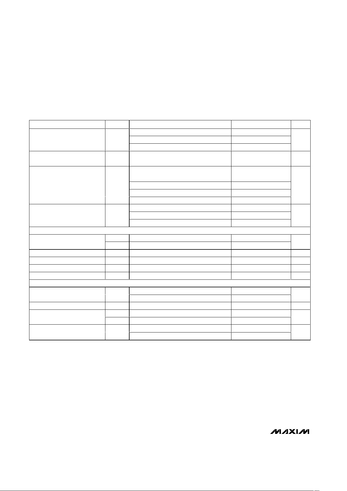
PARAMETER SYMBOL CONDITIONS MIN TYP MAX UNITS
V
C C
≥ 1.8V , I
S OURC E
= 200µA, reset not asser ted 0.8 ✕ V
C
C
V
C C
≥ 3.15V , I
S OURC E
= 500µA, reset not asser ted 0.8 ✕ V
C
C
RESET Output HIGH
(Push-Pull Only)
V
OH
V
C C
≥ 4.75V , I
S OURC E
= 800µA, reset not asser ted 0.8 ✕ V
C
C
V
Open-Drain RESET Output
Leakage Current (Note 1)
I
LKG
RESET not asserted 1.0 µA
VCC ≥ 1.0V, I
S OU RC E
= 1µA, reset asserted,
T
A
= 0°C to +85°C
0.8
✕
V
C C
V
C C
≥ 1.50V , I
S OU RC E
= 100µA, r eset asser ted 0.8 ✕ V
C C
V
C C
≥ 2.55V , I
S OU RC E
= 500µA, r eset asser ted 0.8 ✕ V
C C
RESET Output HIGH
(Push-Pull Only)
V
OH
V
C C
≥ 4.25V , I
S OU RC E
= 800µA, r eset asser ted 0.8 ✕ V
C C
V
V
C C
≥ 1.8V , I
S IN K
= 500µA, r eset asser ted 0.3
V
C C
≥ 3.15V , I
S IN K
= 1.2m A, r eset asser ted 0.3
RESET Output LOW
(Push-Pull Only)
V
OH
V
C C
≥ 4.75V , I
S IN K
= 3.2m A, r eset asser ted 0.3
V
MANUAL RESET INPUT
V
IL
0.3 ✕ V
C C
MR Input voltage
V
IH
0.7 ✕ V
C C
V
MR Minimum Input Pulse 1 µs
MR Glitch Rejection 100 ns
MR to Reset Delay 200 ns
MR Pullup Resistance 25 50 75 kΩ
WATCHDOG INPUT
TA = -40°C to +85°C 1.12 1.6 2.4
Watchdog Timeout Period t
WD
TA = -40°C to +125°C 0.80 2.60
s
WDI Pulse Width (Note 2) t
WDI
50 ns
V
IL
0.3 ✕ V
C C
WDI Input Voltage
V
IH
0.7 ✕ V
C C
V
WDI = VCC, time average 120 160
WDI Input Current I
WDI
WDI = 0, time average -20 -15
µA
Note 1: Over-temperature limits are guaranteed by design and not production tested. Devices tested at +25°C.
Note 2: Guaranteed by design and not production tested.
Page 5

MAX6826–MAX6831
Dual Ultra-Low-Voltage SOT23 µP Supervisors
with Manual Reset and Watchdog Timer
_______________________________________________________________________________________ 5
3
5
4
7
6
9
8
10
12
11
13
-40 0 20 40-20 60 80 100 120
SUPPLY CURRENT
vs. TEMPERATURE
MAX6826 toc01
TEMPERATURE (°C)
SUPPLY CURRENT (µA)
VCC = +5V, L VERSION
VCC = +3.3V, S VERSION
VCC = +1.8V, V VERSION
150
170
160
190
180
210
200
220
240
230
250
-40 0 20 40-20 60 80 100 120
RESET TIMEOUT PERIOD
vs. TEMPERATURE
MAX6826 toc02
TEMPERATURE (°C)
RESET TIMEOUT PERIOD (ms)
0
10
5
20
15
30
25
35
-40 0 20-20 40 60 80 100 120
VCC TO RESET OUTPUT DELAY
vs. TEMPERATURE
MAX6826 toc03
TEMPERATURE (°C)
PROPAGATION DELAY (µs)
VCC FALLING, VCC = VTH - 100mV
1.0
1.2
1.1
1.4
1.3
1.6
1.5
1.7
1.9
1.8
2.0
-40 0 20 40-20 60 80 100 120
WATCHDOG TIMEOUT PERIOD
vs. TEMPERATURE
MAX6826 toc04
TEMPERATURE (°C)
WATCHDOG TIMEOUT PERIOD (s)
0.94
0.96
1.00
0.98
1.04
1.02
1.06
-40 0 20-20 40 60 80 100 120
NORMALIZED RESET THRESHOLD
DELAY vs. TEMPERATURE
MAX6826 toc05
TEMPERATURE (°C)
RESET THRESHOLD (V)
0
60
40
20
80
100
120
0806020 40 100 120 140 160 180 200
MAXIMUM VCC TRANSIENT DURATION
vs. RESET THRESHOLD OVERDRIVE
MAX6826 toc06
RESET THRESHOLD OVERDRIVE (mV), VTH - V
CC
TRANSIENT DURATION (µs)
RESET OCCURS
ABOVE CURVE
0
10
5
20
15
25
-40 0 20-20 40 60 80 100 120
V
RSTIN
TO RESET OUTPUT DELAY
vs. TEMPERATURE
MAX6826 toc07
TEMPERATURE (°C)
PROPAGATION DELAY (µs)
V
RSTIN
FALLING
V
RSTIN
= V
RSTINTH
- 30mV
0
40
30
20
10
50
60
70
80
90
100
0806020 40 100 120 140 160 180 200
MAXIMUM V
RSTIN
TRANSIENT DURATION
vs. RESET THRESHOLD OVERDRIVE
MAX6826 toc08
RESET THRESHOLD OVERDRIVE (mV), V
RSTINTH
- V
RSTIN
TRANSIENT DURATION (µs)
RESET OCCURS
ABOVE CURVE
Typical Operating Characteristics
(TA = +25°C, unless otherwise noted.)
Page 6

MAX6826–MAX6831
Dual Ultra-Low-Voltage SOT23 µP Supervisors
with Manual Reset and Watchdog Timer
6 _______________________________________________________________________________________
0
0.010
0.005
0.200
0.150
0.300
0.250
0.350
0231 4567
VOLTAGE OUTPUT LOW vs. I
SINK
MAX6826 toc09
I
SINK
(mA)
V
OUT
(V)
VCC = +2.9V
Typical Operating Characteristics (continued)
(TA = +25°C, unless otherwise noted.)
2.74
2.78
2.76
2.82
2.80
2.84
2.86
2.90
2.88
2.92
0 0.1 0.2 0.3 0.4 0.5 0.6 0.7 0.8 0.9 1.0
VOLTAGE OUTPUT HIGH vs. I
SOURCE
MAX6826 toc10
I
SOURCE
(mA)
V
OUT
(V)
VCC = +2.9V
Pin Description
PIN NUMBER
MAX
6826
MAX
6827
MAX
6828
MAX
6829
MAX
6830
MAX
6831
PIN
NAME
FUNCTION
1 1 1 1 RESET
Active-Low Open-Drain or Push-Pull Reset Output. RESET changes from high
to low when V
CC1
, V
CC2
, or RESET IN input drops below the selected reset
threshold, MR is pulled low, or the watchdog triggers a reset. RESET remains
low for the reset timeout period after all voltages exceed the device reset
threshold, MR goes low to high, or the watchdog triggers a reset.
1 1 RESET
Active-High Push-Pull Reset Output. RESET changes from low to high when
V
CC1
, V
CC2
, or RESET IN input drops below the selected reset threshold, MR
is pulled low, or the watchdog triggers a reset. RESET remains HIGH for the
reset timeout period after all voltages exceed the device reset threshold, MR
goes low to high, or the watchdog triggers a reset.
2 2 2 2 2 2 GND Ground
3 3 3 3 3 3 MR
M anual Reset Inp ut, Acti ve- Low , Inter nal 50kΩ p ul l up to V
C C
. P ul l l ow to for ce a
r eset. Reset r em ai ns acti ve as l ong as M R i s l ow and for the r eset ti m eout p er i od
after M R g oes hi g h. Leave unconnected or connect to V
C C
, i f unused .
4 4 4 4 4 4 WDI
Watchd og Inp ut. If WD I r em ai ns hi g h or l ow for l ong er than the w atchd og ti m eout
p er i od , the i nter nal w atchd og ti m er r uns out and a r eset i s tr i g g er ed for the r eset
ti m eout p er i od . The i nter nal w atchd og ti m er cl ear s w henever r eset i s asser ted , the
m anual r eset i s asser ted , or WD I sees a r i si ng or fal l i ng ed g e. If WD I i s l eft
unconnected or i s connected to a thr ee- stated b uffer outp ut, the w atchd og featur e
i s d i sab l ed .
Page 7

MAX6826–MAX6831
Dual Ultra-Low-Voltage SOT23 µP Supervisors
with Manual Reset and Watchdog Timer
_______________________________________________________________________________________ 7
Pin Description (continued)
PIN NUMBER
MAX
6826
MAX
6827
MAX
6828
MAX
6829
MAX
6830
MAX
6831
PIN
NAME
FUNCTION
5 5 5
RESET
IN
Input for User Adjustable RESET IN
Monitor. High-impedance input for
internal reset comparator. Connect this pin to an external resistor-divider
network to set the reset threshold voltage. 0.63V (typ) threshold.
5 5 5 V
CC2
Factory-Trimmed V
CC2
Monitor. Connect this pin to a secondary power-
supply voltage.
6 6 6 6 6 6 V
CC
Supply Voltage. Input for primary reset threshold monitor.
MAX6826/MAX6827/MAX6828
V
CC
V
CC
WDI
OR
RESET
RESET
MR
RESET TIMEOUT
DELAY GENERATOR
1.26V
0.63V
WATCHDOG
TIMER
WATCHDOG
TRANSITION
DETECTOR
RESET IN
Figure 1. Functional Diagram of RESET IN
Page 8

Detailed Description
RESET
/RESET Output
A microprocessor’s (µP’s) reset input starts the µP in a
known state. The MAX6826–MAX6831 µP supervisory
circuits assert a reset to prevent code-execution errors
during power-up, power-down, and brownout conditions. Whenever a monitored voltage falls below the
reset threshold, the reset output asserts low for RESET
and high for RESET. Once all monitored voltages
exceed their reset thresholds, an internal timer keeps
the reset output asserted for the specified reset timeout
period (tRP); after this interval, reset output returns to its
original state (Figure 3).
Manual Reset Input
Many µP-based products require manual-reset capability, allowing the operator, a test technician, or external
logic circuitry to initiate a reset. A logic low on MR
asserts a reset. Reset remains asserted while MR is
low, and for the timeout period (140ms min) after it
returns high. MR has an internal 50kΩ pullup resistor,
so it can be left open if not used. This input can be driven with CMOS logic levels or with open-drain/collector
MAX6826–MAX6831
Dual Ultra-Low-Voltage SOT23 µP Supervisors
with Manual Reset and Watchdog Timer
8 _______________________________________________________________________________________
MAX6829/MAX6830/MAX6831
V
CC
V
CC2
V
CC
WDI
OR
RESET
RESET
MR
RESET TIMEOUT
DELAY GENERATOR
1.26V
0.63V
WATCHDOG
TIMER
WATCHDOG
TRANSITION
DETECTOR
Figure 2. Functional Diagram of V
CC2
V
CC
1V
1V
t
RD
V
TH
V
TH
t
RD
RESET
GND
RESET
t
RP
t
RP
Figure 3. Reset Timing Diagram
Page 9

outputs. Connect a normally open momentary switch
from MR to GND to create a manual-reset function;
external debounce circuitry is not required. If MR is driven from long cables or the device is used in a noisy
environment, connect a 0.1µF capacitor from MR to
GND to provide additional noise immunity.
Watchdog Input
The watchdog circuit monitors the µP’s activity. If the
µP does not toggle (low to high or high to low) the
watchdog input (WDI) within the watchdog timeout period (1.6s nominal), reset asserts for the reset timeout
period. The internal 1.6s timer can be cleared by either
a reset pulse or by toggling WDI. The WDI can detect
pulses as short as 50ns. While reset is asserted, the
timer remains cleared and does not count. As soon as
reset is released, the timer starts counting (Figure 4).
Disable the watchdog function by leaving WDI unconnected or by three-stating the driver connected to WDI.
The watchdog input is internally driven low during the
first 7/8 of the watchdog timeout period and high for the
last 1/8 of the watchdog timeout period. When WDI is left
unconnected, this internal driver clears the 1.6s timer
every 1.4s. When WDI is three-stated or unconnected,
the maximum allowable leakage current is 10µA and the
maximum allowable load capacitance is 200pF.
Adjustable Reset Thresholds
The MAX6826/MAX6827/MAX6828 provide a user
adjustable input to monitor a second voltage. The
threshold voltage at RSTIN is typically 0.63V. To monitor a voltage higher than 0.63V, connect a resistordivider to the circuit as shown in Figure 5. The
threshold at V
MONITOR
is:
Note that RSTIN is powered by VCC, and its voltage
must therefore remain lower than VCC.
Applications Information
Watchdog Input Current
The WDI inputs are internally driven through a buffer
and series resistor from the watchdog timer (Figure 1).
When WDI is left unconnected, the watchdog timer is
serviced within the watchdog timeout period by a lowhigh-low pulse from the counter chain. For minimum
watchdog input current (minimum overall power consumption), leave WDI low for the majority of the watchdog timeout period, pulsing it low-high-low once within
the first 7/8 of the watchdog timeout period to reset the
watchdog timer. If WDI is externally driven high for the
majority of the timeout period, up to 160µA can flow into
WDI.
Interfacing to µPs
with Bidirectional Reset Pins
Since the RESET output on the MAX6828/MAX6831
is open drain, these devices interface easily with µPs
that have bidirectional reset pins, such as the Motorola
68HC11. Connecting the µP supervisor’s RESET output
VV
RR
R
MONITOR TRIP_
. =
+
063
12
2
MAX6826–MAX6831
Dual Ultra-Low-Voltage SOT23 µP Supervisors
with Manual Reset and Watchdog Timer
_______________________________________________________________________________________ 9
Figure 5. Monitoring a Voltage
V
MONITOR
R1
R2
V
CC
≥ V
RSTIN
RSTIN
MAX6826
MAX6827
MAX6828
V
CC
t
WD
t
RP
t
RP
t
RST
WDI
RESET*
*RESET IS THE INVERSE OF RESET.
Figure 4. Watchdog Timing Relationship
Figure 6. Interfacing Open-Drain
RESET
to µPs with
Bidirectional Reset I/O
MAX6828
MAX6831
RESET
GENERATOR
GND GND
V
CC
V
CC
RESET RESET
µP
Page 10

MAX6826–MAX6831
directly to the microcontroller’s RESET pin with a single
pullup resistor allows the device to assert a reset
(Figure 6).
Negative-Going VCCTransients
These supervisors are relatively immune to short-duration, negative-going VCCtransients (glitches), which
usually do not require the entire system to shut down.
Resets are issued to the µP during power-up, powerdown, and brownout conditions. The Typical Operating
Characteristics show a graph of the Maximum V
CC
Transient Duration vs. Reset Threshold Overdrive, for
which reset pulses are not generated. The graph was
produced using negative-going V
CC
pulses, starting at
the standard monitored voltage and ending below the
reset threshold by the magnitude indicated (reset
threshold overdrive). The graph shows the maximum
pulse width that a negative-going V
CC
transient can
typically have without triggering a reset pulse. As the
amplitude of the transient increases (i.e., goes farther
below the reset threshold), the maximum allowable
pulse width decreases. Typically, a VCCtransient that
goes 100mV below the reset threshold and lasts for
20µs or less will not trigger a reset pulse.
Ensuring a Valid RESET
Output Down to V
CC
= 0
The MAX6826–MAX6831 are guaranteed to operate
properly down to VCC= 1V. In applications that require
valid reset levels down to VCC= 0, a pulldown resistor
to active-low outputs (push/pull only, Figure 7) and a
pullup resistor to active-high outputs (push/pull only) will
ensure that the reset line is valid while the reset output
can no longer sink or source current. This scheme does
not work with the open-drain outputs of the
MAX6828/MAX6831. The resistor value used is not critical, but it must be small enough not to load the reset
output when VCCis above the reset threshold. For falling
slew rates greater than 1V/s, a 100kΩ is adequate.
Watchdog Software Considerations
One way to help the watchdog timer monitor software
execution more closely is to set and reset the watchdog
input at different points in the program, rather than
pulsing the watchdog input high-low-high or low-highlow. This technique avoids a stuck loop, in which the
watchdog timer would continue to be reset inside the
loop, keeping the watchdog from timing out.
Figure 8 shows an example of a flow diagram where the
I/O driving the watchdog input is set high at the beginning of the program, set low at the beginning of every
subroutine or loop, then set high again when the program returns to the beginning. If the program should
hang in any subroutine, the problem would quickly be
corrected, since the I/O is continually set low and the
watchdog timer is allowed to time out, causing a reset
or interrupt to be issued. As described in the Watchdog
Input Current section, this scheme results in higher time
average WDI input current than does leaving WDI low
for the majority of the timeout period and periodically
pulsing it low-high-low.
Dual Ultra-Low-Voltage SOT23 µP Supervisors
with Manual Reset and Watchdog Timer
10 ______________________________________________________________________________________
Figure 8. Watchdog Flow Diagram
START
SET WDI
HIGH
PROGRAM
CODE
SUBROUTINE OR
PROGRAM LOOP
SET WDI LOW
RETURN
MAX6826
MAX6829
V
CC
R1
100kΩ
RESET
GND
Figure 7. RESET Valid to V
CC
= Ground Circuit
Page 11

MAX6826–MAX6831
Dual Ultra-Low-Voltage SOT23 µP Supervisors
with Manual Reset and Watchdog Timer
______________________________________________________________________________________ 11
Typical Operating Circuit
MAX6829
MAX6830
MAX6831
µP
V
CC
V
CC
V
CC2
V
CC2
GND
MANUAL
RESET
RESET
I/O
CORE
SUPPLY
I/O
SUPPLY
RESET
MR
WDI
Chip Information
TRANSISTOR COUNT: 750
PROCESS TECHNOLOGY: BiCMOS
Standard Versions
Table* (continued)
MAX6829/MAX6830/MAX6831
V
CC
V
CC2
3.3V 2.5V 1.8V —
TZ — — 2.5V
SV ZW — 1.8V
SH YH WI 1.5V
SF YG VF 1.2V
SD YD VD 0.9V
Threshold Suffix Guide
V
CC
THRESHOLD RESET THRESHOLD (V) V
CC2
THRESHOLD RESET THRESHOLD (V)
L 4.63 Z 2.313
M 4.38 Y 2.188
T 3.08 W 1.665
S 2.93 V 1.575
R 2.63 I 1.388
Z 2.32 H 1.313
Y 2.19 G 1.110
W 1.67 F 1.050
E 0.833
V 1.58
D 0.788
Selector Guide
FUNCTION
ACTIVE-LOW
RESET
ACTIVE-HIGH
RESET
OPEN-DRAIN
RESET
WATCHDOG
INPUT
MANUAL
RESET INPUT
FIXED V
CC2
MONITOR
ADJUSTABLE
RESET
INPUT
MAX6826 ✔ — — ✔ ✔ — ✔
MAX6827 — ✔ — ✔ ✔ — ✔
MAX6828 — — ✔ ✔ ✔ — ✔
MAX6829 ✔ — — ✔ ✔ ✔ —
MAX6830 — ✔ — ✔ ✔ ✔ —
MAX6831 — — ✔ ✔ ✔ ✔ —
*Samples are typically available for standard versions only. For
the MAX6829/MAX6830/MAX6831, standard versions require a
2.5k minimum order increment, while nonstandard versions
require a 10k minimum order increment and are not typically
available in samples. Contact factory for availability.
Page 12

MAX6826–MAX6831
Dual Ultra-Low-Voltage SOT23 µP Supervisors
with Manual Reset and Watchdog Timer
Maxim cannot assume responsibility for use of any circuitry other than circuitry entirely embodied in a Maxim product. No circuit patent licenses are
implied. Maxim reserves the right to change the circuitry and specifications without notice at any time.
12 ____________________Maxim Integrated Products, 120 San Gabriel Drive, Sunnyvale, CA 94086 408-737-7600
© 2002 Maxim Integrated Products Printed USA is a registered trademark of Maxim Integrated Products.
Package Information
6LSOT.EPS
 Loading...