

Page 1
AVAILABLE
For pricing, delivery, and
ordering information, please contact Maxim Direct
at 1-888-629-4642, or visit Maxim’s website at www.maximintegrated.com.
General Description
The MAX6816/MAX6817/MAX6818 are single, dual, and
octal switch debouncers that provide clean interfacing
of mechanical switches to digital systems. They accept
one or more bouncing inputs from a mechanical switch
and produce a clean digital output after a short, preset
qualification delay. Both the switch opening bounce
and the switch closing bounce are removed. Robust
switch inputs handle ±25V levels and are ±15kV ESDprotected for use in harsh industrial environments. They
feature single-supply operation from +2.7V to +5.5V.
Undervoltage lockout circuitry ensures the output is in
the correct state upon power-up.
The single MAX6816 and dual MAX6817 are offered in
SOT packages and require no external components.
Their low supply current makes them ideal for use in
portable equipment.
The MAX6818 octal switch debouncer is designed for
data-bus interfacing. The MAX6818 monitors switches
and provides a switch change-of-state output (CH),
simplifying microprocessor (µP) polling and interrupts.
Additionally, the MAX6818 has three-state outputs controlled by an enable (EN) pin, and is pin-compatible
with the LS573 octal latch (except for the CH pin),
allowing easy interfacing to a digital data bus.
Applications
µP Switch Interfacing
Industrial Instruments
PC-Based Instruments
Portable Instruments
Automotive Applications
Membrane Keypads
Features
o Robust Inputs can Exceed Power Supplies
up to ±25V
o ESD Protection for Input Pins
±15kV—Human Body Model
±8kV—IEC 1000-4-2, Contact Discharge
±15kV—IEC 1000-4-2, Air-Gap Discharge
o Small SOT Packages (4 and 6 pins)
o Single-Supply Operation from +2.7V to +5.5V
o Single (MAX6816), Dual (MAX6817), and Octal
(MAX6818) Versions Available
o No External Components Required
o 6µA Supply Current
o Three-State Outputs for Directly Interfacing
Switches to µP Data Bus (MAX6818)
o Switch Change-of-State Output Simplifies
Polling and Interrupts (MAX6818)
o Pin-Compatible with ’LS573 (MAX6818)
±15kV ESD-Protected, Single/Dual/Octal,
CMOS Switch Debouncers
PART
MAX6816EUS-T
MAX6817EUT-T
MAX6818EAP
-40°C to +125°C
-40°C to +125°C
-40°C to +125°C
TEMP RANGE
PINPACKAGE
4 SOT143
6 SOT23-6
20 SSOP
Note: There is a minimum order increment of 2500 pieces for
SOT packages.
Devices are available in both leaded and lead-free packaging.
Specify lead-free by replacing “-T” with “+T” when ordering.
Pin Configurations
Ordering Information
SOT
TOP MARK
KABA
AAAU
—
Pin Configurations continued at end of data sheet.
19-4770; Rev 3; 8/10
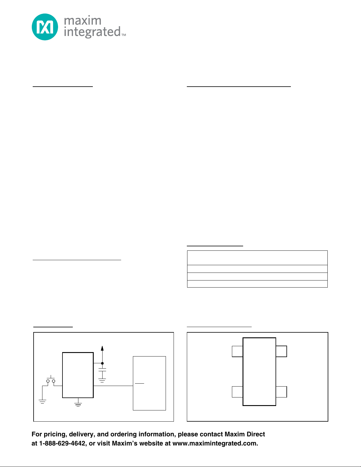
Typical Operating Circuit
MAX6816/MAX6817/MAX6818
V
CC
MECHANICAL
SWITCH
MAX6816
0.1µF
µP
TOP VIEW
GND
1
MAX6816
V
4
CC
GND
OUT
DEBOUNCED
OUTPUT
RESET
IN
OUTIN
2
SOT143
3
Page 2
±15kV ESD-Protected, Single/Dual/Octal,
CMOS Switch Debouncers
ABSOLUTE MAXIMUM RATINGS
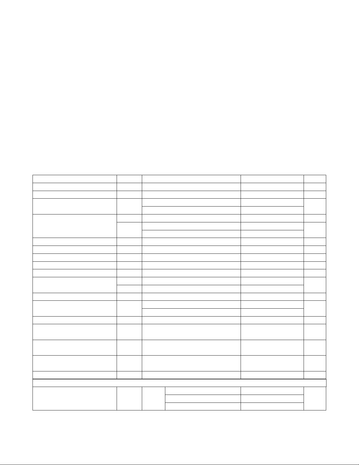
ELECTRICAL CHARACTERISTICS
(VCC= +2.7V to +5.5V, TA= -40°C to +125°C, unless otherwise noted. Typical values are at V
CC
= +5V, TA= +25°C.) (Note 1)
Stresses beyond those listed under “Absolute Maximum Ratings” may cause permanent damage to the device. These are stress ratings only, and functional
operation of the device at these or any other conditions beyond those indicated in the operational sections of the specifications is not implied. Exposure to
absolute maximum rating conditions for extended periods may affect device reliability.
Voltage (with respect to GND)
VCC.......................................................................-0.3V to +6V
IN_ (Switch Inputs) ..............................................-30V to +30V
EN.........................................................................-0.3V to +6V
OUT_, CH ...............................................-0.3V to (V
CC
+ 0.3V)
OUT Short-Circuit Duration
(One or Two Outputs to GND)....................................Continuous
Continuous Power Dissipation (T
A
= +70°C)
4-Pin SOT143 (derate 4.0mW/°C above +70°C)..........320mW
6-Pin SOT23 (derate 8.7mW/°C above +70°C)............691mW
20-Pin SSOP (derate 8.0mW/°C above +70°C) ...........640mW
Operating Temperature Range .........................-40°C to +125°C
Storage Temperature Range .............................-65°C to +160°C
Lead Temperature (soldering, 10s) .................................+300°C
Soldering Temperature (reflow)
Lead(Pb)-free...............................................................+260°C
Containing lead............................................................+240°C
MAX6818
RL= 10kΩ, CL= 50pF
VCC= 5V, I
OUT
= 0A, IN_ = V
CC
RL= 1kΩ, CL = 15pF
RL= 10kΩ, CL= 100pF
VCC= 2.7V
I
SINK
= 1.6mA
VCC= 5V
V
IN
= ±15V
V
CC
= 5V
VCC= 2.7V
I
SOURCE
= 0.4mA
CONDITIONS
ns100t
PC
EN Low to CH Out High
Propagation Delay
ns100t
PD
EN High to Out Three-State
Propagation Delay
ns100t
PE
EN Low to Out Active
Propagation Delay
µA±1I
IL
EN Input Current
0.8 1.1 2.0
0.8 1.7 2.4
ns200t
EN
EN Pulse Width
V
CC
- 1.0V
OH
ms
20 50 80
t
DP
Debounce Duration
µA620I
CC
V2.7 5.5V
CC
Operating Voltage Range
Supply Current
V
0.4V
OL
OUT_, CH Output Voltage
V-25 +25V
IN
Input Voltage Range
mA±1I
IN
IN Input Current
kΩ32 63 100Input Pullup Resistance
V0.8V
IL
V
2.4
V
IH
2.0
mV300Input Hysteresis
UNITSMIN TYP MAXSYMBOLPARAMETER
Input Threshold
V1.9 2.6Undervoltage-Lockout Threshold
V
OUT
= 0V or V
CC
µA±10
OUT_ Three-State Leakage Current
kV
±15
±8
IN_
±15
ESD Protection
V
EN Threshold
IEC 1000-4-2 Air Discharge
IEC 1000-4-2 Contact Discharge
Human Body Model
MAX6816/MAX6817
20 40 60
Note 1: MAX6816 and MAX6817 production testing is done at TA = +25°C; overtemperature limits are guaranteed by design.
ESD CHARACTERISTICS
2
Maxim Integrated
MAX6816/MAX6817/MAX6818
Page 3
±15kV ESD-Protected, Single/Dual/Octal,
CMOS Switch Debouncers
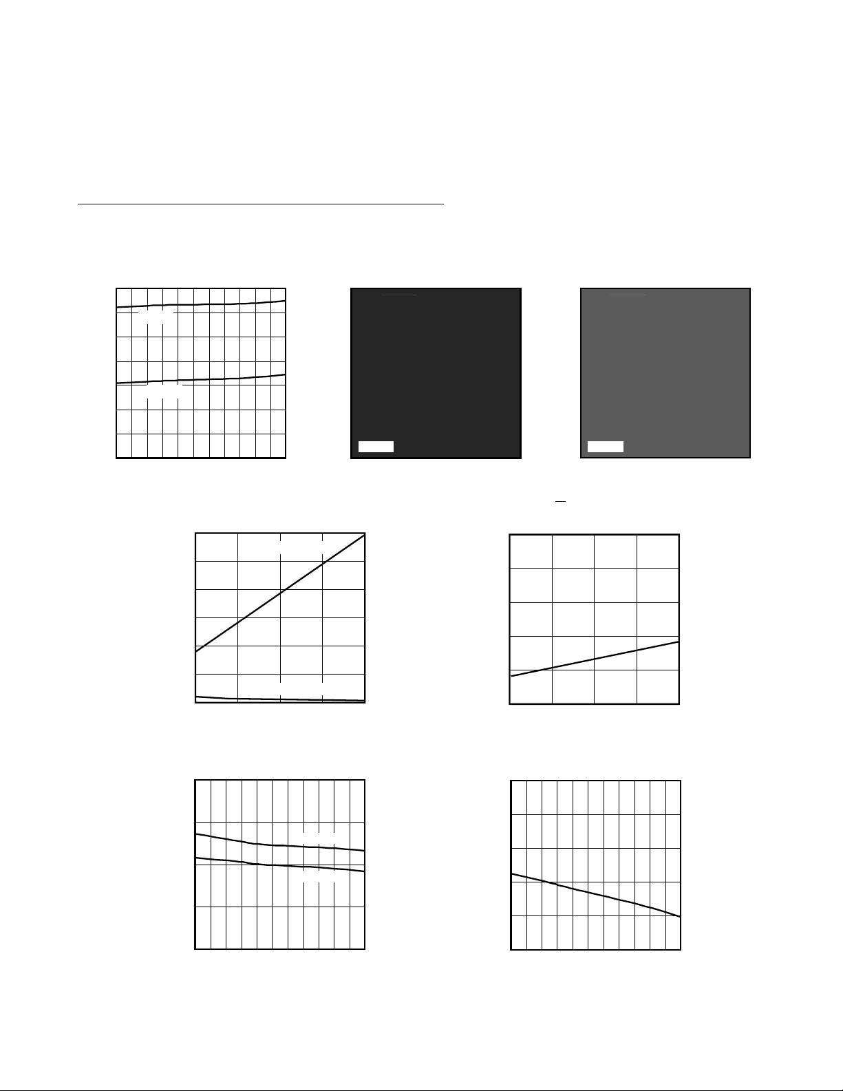
Typical Operating Characteristics
(TA = +25°C, unless otherwise noted.)
Maxim Integrated
3
MAX6816/MAX6817/MAX6818
SUPPLY CURRENT vs. TEMPERATURE
7
6
VCC = 5V
5
4
3
SUPPLY CURRENT (µA)
2
1
0
VCC = 3V
-40 2055035-25 -10 65 80 95 110 125
TEMPERATURE (°C)
OUTPUT LOGIC LEVEL
vs. SUPPLY VOLTAGE
6
5
4
3
2
OUTPUT LOGIC LEVEL (V)
1
0
24356
MAX6816 toc01
VOH, I
SUPPLY VOLTAGE (V)
SOURCE
= 0.4mA
VOL, I
IN (5V/div)OUT (2V/div)
= 1.6mA
SINK
DEBOUNCE OF CLOSING SWITCH
5V
-5V
4V
0V
VCC = 5V
10ms/div
MAX6816 toc04
DEBOUNCE OF OPENING SWITCH
MAX6816 TOC02
5V
IN (5V/div)OUT (2V/div)
-5V
4V
0V
VCC = 5V
10ms/div
MAX6818 EN INPUT LOGIC THRESHOLD
vs. SUPPLY VOLTAGE
5
4
3
2
LOGIC THRESHOLD (V)
1
0
24356
SUPPLY VOLTAGE (V)
MAX6816 toc05
MAX6816 TOC03
DEBOUNCE DELAY PERIOD
vs. TEMPERATURE
50
45
VCC = 5V
40
35
DEBOUNCE DELAY PERIOD (ms)
30
-40 35 50-25 -10 205 95 10065 80
TEMPERATURE (°C)
VCC = 3V
MAX6816 toc06
125
VCC UNDERVOLTAGE LOCKOUT
vs. TEMPERATURE
5
4
3
2
UNDERVOLTAGE LOCKOUT (V)
CC
1
V
0
-40 5035 65 80-25 -10 205 95 100 125
TEMPERATURE (°C)
MAX6816 toc07
Page 4
_______________Detailed Description
Theory of Operation
The MAX6816/MAX6817/MAX6818 are designed to
eliminate the extraneous level changes that result from
interfacing with mechanical switches (switch bounce).
Virtually all mechanical switches bounce upon opening
or closing. These switch debouncers remove bounce
when a switch opens or closes by requiring that
sequentially clocked inputs remain in the same state for
a number of sampling periods. The output does not
change until the input is stable for a duration of 40ms.
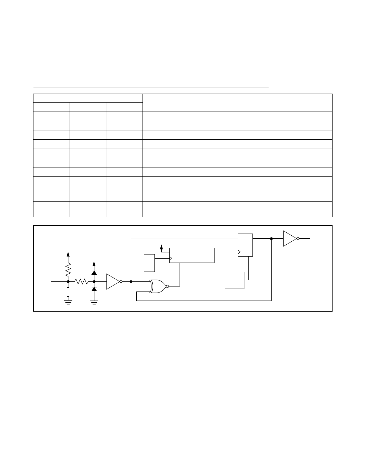
The circuit block diagram (Figure 1) shows the functional blocks consisting of an on-chip oscillator,
counter, exclusive-NOR gate, and D flip-flop. When the
input does not equal the output, the XNOR gate issues
a counter reset. When the switch input state is stable
for the full qualification period, the counter clocks the
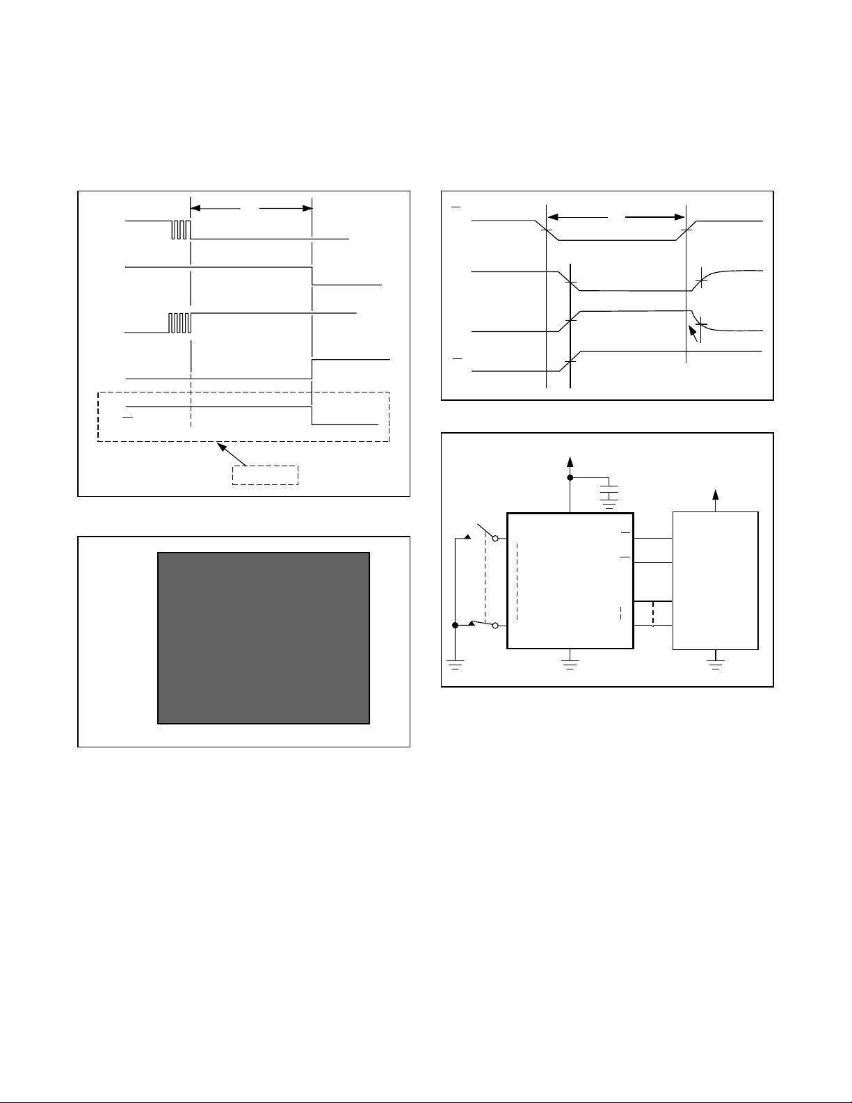
flip-flop, updating the output. Figure 2 shows the typical
opening and closing switch debounce operation. On
the MAX6818, the change output (CH) is updated
simultaneously with the switch outputs.
Undervoltage Lockout
The undervoltage lockout circuitry ensures that the outputs are at the correct state on power-up. While the supply voltage is below the undervoltage threshold
(typically 1.9V), the debounce circuitry remains transparent. Switch states are present at the logic outputs
with no debouce delay.
±15kV ESD-Protected, Single/Dual/Octal,
CMOS Switch Debouncers
PIN
2 — —
— 1, 3 —
— — 12–19
— 4, 6 —
3 — —
— — 2–9
— — 11
— — 1
4 5 20
Pin Description
FUNCTION
Switch Input
Switch Inputs
CMOS Debounced Outputs
CMOS Debounced Outputs
CMOS Debounced Output
Switch Inputs
Change-of-State Output. Goes low on switch input change of
state. Resets on EN. Leave unconnected if not used.
Active-Low, Three-State Enable Input for outputs. Resets CH.
Tie to GND to “always enable” outputs.
+2.7V to +5.5V Supply Voltage
NAME
IN
IN1, IN2
OUT8–OUT1
OUT2, OUT1
OUT
IN1–IN8
CH
EN
V
CC
Figure 1. Block Diagram
1 2 10 GroundGND
MAX6816 MAX6817 MAX6818
4
Maxim Integrated
MAX6816/MAX6817/MAX6818
V
CC
V
CC
R
PU
IN
ESD
PROTECTION
V
CC
OSC.
DQ
R
COUNTER
QD
UNDERVOLTAGE
LOCKOUT
LOAD
MAX6816
MAX6817
MAX6818
OUT
Page 5
Robust Switch Inputs
The switch inputs on the MAX6816/MAX6817/MAX6818
have overvoltage clamping diodes to protect against
damaging fault conditions. Switch input voltages
can safely swing ±25V to ground (Figure 3). Proprietary
ESD-protection structures protect against high
ESD encountered in harsh industrial environments,
membrane keypads, and portable applications.
They are designed to withstand ±15kV per the
IEC 1000-4-2 Air Gap Discharge Test and ±8kV per the
IEC 1000-4-2 Contact Discharge Test.
Since there are 63kΩ (typical) pullup resistors connected to each input, driving an input to -25V will draw
approximately 0.5mA (up to 4mA for eight inputs) from
the V
CC
supply. Driving an input to +25V will cause
approximately 0.32mA of current (up to 2.6mA for eight
inputs) to flow back into the VCCsupply. If the total system V
CC
supply current is less than the current flowing
back into the VCCsupply, VCCwill rise above normal
levels. In some low-current systems, a zener diode on
VCCmay be required.
±15kV ESD Protection
As with all Maxim devices, ESD-protection structures
are incorporated on all pins to protect against electrostatic discharges encountered during handling and
assembly. The MAX6816/MAX6817/MAX6818 have
extra protection against static electricity. Maxim's engineers have developed state-of-the-art structures to protect against ESD of ±15kV at the switch inputs without
±15kV ESD-Protected, Single/Dual/Octal,
CMOS Switch Debouncers
IN1
Figure 2. Input Characteristics
Figure 3. Switch Input ±25V Fault Tolerance
Figure 4. MAX6818 µP-Interface Timing Diagram
Figure 5. MAX6818 Typical µP Interfacing Circuit
Maxim Integrated
5
MAX6816/MAX6817/MAX6818
OUT1
IN2
OUT2
t
DP
EN
OUT1–OUT8
OUT1–OUT8
CH
1
/2 VCC
t
EN
t
PE
t
PE
t
PC
V
1
CC
/2
1
V
/2
CC
1
V
/2
CC
OUT NORMALLY
LOW
OUT NORMALLY
HIGH
1
V
/2
CC
t
PD
V
+ 0.5V
OL
V
- 0.5V
OH
t
PD
CH
MAX6818 ONLY
20V
IN
(20V/div)
0V
-20V
4V
OUT
(2V/div)
0V
20ms/div
+V
CC
+V
CC
µP
IRQ
SW1
IN1
0.1µF
EN I/O
CH
MAX6818
SW8
IN8
OUT1
OUT8
D0
D7
Page 6
±15kV ESD-Protected, Single/Dual/Octal,
CMOS Switch Debouncers
damage. The ESD structures withstand high ESD in all
states: normal operation, shutdown, and powered
down. After an ESD event, the MAX6816/MAX6817/
MAX6818 keep working without latchup, whereas other
solutions can latch and must be powered down to
remove latchup.
ESD protection can be tested in various ways; these
products are characterized for protection to the following limits:
1) ±15kV using the Human Body Model
2) ±8kV using the Contact-Discharge method specified
in IEC 1000-4-2
3) ±15kV using IEC 1000-4-2’s Air-Gap method.
ESD Test Conditions
ESD performance depends on a variety of conditions.
Contact Maxim for a reliability report that documents
test setup, test methodology, and test results.
Human Body Model
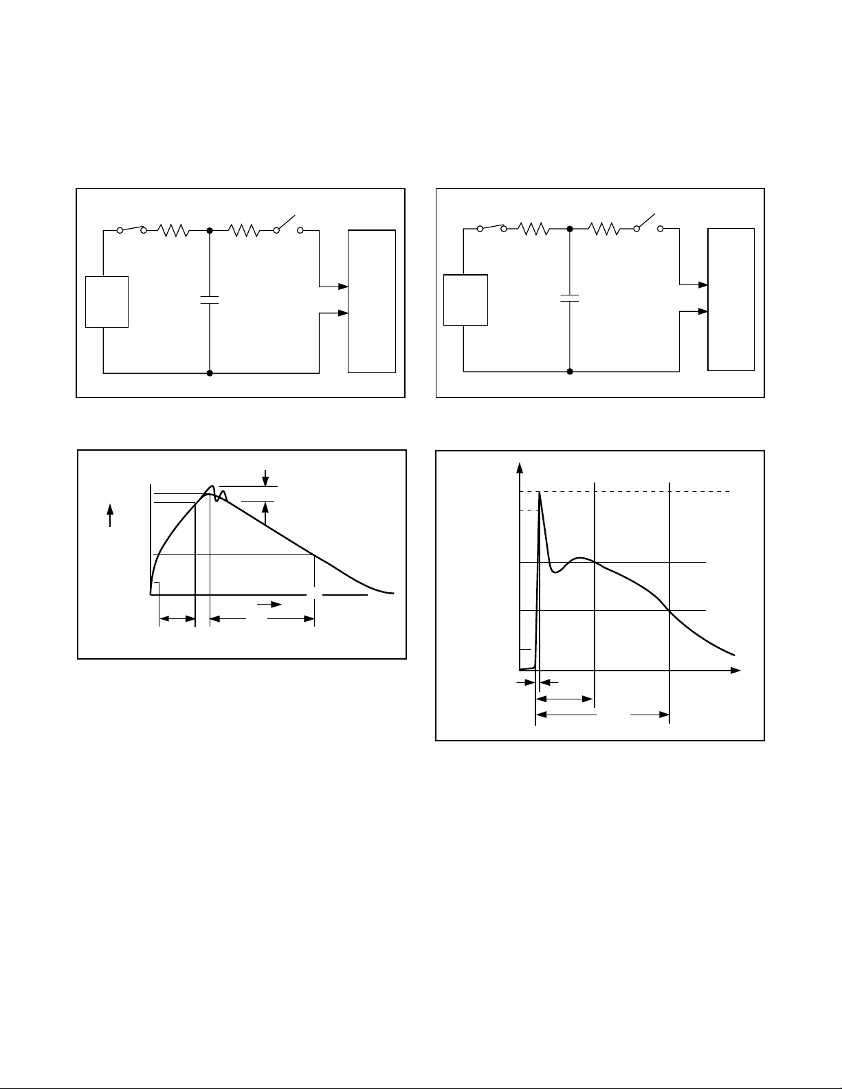
Figure 6a shows the Human Body Model and Figure 6b
shows the current waveform it generates when discharged into a low impedance. This model consists of
a 100pF capacitor charged to the ESD voltage of interest, which is then discharged into the test device
through a 1.5kΩ resistor.
IEC 1000-4-2
The IEC 1000-4-2 standard covers ESD testing and
performance of finished equipment; it does not specifically refer to integrated circuits. The MAX6816/
MAX6817/MAX6818 help you design equipment that
Figure 6b. Human Body Current Waveform
Figure 7b. IEC 1000-4-2 ESD Generator Current Waveform
Figure 6a. Human Body ESD Test Model Figure 7a. IEC 1000-4-2 ESD Test Model
6
Maxim Integrated
MAX6816/MAX6817/MAX6818
50MΩ to 100MΩ RD 330Ω
R
1MΩ RD 1500Ω
R
C
C
DISCHARGE
RESISTANCE
STORAGE
CAPACITOR
HIGH-
VOLTAGE
DC
SOURCE
CHARGE-CURRENT
LIMIT RESISTOR
C
100pF
HIGH-
DC
SOURCE
CHARGE CURRENT
LIMIT RESISTOR
C
150pF
s
DISCHARGE
RESISTANCE
STORAGE
s
CAPACITOR
DEVICE
UNDER
TEST
VOLTAGE
I
PEAK
I
100%
90%
10%
AMPERES
IP 100%
90%
36.8%
10%
PEAK-TO-PEAK RINGING
I
r
(NOT DRAWN TO SCALE)
0
0
t
RL
TIME
t
DL
CURRENT WAVEFORM
DEVICE
UNDER
TEST
tr = 0.7ns to 1ns
30ns
t
60ns
Page 7
±15kV ESD-Protected, Single/Dual/Octal,
CMOS Switch Debouncers
meets Level 4 (the highest level) of IEC 1000-4-2, without the need for additional ESD-protection components.
The major difference between tests done using the
Human Body Model and IEC 1000-4-2 is higher peak
current in IEC 1000-4-2, because series resistance is
lower in the IEC 1000-4-2 model. Hence, the ESD withstand voltage measured to IEC 1000-4-2 is generally
lower than that measured using the Human Body
Model. Figure 7a shows the IEC 1000-4-2 model and
Figure 7b shows the current waveform for the 8kV,
IEC 1000-4-2, Level 4, ESD Contact-Discharge test.
The Air-Gap test involves approaching the device with
a charged probe. The Contact-Discharge method
connects the probe to the device before the probe is
energized.
Machine Model
The Machine Model for ESD tests all pins using a
200pF storage capacitor and zero discharge resistance. Its objective is to emulate the stress caused by
contact that occurs with handling and assembly during
manufacturing.
MAX6818 µP Interfacing
The MAX6818 has an output enable (EN) input that
allows switch outputs to be three-stated on the µP data
bus until polled by the µP. Also, state changes at the
switch inputs are detected, and an output (CH) goes low
after the debounce period to signal the µP. Figure 4
shows the timing diagram for enabling outputs and reading data. If the output enable is not used, tie EN to GND
to “always enable’’ the switch outputs. If EN is low, CH is
always high. If a change of state is not required, leave
CH unconnected.
Pin Configurations (continued)
SUBSTRATE CONNECTED TO GND
PROCESS: BiCMOS
___________________Chip Information
Package Information
For the latest package outline information and land patterns, go
to www.maxim-ic.com/packages
. Note that a “+”, “#”, or “-” in
the package code indicates RoHS status only. Package drawings may show a different suffix character, but the drawing pertains to the package regardless of RoHS status.
PACKAGE
TYPE
PACKAGE
CODE
OUTLINE
NO.
LAND
PATTERN NO.
4 SOT143 U4-1
21-0052 90-0183
6 SOT23 U6-4
21-0058 90-0175
20 SSOP A20-1
21-0056 90-0094
Maxim Integrated
7
MAX6816/MAX6817/MAX6818
TOP VIEW
16OUT1
IN1
GND
MAX6817
2
34
SOT23-6
5 V
CC
OUT2IN2
20
V
CC
19
OUT1
18
OUT2
17
OUT3IN3
16
OUT4
15
OUT5
14
OUT6
13
OUT7IN7
12
OUT8
11
CHGND
IN1
IN2
IN4
IN5
IN6
IN8
1
EN
2
3
4
MAX6818
5
6
7
8
9
10
SSOP
Page 8
±15kV ESD-Protected, Single/Dual/Octal,
CMOS Switch Debouncers
Revision History
MAX6816/MAX6817/MAX6818
8
Maxim Integrated 160 Rio Robles, San Jose, CA 95134 USA 1-408-601-1000
Maxim cannot assume responsibility for use of any circuitry other than circuitry entirely embodied in a Maxim product. No circuit patent licenses are implied.
Maxim reserves the right to change the circuitry and specifications without notice at any time. The parametric values (min and max limits) shown in the Electrical
Characteristics table are guaranteed. Other parametric values quoted in this data sheet are provided for guidance.
©
2010 Maxim Integrated
The Maxim logo and Maxim Integrated are trademarks of Maxim Integrated Products, Inc.
REVISION
NUMBER
0 7/98 Initial release —
3 8/10
REVISION
DATE
DESCRIPTION
Updated Ordering Information, Electrical Characteristics, Typical Operating
Characteristics, and the Undervoltage Lockout section.
PAGES
CHANGED
1–4, 7
 Loading...