

Page 1
General Description
The MAX6697 precision multichannel temperature sensor monitors its own temperature and the temperatures
of up to six external diode-connected transistors. All
temperature channels have programmable alert thresholds. Channels 1, 4, 5, and 6 also have programmable
overtemperature thresholds. When the measured temperature of a channel exceeds the respective threshold, a status bit is set in one of the status registers. Two
open-drain outputs, OVERT and ALERT, assert corresponding to these bits in the status register.
The 2-wire serial interface supports the standard system
management bus (SMBus™) protocols: write byte, read
byte, send byte, and receive byte for reading the temperature data and programming the alarm thresholds.
The MAX6697 is specified for an operating temperature
range of -40°C to +125°C and is available in 20-pin
QSOP and 20-pin TSSOP packages.
Applications
Desktop Computers
Notebook Computers
Workstations
Servers
Features
♦ Six Thermal-Diode Inputs
♦ Local Temperature Sensor
♦ 1°C Remote Temperature Accuracy (+60°C to
+100°C)
♦ Temperature Monitoring Begins at POR for Fail-
Safe System Protection
♦ ALERT and OVERT Outputs for Interrupts,
Throttling, and Shutdown
♦ Small 20-Pin QSOP and 20-Pin TSSOP Packages
♦ 2-Wire SMBus Interface
MAX6697
7-Channel Precision Temperature Monitor
________________________________________________________________ Maxim Integrated Products 1
Ordering Information
20
19
18
17
16
15
14
13
1
2
3
4
5
6
7
8
GND
SMBCLK
SMBDATA
DXN2
DXP2
DXN1
DXP1
V
CC
NC1
NC2DXN4
DXP4
DXN3
DXP3
12
11
9
10
DXP6
DXN6DXN5
DXP5
MAX6697
ALERT
OVERT
2200pF
2200pF
2200pF
2200pF
2200pF
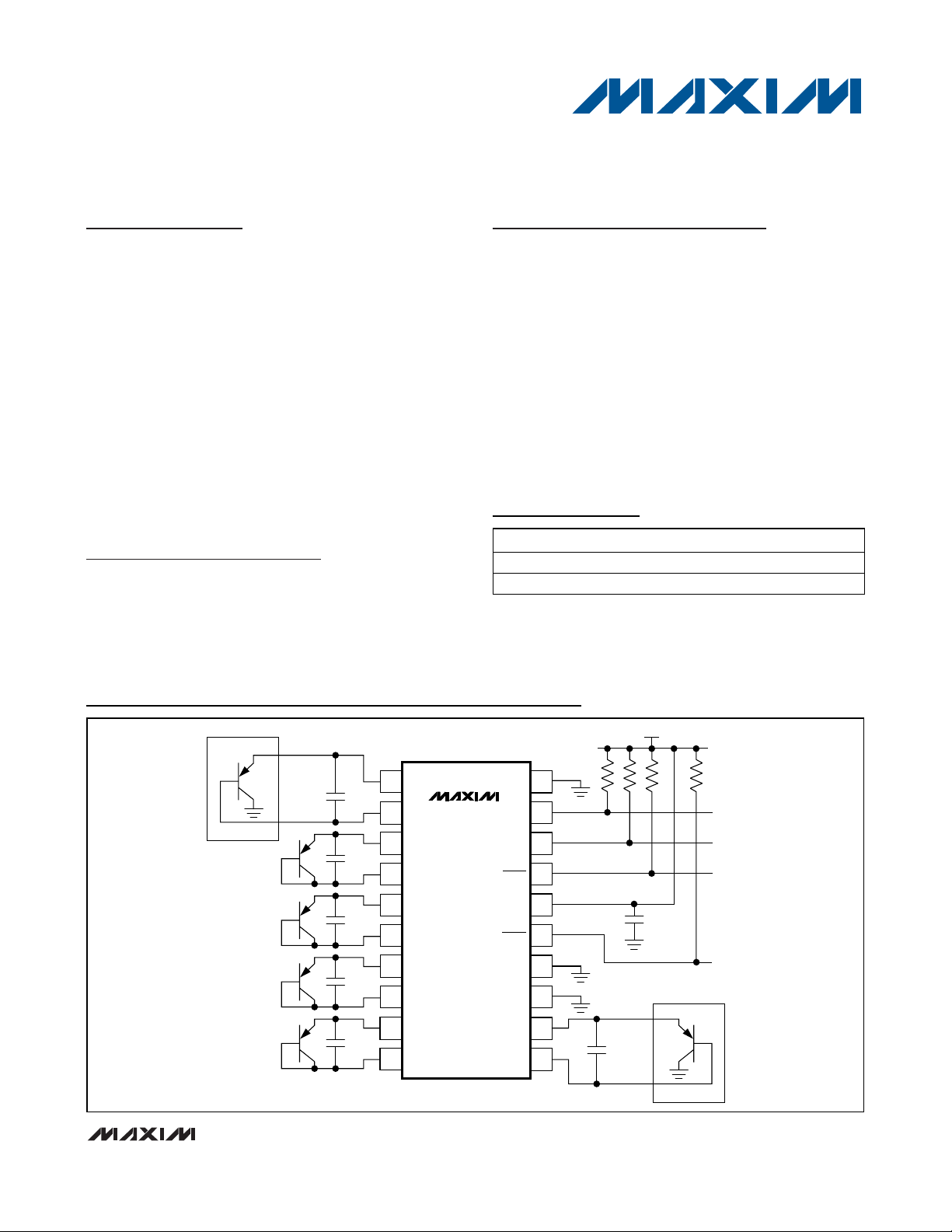
CPU
DXP
DXN
GPU
2200pF
DXN
DXP
0.1μF
TO SYSTEM
SHUTDOWN
INTERRUPT
TO μP
DATA
CLK
4.7kΩ
EACH
+3.3V
Typical Application Circuit
19-3477; Rev 3; 5/09
For pricing, delivery, and ordering information, please contact Maxim Direct at 1-888-629-4642,
or visit Maxim’s website at www.maxim-ic.com.
SMBus is a trademark of Intel Corp.
*See the Slave Address section.
Pin Configuration appears at end of data sheet.
PART TEMP RANGE PIN-PACKAGE
MAX6697EP_ _ -40°C to +125°C
MAX6697UP_ _ -40°C to +125°C
20 QSOP
20 TSSOP
Page 2

MAX6697
7-Channel Precision Temperature Monitor
2 _______________________________________________________________________________________
ABSOLUTE MAXIMUM RATINGS
Stresses beyond those listed under “Absolute Maximum Ratings” may cause permanent damage to the device. These are stress ratings only, and functional
operation of the device at these or any other conditions beyond those indicated in the operational sections of the specifications is not implied. Exposure to
absolute maximum rating conditions for extended periods may affect device reliability.
VCC, SCK, SDA, ALERT, OVERT to GND ................-0.3V to +6V
DXP_ to GND..............................................-0.3V to (V
CC
+ 0.3V)
DXN_ to GND ........................................................-0.3V to +0.8V
SDA, ALERT, OVERT Current .............................-1mA to +50mA
DXN Current .......................................................................±1mA
Continuous Power Dissipation (T
A
= +70°C)
20-Pin QSOP
(derate 9.1mW/°C above +70°C) ......................727.3mW(E20-1)
20-Pin TSSOP
(derate 11.0mW/°C above +70°C)..................879.1mW(U20-2)
ESD Protection (all pins, Human Body Model) ................±2000V
Operating Temperature Range .........................-40°C to +125°C
Junction Temperature......................................................+150°C
Storage Temperature Range .............................-60°C to +150°C
Lead Temperature (soldering, 10s) .................................+300°C
ELECTRICAL CHARACTERISTICS
(VCC= +3.0V to +5.5V, TA= -40°C to +125°C, unless otherwise noted. Typical values are at VCC= +3.3V and TA= +25°C.) (Note 1)
PARAMETER SYMBOL CONDITIONS MIN TYP MAX UNITS
Supply Voltage V
Standby Supply Current I
Operating Current I
Temperature Resolution
Remote Temperature Accuracy VCC = 3.3V
CC
SS
CC
SMBus static 30 µA
During conversion 500 1000 µA
Channel 1 only 11
Other diode channels 8
TA = T
TA = T
= +60°C to +100°C -1.0 +1.0
RJ
= 0°C to +125°C -3.0 +3.0
RJ
DXN_ grounded,
= TA = 0°C to +85°C
T
RJ
Local Temperature Accuracy VCC = 3.3V
TA = +60°C to +100°C -2.0 +2.0
T
= 0°C to +125°C -3.0 +3.0
A
Supply Sensitivity of Temperature
Accuracy
Remote Channel 1 Conversion
Time
Remote Channels 2 Through 6
Conversion Time
Remote-Diode Source Current I
t
CONV1
t
CONV_
RJ
Undervoltage-Lockout Threshold UVLO Falling edge of V
Resistance cancellation on 95 125 156
Resistance cancellation off 190 250 312
High level 80 100 120
Low level 8 10 12
disables ADC 2.30 2.80 2.95 V
CC
Undervoltage-Lockout Hysteresis 90 mV
Power-On Reset (POR) Threshold VCC falling edge 1.2 2.0 2.5 V
POR Threshold Hysteresis 90 mV
ALERT, OVERT
I
= 1mA 0.3
Output Low Voltage V
OL
SINK
I
= 6mA 0.5
SINK
Output Leakage Current 1µA
3.0 5.5 V
±2.5
±0.2
95 125 156 ms
Bits
o
o
o
C/V
ms
µA
C
C
V
Page 3

MAX6697
7-Channel Precision Temperature Monitor
_______________________________________________________________________________________ 3
ELECTRICAL CHARACTERISTICS (continued)
(VCC= +3.0V to +5.5V, TA= -40°C to +125°C, unless otherwise noted. Typical values are at VCC= +3.3V and TA= +25°C.) (Note 1)
Note 1: All parameters are tested at TA= +25°C. Specifications over temperature are guaranteed by design.
Note 2: Timing specifications are guaranteed by design.
Note 3: The serial interface resets when SCL is low for more than t
TIMEOUT
.
Note 4: A transition must internally provide at least a hold time to bridge the undefined region (300ns max) of SCL’s falling edge.
SMBus INTERFACE (SCL, SDA)
Logic-Input Low Voltage V
Logic-Input High Voltage V
Input Leakage Current -1 +1 µA
Output Low Voltage V
Input Capacitance C
SMBus-COMPATIBLE TIMING (Figures 3 and 4) (Note 2)
Serial Clock Frequency f
Bus Free Time Between STOP
and START Condition
START Condition Setup Time
Repeat START Condition Setup
Time
START Condition Hold Time t
STOP Condition Setup Time t
Clock Low Period t
Clock High Period t
Data Hold Time t
Data Setup Time t
Receive SCL/DSA Rise Time t
Receive SCL/SDA Fall Time t
Pulse Width of Spike Suppressed t
SMBus Timeout t
PARAMETER SYMBOL CONDITIONS MIN TYP MAX UNITS
IL
IH
OL
IN
SCL
t
BUF
t
SU:STA
HD:STA
SU:STO
LOW
HIGH
HD:DAT
SU:DAT
R
F
SP
TIMEOUT
VCC = 3.0V 2.2 V
VCC = 5.0V 2.4 V
I
= 6mA 0.3 V
SINK
5pF
(Note 3) 400 kHz
f
= 100kHz 4.7
SCL
f
= 400kHz 1.6
SCL
f
= 100kHz 4.7
SCL
= 400kHz 0.6
f
SCL
90% of SCL to 90% of SDA,
f
= 100kHz
SCL
90% of SCL to 90% of SDA,
f
= 400kHz
SCL
0.6
0.6
10% of SDA to 90% of SCL 0.6 µs
90% of SCL to 90% of SDA,
f
= 100kHz
SCL
90% of SCL to 90% of SDA,
f
= 400kHz
SCL
10% to 10%, f
10% to 10%, f
= 100kHz 1.3
SCL
= 400kHz 1.3
SCL
4
0.6
90% to 90% 0.6 µs
f
= 100kHz 300
SCL
f
= 400kHz (Note 4) 900
SCL
f
= 100kHz 250
SCL
f
= 400kHz 100
SCL
f
= 100kHz 1
SCL
f
= 400kHz 0.3
SCL
050ns
SDA low period for interface reset 25 37 45 ms
0.8 V
µs
µs
µs
µs
µs
ns
ns
µs
300 ns
Page 4
MAX6697
7-Channel Precision Temperature Monitor
4 _______________________________________________________________________________________
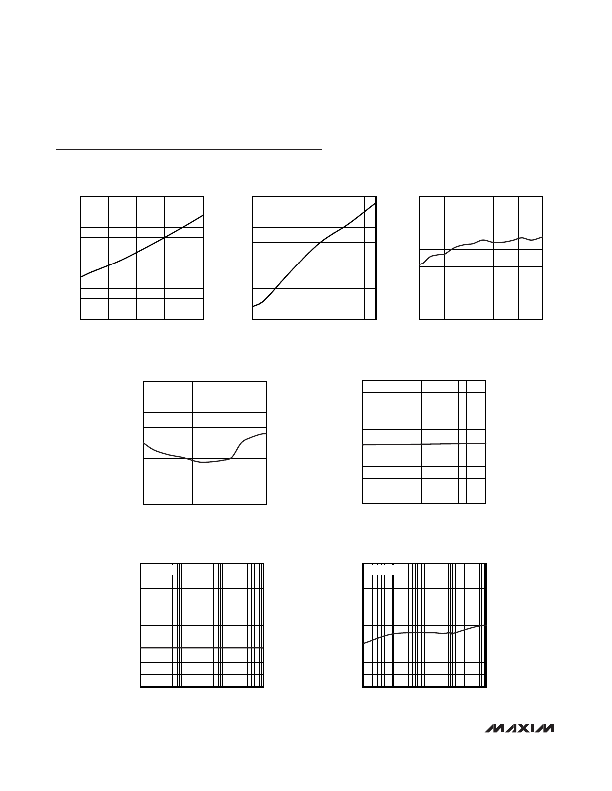
Typical Operating Characteristics
(VCC= 3.3V, TA= +25°C, unless otherwise noted.)
STANDBY SUPPLY CURRENT
vs. SUPPLY VOLTAGE
MAX6697 toc01
SUPPLY VOLTAGE (V)
STANDBY SUPPLY CURRENT (μA)
5.34.84.3
3.8
1
2
3
4
5
6
7
8
9
10
11
12
0
3.3
SUPPLY CURRENT
vs. SUPPLY VOLTAGE
MAX6697 toc02
SUPPLY VOLTAGE (V)
SUPPLY CURRENT (μA)
5.34.8
3.8 4.3
325
330
335
340
350
345
355
360
320
3.3
-4
-2
-3
0
-1
2
1
3
05025 75 100 125
REMOTE TEMPERATURE ERROR
vs. REMOTE-DIODE TEMPERATURE
MAX6697 toc03
REMOTE-DIODE TEMPERATURE (°C)
TEMPERATURE ERROR (°C)
-4
-3
-2
-1
0
1
2
3
4
0 25 50 75 100 125
LOCAL TEMPERATURE ERROR
vs. DIE TEMPERATURE
MAX6697 toc04
DIE TEMPERATURE (°C)
TEMPERATURE ERROR (°C)
REMOTE-DIODE TEMPERATURE ERROR
vs. POWER-SUPPLY NOISE FREQUENCY
MAX6697 toc05
FREQUENCY (MHz)
TEMPERATURE ERROR (°C)
-4
-3
-2
-1
0
1
2
3
4
5
-5
0.1 1
100mV
P-P
LOCAL TEMPERATURE ERROR
vs. POWER-SUPPLY NOISE FREQUENCY
MAX6697 toc06
FREQUENCY (MHz)
TEMPERATURE ERROR (°C)
0.10.01
-4
-3
-2
-1
0
1
2
3
4
5
-5
0.001 1
100mV
P-P
REMOTE TEMPERATURE ERROR
vs. COMMON-MODE NOISE FREQUENCY
MAX6697 toc07
FREQUENCY (MHz)
TEMPERATURE ERROR (°C)
10.10.01
-4
-3
-2
-1
0
1
2
3
4
5
-5
0.001 10
100mV
P-P
Page 5
MAX6697
7-Channel Precision Temperature Monitor
_______________________________________________________________________________________ 5
MAX6697
7-Channel Precision Temperature Monitor
Typical Operating Characteristics (continued)
(VCC= 3.3V, TA= +25°C, unless otherwise noted.)
Pin Description
REMOTE TEMPERATURE ERROR
vs. COMMON-MODE NOISE FREQUENCY
5
100mV
4
3
2
1
0
-1
-2
TEMPERATURE ERROR (°C)
-3
-4
-5
0.001 10
P-P
10.10.01
FREQUENCY (MHz)
MAX6697 toc08
TEMPERATURE ERROR
vs. DXP-DXN CAPACITANCE
0
-0.5
-1.0
-1.5
-2.0
-2.5
-3.0
-3.5
TEMPERATURE ERROR (°C)
-4.0
-4.5
-5.0
1 100
DXP-DXN CAPACITANCE (nF)
10
MAX6697 toc09
PIN NAME FUNCTION
Combined Current Source and A/D Positive Input for Channel 1 Remote Diode. Connect to the anode
1 DXP1
of a remote-diode-connected temperature-sensing transistor. Leave floating or connect to VCC if no
remote diode is used. Place a 2200pF capacitor between DXP1 and DXN1 for noise filtering.
2 DXN1
Cathode Input for Channel 1 Remote Diode. Connect the cathode of the channel 1 remote-diodeconnected transistor to DXN1.
Combined Current Source and A/D Positive Input for Channel 2 Remote Diode. Connect to the anode
3 DXP2
of a remote-diode-connected temperature-sensing transistor. Leave floating or connect to V
remote diode is used. Place a 2200pF capacitor between DXP2 and DXN2 for noise filtering.
4 DXN2
Cathode Input for Channel 2 Remote Diode. Connect the cathode of the channel 2 remote-diodeconnected transistor to DXN2.
Combined Current Source and A/D Positive Input for Channel 3 Remote Diode. Connect to the anode
5 DXP3
of a remote-diode-connected temperature-sensing transistor. Leave floating or connect to VCC if no
remote diode is used. Place a 2200pF capacitor between DXP3 and DXN3 for noise filtering.
6 DXN3
Cathode Input for Channel 3 Remote Diode. Connect the cathode of the channel 1 remote-diodeconnected transistor to DXN3.
Combined Current Source and A/D Positive Input for Channel 4 Remote Diode. Connect to the anode
7 DXP4
of a remote-diode-connected temperature-sensing transistor. Leave floating or connect to V
remote diode is used. Place a 2200pF capacitor between DXP4 and DXN4 for noise filtering.
8 DXN4
Cathode Input for Channel 4 Remote Diode. Connect the cathode of the channel 1 remote-diodeconnected transistor to DXN4.
if no
CC
if no
CC
Page 6

MAX6697
Detailed Description
The MAX6697 is a precision multichannel temperature
monitor that features one local and six remote temperature-sensing channels with a programmable alert
threshold for each temperature channel and a programmable overtemperature threshold for channels 1, 4, 5,
and 6 (see Figure 1). Communication with the MAX6697
is achieved through the SMBus serial interface and a
dedicated alert pin. The alarm outputs, OVERT and
ALERT, assert if the software-programmed temperature
thresholds are exceeded. ALERT typically serves as an
interrupt, while OVERT can be connected to a fan, system shutdown, or other thermal-management circuitry.
ADC Conversion Sequence
In the default conversion mode, the MAX6697 starts the
conversion sequence by measuring the temperature on
channel 1, followed by 2, 3, local channel, 4, 5, and 6.
The conversion result for each active channel is stored
in the corresponding temperature data register.
In some systems, one of the remote thermal diodes may
be monitoring a location that experiences temperature
changes that occur much more rapidly than in the other
channels. If faster temperature changes must be monitored in one of the temperature channels, the MAX6697
allows channel 1 to be monitored at a faster rate than
the other channels. In this mode (set by writing a 1 to bit
4 of the configuration 1 register), measurements of
channel 1 alternate with measurements of the other
channels. The sequence becomes channel 1, channel
2, channel 1, channel 3, channel 1, etc. Note that the
time required to measure all seven channels is considerably greater in this mode than in the default mode.
Low-Power Standby Mode
Standby mode reduces the supply current to less than
15µA by disabling the internal ADC. Enter standby by
setting the STOP bit to 1 in the configuration 1 register.
During standby, data is retained in memory, and the
SMBus interface is active and listening for SMBus commands. The timeout is enabled if a start condition is recognized on SMBus. Activity on the SMBus causes the
supply current to increase. If a standby command is
received while a conversion is in progress, the conversion cycle is interrupted, and the temperature registers
are not updated. The previous data is not changed and
remains available.
7-Channel Precision Temperature Monitor
6 _______________________________________________________________________________________
Pin Description (continued)
PIN NAME FUNCTION
Combined Current Source and A/D Positive Input for Channel 5 Remote Diode. Connect to the anode
9 DXP5
of a remote-diode-connected temperature-sensing transistor. Leave floating or connect to VCC if no
remote diode is used. Place a 2200pF capacitor between DXP5 and DXN5 for noise filtering.
10 DXN5
11 DXN6
12 DXP6
13, 14 NC_ No Connect. Must be connected to ground.
15 OVERT
16 V
17 ALERT
18 SMBDATA SMBus Serial-Data Input/Output. Connect to a pullup resistor.
19 SMBCLK SMBus Serial-Clock Input. Connect to a pullup resistor.
20 GND Ground
CC
Cathode Input for Channel 5 Remote Diode. Connect the cathode of the channel 1 remote-diodeconnected transistor to DXN5.
Cathode Input for Channel 6 Remote Diode. Connect the cathode of the channel 1 remote-diodeconnected transistor to DXN6.
Combined Current Source and A/D Positive Input for Channel 6 Remote Diode. Connect to the anode
of a remote-diode-connected temperature-sensing transistor. Leave floating or connect to V
remote diode is used. Place a 2200pF capacitor between DXP6 and DXN6 for noise filtering.
Overtemperature Active-Low, Open-Drain Output. OVERT asserts low when the temperature of
channels 1, 4, 5, and 6 exceeds the programmed threshold limit.
Supply Voltage Input. Bypass to GND with a 0.1µF capacitor.
SMBus Alert (Interrupt), Active-Low, Open-Drain Output. ALERT asserts low when the temperature of
any channel exceeds the programmed ALERT threshold.
if no
CC
Page 7

SMBus Digital Interface
From a software perspective, the MAX6697 appears as
a series of 8-bit registers that contain temperature measurement data, alarm threshold values, and control bits.
A standard SMBus-compatible 2-wire serial interface is
used to read temperature data and write control bits
and alarm threshold data. The same SMBus slave
address also provides access to all functions.
The MAX6697 employs four standard SMBus protocols:
write byte, read byte, send byte, and receive byte
(Figure 2). The shorter receive byte protocol allows
quicker transfers, provided that the correct data register was previously selected by a read byte instruction.
Use caution with the shorter protocols in multimaster
systems, since a second master could overwrite the
command byte without informing the first master. Figure
3 is the SMBus write timing diagram and Figure 4 is the
SMBus read timing diagram.
The remote diode 1 measurement channel provides 11
bits of data (1 LSB = 0.125°C). All other temperaturemeasurement channels provide 8 bits of temperature
data (1 LSB = 1°C). The 8 most significant bits (MSBs)
can be read from the local temperature and remote
temperature registers. The remaining 3 bits for remote
diode 1 can be read from the extended temperature
register. If extended resolution is desired, the extended
resolution register should be read first. This prevents
the most significant bits from being overwritten by new
MAX6697
7-Channel Precision Temperature Monitor
_______________________________________________________________________________________ 7
Figure 1. Internal Block Diagram
DXP1
DXN1
DXP2
DXN2
DXP3
DXN3
DXP4
DXN4
DXP5
DXN5
DXP6
DXN6
V
CC
10/100μA
INPUT
BUFFER
REF
ADC
SMBus
INTERFACE
COUNT
COUNTER
MAX6697
ALARM
ALU
REGISTER BANK
COMMAND BYTE
REMOTE TEMPERATURES
LOCAL TEMPERATURES
ALERT THRESHOLD
OVERT THRESHOLD
ALERT RESPONSE ADDRESS
OVERT
AVERT
SCL SDA
Page 8

MAX6697
conversion results until they have been read. If the
most significant bits have not been read within an
SMBus timeout period (nominally 37ms), normal updating continues. Table 1 shows the main temperature
register (high byte) data format, and Table 2 shows the
extended resolution register (low byte) data format.
Diode Fault Detection
If a channel’s input DXP_ and DXN_ are left open, the
MAX6697 detects a diode fault. An open diode fault
does not cause either ALERT or OVERT to assert. A bit
in the status register for the corresponding channel is
set to 1 and the temperature data for the channel is
stored as all 1s (FFh). It takes approximately 4ms for
the MAX6697 to detect a diode fault. Once a diode fault
is detected, the MAX6697 goes to the next channel in
7-Channel Precision Temperature Monitor
8 _______________________________________________________________________________________
Write Byte Format
Send Byte Format
Receive Byte Format
Slave Address: equivalent to chip-select line of
a 3-wire interface
Command Byte: selects which
register you are writing to
Data Byte: data goes into the register
set by the command byte (to set
thresholds, configuration masks, and
sampling rate)
Slave Address: equivalent to chip-select line
Command Byte: selects
which register you are
reading from
Slave Address: repeated
due to change in dataflow direction
Data Byte: reads from
the register set by the
command byte
Command Byte: sends command with no data, usually
used for one-shot command
Data Byte: reads data from
the register commanded
by the last read byte or
write byte transmission;
also used for SMBus alert
response return address
S = Start condition Shaded = Slave transmission
P = Stop condition /// = Not acknowledged
S ADDRESS RD ACK DATA /// P
7 bits 8 bits
WRS ACK COMMAND ACK P
8 bits
ADDRESS
7 bits
P
1
ACKDATA
8 bits
ACKCOMMAND
8 bits
ACKWRADDRESS
7 bits
S
S ADDRESS WR ACK COMMAND ACK S ADDRESS
7 bits8 bits7 bits
RD ACK DATA
8 bits
/// P
Figure 2. SMBus Protocols
Table 1. Main Temperature Register
(High Byte) Data Format
Table 2. Extended Resolution Temperature
Register (Low Byte) Data Format
TEMP (°C) DIGITAL OUTPUT
>127 0111 1111
127 0111 1111
126 0111 1110
25 0001 1001
0.00 0000 0000
<0.00 0000 0000
Diode fault (open) 1111 1111
Diode fault (short) 1111 1111 or 1110 1110
TEMP (°C) DIGITAL OUTPUT
0 000X XXXX
+0.125 001X XXXX
+0.250 010X XXXX
+0.375 011X XXXX
+0.500 100X XXXX
+0.625 101X XXXX
+0.725 110X XXXX
+0.875 111X XXXX
Page 9

the conversion sequence. Depending on operating
conditions, a shorted diode may or may not cause
ALERT or OVERT to assert, so if a channel will not be
used, disconnect its DXP and DXN inputs.
Alarm Threshold Registers
There are 11 alarm threshold registers that store overtemperature ALERT and OVERT threshold values.
Seven of these registers are dedicated to store one
local alert temperature threshold limit and six remote
alert temperature threshold limits (see the
ALERT
Interrupt Mode
section). The remaining four registers
are dedicated to remote channels 1, 4, 5, and 6 to store
overtemperature threshold limits (see the
OVERT
Overtemperature Alarm
section). Access to these regis-
ters is provided through the SMBus interface.
ALERT
Interrupt Mode
An ALERT interrupt occurs when the internal or external
temperature reading exceeds a high-temperature limit
(user programmable).The ALERT interrupt output signal
can be cleared by reading the status register(s) associated with the fault(s) or by successfully responding to
an alert response address transmission by the master.
In both cases, the alert is cleared but is reasserted at
the end of the next conversion if the fault condition still
exists. The interrupt does not halt automatic conversions.
The ALERT output is open drain so that multiple devices
MAX6697
7-Channel Precision Temperature Monitor
_______________________________________________________________________________________ 9
Figure 3. SMBus Write Timing Diagram
Figure 4. SMBus Read Timing Diagram
AB CDEFG
t
t
HIGH
LOW
SMBCLK
SMBDATA
t
SU:STAtHD:STA
A = START CONDITION
B = MSB OF ADDRESS CLOCKED INTO SLAVE
C = LSB OF ADDRESS CLOCKED INTO SLAVE
D = R/W BIT CLOCKED INTO SLAVE
AB CDEFG HIJ
t
LOWtHIGH
SMBCLK
SMBDATA
t
t
HD:STA
SU:STA
A = START CONDITION
B = MSB OF ADDRESS CLOCKED INTO SLAVE
C = LSB OF ADDRESS CLOCKED INTO SLAVE
D = R/W BIT CLOCKED INTO SLAVE
E = SLAVE PULLS SMBDATA LINE LOW
t
SU:DAT
E = SLAVE PULLS SMBDATA LINE LOW
F = ACKNOWLEDGE BIT CLOCKED INTO MASTER
G = MSB OF DATA CLOCKED INTO SLAVE
H = LSB OF DATA CLOCKED INTO SLAVE
t
SU:DAT
F = ACKNOWLEDGE BIT CLOCKED INTO MASTER
G = MSB OF DATA CLOCKED INTO MASTER
H = LSB OF DATA CLOCKED INTO MASTER
I = MASTER PULLS DATA LINE LOW
t
HD:DAT
HIJ
I = MASTER PULLS DATA LINE LOW
J = ACKNOWLEDGE CLOCKED INTO SLAVE
K = ACKNOWLEDGE CLOCK PULSE
L = STOP CONDITION
M = NEW START CONDITION
K
J = ACKNOWLEDGE CLOCKED INTO SLAVE
K = ACKNOWLEDGE CLOCK PULSE
L = STOP CONDITION
M = NEW START CONDITION
LMK
t
SU:STOtBUF
L
t
SU:STO
M
t
BUF
Page 10

MAX6697
can share a common interrupt line. All ALERT interrupts
can be masked using the configuration 3 register. The
POR state of these registers is shown in Table 1.
ALERT
Response Address
The SMBus alert response interrupt pointer provides
quick fault identification for simple slave devices that
lack the complex logic needed to be a bus master.
Upon receiving an interrupt signal, the host master can
broadcast a receive byte transmission to the alert
response slave address (see the
Slave Addresses
section). Then, any slave device that generated an interrupt attempts to identify itself by putting its own
address on the bus.
The alert response can activate several different slave
devices simultaneously, similar to the I
2
C General Call.
If more than one slave attempts to respond, bus arbitration rules apply, and the device with the lower address
code wins. The losing device does not generate an
acknowledgment and continues to hold the ALERT line
low until cleared. (The conditions for clearing an alert
vary depending on the type of slave device.)
Successful completion of the alert response protocol
clears the output latch. If the condition that caused the
alert still exists, the MAX6697 reasserts the ALERT
interrupt at the end of the next conversion.
OVERT
Overtemperature Alarms
The MAX6697 has four overtemperature registers that
store remote alarm threshold data for the OVERT output.
OVERT is asserted when a channel’s measured temperature is greater than the value stored in the corresponding threshold register. OVERT remains asserted until the
temperature drops below the programmed threshold
minus 4°C hysteresis. An overtemperature output can
be used to activate a cooling fan, send a warning, initiate clock throttling, or trigger a system shutdown to prevent component damage. See Table 3 for the POR state
of the overtemperature threshold registers.
Command Byte Functions
The 8-bit command byte register (Table 3) is the master
index that points to the various other registers within the
MAX6697. This register’s POR state is 0000 0000.
Configuration Bytes Functions
There are three read-write configuration registers
(Tables 4, 5, and 6) that can be used to control the
MAX6697’s operation.
Configuration 1 Register
The configuration 1 register (Table 4) has several functions. Bit 7(MSB) is used to put the MAX6697 either in
software standby mode (STOP) or continuous conversion mode. Bit 6 resets all registers to their power-on
reset conditions and then clears itself. Bit 5 disables
the SMBus timeout. Bit 4 enables more frequent conversions on channel 1, as described in the
ADC
Conversion Sequence
section. Bit 3 enables resistance
cancellation on channel 1. See the
Series Resistance
Cancellation
section for more details. The remaining
bits of the configuration 1 register are not used. The
POR state of this register is 0000 0000 (00h).
Configuration 2 Register
The configuration 2 register functions are described in
Table 5. Bits [6:0] are used to mask the ALERT interrupt
output. Bit 6 masks the local alert interrupt and bits 5
through bit 0 mask the remote alert interrupts. The
power-up state of this register is 0000 0000 (00h).
Configuration 3 Register
Table 6 describes the configuration 3 register. Bits 5, 4,
3, and 0 mask the OVERT interrupt output for channels
6, 5, 4, and 1. The remaining bits, 7, 6, 2, and 1, are
reserved. The power-up state of this register is 0000
0000 (00h).
Status Registers Functions
Status registers 1, 2, and 3 (Tables 7, 8, and 9) indicate
which (if any) temperature thresholds have been
exceeded and if there is an open-circuit or short-circuit
fault detected with the external sense junctions. Status
register 1 indicates if the measured temperature has
exceeded the threshold limit set in the ALERT registers
for the local or remote-sensing diodes. Status register 2
indicates if the measured temperature has exceeded
the threshold limit set in the OVERT registers. Status
register 3 indicates if there is a diode fault (open or
short) in any of the remote-sensing channels.
Bits in the alert status register clear by a successful
read, but set again after the next conversion unless the
fault is corrected, either by a drop in the measured temperature or an increase in the threshold temperature.
The ALERT interrupt output follows the status flag bit.
Once the ALERT output is asserted, it can be deasserted by either reading status register 1 or by successfully
responding to an alert response address. In both
7-Channel Precision Temperature Monitor
10 ______________________________________________________________________________________
Page 11

MAX6697
7-Channel Precision Temperature Monitor
______________________________________________________________________________________ 11
Table 3. Command Byte Register Bit Assignment
REGISTER
Local 07 00 R Read local temperature register
Remote 1 01 00 R Read channel 1 remote temperature register
Remote 2 02 00 R Read channel 2 remote temperature register
Remote 3 03 00 R Read channel 3 remote temperature register
Remote 4 04 00 R Read channel 4 remote temperature register
Remote 5 05 00 R Read channel 5 remote temperature register
Remote 6 06 00 R Read channel 6 remote temperature register
Configuration 1 41 00 R/W Read/write configuration register 1
Configuration 2 42 00 R/W Read/write configuration register 2
Configuration 3 43 00 R/W Read/write configuration register 3
Status1 44 00 R Read status register 1
Status2 45 00 R Read status register 2
Status3 46 00 R Read status register 3
Local ALERT High Limit 17 5A R/W Read/write local alert high-temperature threshold limit register
Remote 1 ALERT High Limit 11 6E R/W
Remote 2 ALERT High Limit 12 7F R/W
Remote 3 ALERT High Limit 13 64 R/W
Remote 4 ALERT High Limit 14 64 R/W
Remote 5 ALERT High Limit 15 64 R/W
Remote 6 ALERT High Limit 16 64 R/W
Remote 1 OVERT High Limit 21 6E R/W
Remote 4 OVERT High Limit 24 7F R/W
Remote 5 OVERT High Limit 25 5A R/W
Remote 6 OVERT High Limit 26 5A R/W
Remote 1 Extended
Temperature
Manufacturer ID 0A 4D R Read manufacturer ID
ADDRESS
(HEX)
09 00 R Read channel 1 remote-diode extended temperature register
POR STATE
(HEX)
READ/
WRITE
DESCRIPTION
Read/write channel 1 remote-diode alert high-temperature
threshold limit register
Read/write channel 2 remote-diode alert high-temperature
threshold limit register
Read/write channel 3 remote-diode alert high-temperature
threshold limit register
Read/write channel 4 remote-diode alert high-temperature
threshold limit register
Read/write channel 5 remote-diode alert high-temperature
threshold limit register
Read/write channel 6 remote-diode alert high-temperature
threshold limit register
Read/write channel 1 remote-diode overtemperature threshold
limit register
Read/write channel 4 remote-diode overtemperature threshold
limit register
Read/write channel 5 remote-diode overtemperature threshold
limit register
Read/write channel 6 remote-diode overtemperature threshold
limit register
Page 12
MAX6697
cases, the alert is cleared even if the fault condition
exists, but the ALERT output reasserts at the end of the
next conversion. The bits indicating the fault for the
OVERT interrupt output clear only on reading the status
2 register even if the fault conditions still exist. Reading
the status 2 register does not clear the OVERT interrupt
output. To eliminate the fault condition, either the measured temperature must drop below the temperature
threshold minus the hysteresis value (4°C), or the trip
temperature must be set at least 4°C above the current
temperature.
Applications Information
Remote-Diode Selection
The MAX6697 directly measures the die temperature of
CPUs and other ICs that have on-chip temperature-
sensing diodes (see the
Typical Application Circuit
) or
it can measure the temperature of a discrete diodeconnected transistor.
Effect of Ideality Factor
The accuracy of the remote temperature measurements
depends on the ideality factor (n) of the remote “diode”
(actually a transistor). The MAX6697 is optimized for n
= 1.008. A thermal diode on the substrate of an IC is
normally a pnp with the base and emitter brought out
the collector (diode connection) grounded. DXP_ must
be connected to the anode (emitter) and DXN_ must be
connected to the cathode (base) of this pnp. If a sense
transistor with an ideality factor other than 1.008 is
used, the output data is different from the data obtained
with the optimum ideality factor. Fortunately, the difference is predictable. Assume a
7-Channel Precision Temperature Monitor
12 ______________________________________________________________________________________
Table 4. Configuration 1 Register
Table 5. Configuration 2 Register
BIT NAME
7(MSB) STOP 0
6 POR 0
5 TIMEOUT 0 Timeout Enable Bit. Set to logic 0 to enable SMBus timeout.
4 Fast remote 1 0
3
2 Reserved 0 —
1 Reserved 0 —
0 Reserved 0 —
Resistance
cancellation
BIT NAME
7(MSB) Reserved 0
6 Mask Local ALERT 0 Local Alert Mask. Set to logic 1 to mask local channel ALERT.
5 Mask ALERT 6 0 Channel 6 Alert Mask. Set to logic 1 to mask channel 6 ALERT.
4 Mask ALERT 5 0 Channel 5 Alert Interrupt Mask. Set to logic 1 to mask channel 5 ALERT.
3 Mask ALERT 4 0 Channel 4 Alert Mask. Set to logic 1 to mask channel 4 ALERT.
2 Mask ALERT 3 0 Channel 3 Alert Interrupt Mask. Set to logic 1 to mask channel 3 ALERT.
1 Mask ALERT 2 0 Channel 2 Alert Mask. Set to logic 1 to mask channel 2 ALERT.
0 Mask ALERT 1 0 Channel 1 Alert Mask. Set to logic 1 to mask channel 1 ALERT.
POR
STATE
0
POR
STATE
FUNCTION
Standby Mode Control Bit. If STOP is set to logic 1, the MAX6697 stops
converting and enters standby mode.
Reset Bit. Set to logic 1 to put the device into its power-on state. This bit is selfclearing.
Channel 1 Fast Conversion Bit. Set to logic 1 to enable fast conversion of
channel 1.
Resistance Cancellation Bit. When set to logic 1, the MAX6697 cancels series
resistance in the channel 1 thermal diode.
FUNCTION
Page 13

remote-diode sensor designed for a nominal ideality
factor n
NOMINAL
is used to measure the temperature of
a diode with a different ideality factor n1. The measured
temperature TMcan be corrected using:
where temperature is measured in Kelvin and
n
NOMIMAL
for the MAX6697 is 1.008. As an example,
assume you want to use the MAX6697 with a CPU that
has an ideality factor of 1.002. If the diode has no
series resistance, the measured data is related to the
real temperature as follows:
For a real temperature of +85°C (358.15K), the measured temperature is +82.87°C (356.02K), an error of
-2.13°C.
Series Resistance Cancellation
Some thermal diodes on high-power ICs can have
excessive series resistance, which can cause temperature measurement errors with conventional remote temperature sensors. Channel 1 of the MAX6697 has a
series resistance cancellation feature (enabled by bit 3
of the configuration 1 register) that eliminates the effect
of diode series resistance. Set bit 3 to 1 if the series
resistance is large enough to affect the accuracy of
channel 1. The series resistance cancellation function
increases the conversion time for channel 1 by 125ms.
This feature cancels the bulk resistance of the sensor
and any other resistance in series (wire, contact resistance, etc.). The cancellation range is from 0 to 100Ω.
Discrete Remote Diodes
When the remote-sensing diode is a discrete transistor,
its collector and base must be connected together.
Table 10 lists examples of discrete transistors that are
appropriate for use with the MAX6697. The transistor
must be a small-signal type with a relatively high forward voltage; otherwise, the A/D input voltage range
can be violated. The forward voltage at the highest
expected temperature must be greater than 0.25V at
10µA, and at the lowest expected temperature, the forward voltage must be less than 0.95V at 100µA. Large
power transistors must not be used. Also, ensure that
the base resistance is less than 100Ω. Tight specifications for forward current gain (50 < ß <150, for example) indicate that the manufacturer has good process
controls and that the devices have consistent VBEcharacteristics. Manufacturers of discrete transistors do not
normally specify or guarantee ideality factor. This is
normally not a problem since good-quality discrete
transistors tend to have ideality factors that fall within a
relatively narrow range. We have observed variations in
remote temperature readings of less than ±2°C with a
variety of discrete transistors. Still, it is good design
practice to verify good consistency of temperature
readings with several discrete transistors from any
manufacturer under consideration.
MAX6697
7-Channel Precision Temperature Monitor
______________________________________________________________________________________ 13
Table 6. Configuration 3 Register
n
1
1 008
⎛
⎜
⎝
1 002
.
.
POR
STATE
⎞
⎟
⎠
⎞
=
⎟
⎠
Channel 6 Remote-Diode OVERT Mask Bit. Set to logic 1 to mask channel 6
OVERT.
Channel 5 Remote-Diode OVERT Mask Bit. Set to logic 1 to mask channel 5
OVERT.
Channel 4 Remote-Diode OVERT Mask Bit. Set to logic 1 to mask channel 4
OVERT.
Channel 1 Remote-Diode OVERT Mask Bit. Set to logic 1 to mask channel 1
OVERT.
1 00599
(. )
BIT NAME
7(MSB) Reserved 0 —
6 Reserved 0 —
5 Mask OVERT 6 0
4 Mask OVERT 5 0
3 Mask OVERT 4 0
2 Reserved 0 —
1 Reserved 0 —
0 Mask OVERT 1 0
TT
=
M ACTUAL
⎛
⎜
n
⎝
NOMINAL
⎛
n
TT
ACTUAL M
=×
NOMINAL
⎜
⎝
⎞
TT
=×
MM
⎟
n
⎠
1
FUNCTION
Page 14

MAX6697
Unused Diode Channels
If one or more of the remote diode channels is not
needed, the DXP and DXN inputs for that channel
should either be unconnected, or the DXP input should
be connected to VCC. The status register indicates a
diode "fault" for this channel and the channel is ignored
during the temperature-measurement sequence. It is
also good practice to mask any unused channels
immediately upon power-up by setting the appropriate
bits in the Configuration 2 and Configuration 3 registers. This will prevent unused channels from causing
ALERT# or OVERT# to assert.
Thermal Mass and Self-Heating
When sensing local temperature, the MAX6697 measures the temperature of the printed-circuit board
(PCB) to which it is soldered. The leads provide a good
thermal path between the PCB traces and the die. As
with all IC temperature sensors, thermal conductivity
between the die and the ambient air is poor by compar-
ison, making air temperature measurements impractical. Because the thermal mass of the PCB is far greater
than that of the MAX6697, the device follows temperature changes on the PCB with little or no perceivable
delay. When measuring the temperature of a CPU or
other IC with an on-chip sense junction, thermal mass
has virtually no effect; the measured temperature of the
junction tracks the actual temperature within a conversion cycle.
When measuring temperature with discrete remote
transistors, the best thermal response times are
obtained with transistors in small packages (i.e., SOT23
or SC70). Take care to account for thermal gradients
between the heat source and the sensor, and ensure
that stray air currents across the sensor package do
not interfere with measurement accuracy. Self-heating
does not significantly affect measurement accuracy.
Remote-sensor self-heating due to the diode current
source is negligible.
7-Channel Precision Temperature Monitor
14 ______________________________________________________________________________________
Table 7. Status 1 Register
BIT NAME
7(MSB) Reserved 0 —
6 Local ALERT 0
5 Remote 6 ALERT 0
4 Remote 5 ALERT 0
3 Remote 4 ALERT 0
2 Remote 3 ALERT 0
POR
STATE
Local Channel High-Alert Bit. This bit is set to logic 1 when the local
temperature exceeds the temperature threshold limit in the local ALERT highlimit register.
Channel 6 Remote-Diode High-Alert Bit. This bit is set to logic 1 when the
channel 6 remote-diode temperature exceeds the temperature threshold limit
in the remote 6 ALERT high-limit register.
Channel 5 Remote-Diode High-Alert Bit. This bit is set to logic 1 when the
channel 5 remote-diode temperature exceeds the programmed temperature
threshold limit in the remote 5 ALERT high-limit register.
Channel 4 Remote-Diode High-Alert Bit. This bit is set to logic 1 when the
channel 4 remote-diode temperature exceeds the temperature threshold limit
in the remote 4 ALERT high-limit register.
Channel 3 Remote-Diode High-Alert Bit. This bit is set to logic 1 when the
channel 3 remote-diode temperature exceeds the programmed temperature
threshold limit in the remote 3 ALERT high-limit register.
FUNCTION
Channel 2 Remote-Diode High-Alert Bit. This bit is set to logic 1 when the
1 Remote 2 ALERT 0
0 Remote 1 ALERT 0
channel 2 remote-diode temperature exceeds the temperature threshold limit
in the remote 2 ALERT high-limit register.
Channel 1 Remote-Diode High-Alert Bit. This bit is set to logic 1 when the
channel 1 remote-diode temperature exceeds the temperature threshold limit
in the remote 1 ALERT high-limit register.
Page 15

MAX6697
7-Channel Precision Temperature Monitor
______________________________________________________________________________________ 15
Table 8. Status 2 Register
Table 9. Status 3 Register
BIT NAME
7(MSB) Reserved 0 —
6 Reserved 0 —
5 Remote 6 OVERT 0
4 Remote 5 OVERT 0
3 Remote 4 OVERT 0
2 Reserved 0 —
1 Reserved 0 —
0 Remote 1 OVERT 0
POR
STATE
BIT NAME
7(MSB) Reserved 0 —
6 Diode fault 6 0
5 Diode fault 5 0
4 Diode fault 4 0
3 Diode fault 3 0
2 Diode fault 2 0
1 Diode fault 1 0
0 Reserved 0 —
POR
STATE
FUNCTION
Channel 6 Remote-Diode Overtemperature Status Bit. This bit is set to logic 1
when the channel 6 remote-diode temperature exceeds the temperature
threshold limit in the remote 6 OVERT high-limit register.
Channel 5 Remote Diode Overtemperature Status Bit. This bit is set to logic 1
when the channel 5 remote-diode temperature exceeds the temperature
threshold limit in the remote 5 OVERT high-limit register.
Channel 4 Remote Diode Overtemperature Status Bit. This bit is set to logic 1
when the channel 4 remote-diode temperature exceeds the temperature
threshold limit in the remote 4 OVERT high-limit register.
Channel 1 Remote-Diode Overtemperature Status Bit. This bit is set to logic 1
when the channel 1 remote-diode temperature exceeds the temperature
threshold limit in the remote 1 OVERT high-limit register.
FUNCTION
Channel 6 Remote-Diode Fault Bit. This bit is set to 1 when DXP6 and DXN6
are open circuit or when DXP6 is connected to V
Channel 5 Remote-Diode Fault Bit. This bit is set to 1 when DXP5 and DXN5
are open circuit or when DXP5 is connected to V
Channel 4 Remote-Diode Fault Bit. This bit is set to 1 when DXP4 and DXN4
are open circuit or when DXP4 is connected to V
Channel 3 Remote-Diode Fault Bit. This bit is set to 1 when DXP3 and DXN3
are open circuit or when DXP3 is connected to V
Channel 2 Remote-Diode Fault Bit. This bit is set to 1 when DXP2 and DXN2
are open circuit or when DXP2 is connected to V
Channel 1 Remote-Diode Fault Bit. This bit is set to 1 when DXP1 and DXN1
are open circuit or when DXP1 is connected to V
CC
CC
CC
CC
CC
CC
.
.
.
.
.
.
Page 16

MAX6697
Slave Address
Table 11 shows the MAX6697 slave addresses.
ADC Noise Filtering
The integrating ADC has good noise rejection for lowfrequency signals such as power-supply hum. In environments with significant high-frequency EMI, connect
an external 2200pF capacitor between DXP_ and
DXN_. Larger capacitor values can be used for added
filtering, but do not exceed 3300pF because it can
introduce errors due to the rise time of the switched
current source. High-frequency noise reduction is
needed for high-accuracy remote measurements.
Noise can be reduced with careful PCB layout as discussed in the
PCB Layout
section.
PCB Layout
Follow these guidelines to reduce the measurement
error when measuring remote temperature:
1) Place the MAX6697 as close as is practical to the
remote diode. In noisy environments, such as a
computer motherboard, this distance can be 4in to
8in (typ). This length can be increased if the worst
noise sources are avoided. Noise sources include
CRTs, clock generators, memory buses, and PCI
buses.
2) Do not route the DXP-DXN lines next to the deflection coils of a CRT. Also, do not route the traces
across fast digital signals, which can easily introduce +30°C error, even with good filtering.
3) Route the DXP and DXN traces in parallel and in
close proximity to each other. Each parallel pair of
traces should go to a remote diode. Route these
traces away from any higher voltage traces, such as
+12VDC. Leakage currents from PCB contamination
must be dealt with carefully since a 20MΩ leakage
path from DXP to ground causes about +1°C error.
If high-voltage traces are unavoidable, connect
guard traces to GND on either side of the DXP-DXN
traces (Figure 5).
4) Route through as few vias and crossunders as possible to minimize copper/solder thermocouple
effects.
5) Use wide traces when practical.
6) When the power supply is noisy, add a resistor (up
to 47Ω) in series with V
CC
.
7-Channel Precision Temperature Monitor
16 ______________________________________________________________________________________
Figure 5. Recommended DXP-DXN PCB Traces
Table 10. Remote-Sensors Transistor
Manufacturer
Note: Discrete transistors must be diode connected (base
shorted to collector).
Table 11. Slave Address
MANUFACTURER MODEL NO.
Central Semiconductor (USA) CMPT3904
Rohm Semiconductor (USA) SST3904
Samsung (Korea) KST3904-TF
Siemens (Germany) SMBT3904
Zetex (England) FMMT3904CT-ND
PART SMBus SLAVE ID PIN-PACKAGE
MAX6697EP34 0011 010 20 QSOP
MAX6697EP38 0011 100 20 QSOP
MAX6697EP99 1001 100 20 QSOP
MAX6697EP9C 1001 110 20 QSOP
MAX6697UP34 0011 010 20 TSSOP
MAX6697UP38 0011 100 20 TSSOP
MAX6697UP99 1001 100 20 TSSOP
MAX6697UP9C 1001 110 20 TSSOP
10 mils
10 mils
GND
DXP
DXN
GND
10 mils
MINIMUM
10 mils
Page 17

Twisted-Pair and Shielded Cables
Use a twisted-pair cable to connect the remote sensor
for remote-sensor distances longer than 8in or in very
noisy environments. Twisted-pair cable lengths can be
between 6ft and 12ft before noise introduces excessive
errors. For longer distances, the best solution is a
shielded twisted pair like that used for audio microphones. For example, Belden #8451 works well for distances up to 100ft in a noisy environment. At the
device, connect the twisted pair to DXP and DXN and
the shield to GND. Leave the shield unconnected at the
remote sensor. For very long cable runs, the cable’s
parasitic capacitance often provides noise filtering, so
the 2200pF capacitor can often be removed or reduced
in value. Cable resistance also affects remote-sensor
accuracy. For every 1Ω of series resistance the error is
approximately +1/2°C.
MAX6697
7-Channel Precision Temperature Monitor
______________________________________________________________________________________ 17
Pin Configuration
Chip Information
PROCESS: BiCMOS
Package Information
For the latest package outline information and land patterns, go
to www.maxim-ic.com/packages
. Note that a “+”, “#”, or “-” in
the package code indicates RoHS status only. Package drawings may show a different suffix character, but the drawing pertains to the package regardless of RoHS status.
PACKAGE TYPE PACKAGE CODE DOCUMENT NO.
20 QSOP E20-1
21-0055
20 TSSOP U20-2
21-0066
TOP VIEW
DXP1
DXN1
DXP2
DXN2
DXP3
DXN3
DXP4
DXP5
1
2
3
4
MAX6697
5
6
7
8
9
10
QSOP/TSSOP
20
19
18
17
16
15
14
13
12
11
GND
SMBCLK
SMBDATA
ALERT
V
CC
OVERT
NC1
NC2DXN4
DXP6
DXN6DXN5
Page 18

MAX6697
7-Channel Precision Temperature Monitor
Maxim cannot assume responsibility for use of any circuitry other than circuitry entirely embodied in a Maxim product. No circuit patent licenses are
implied. Maxim reserves the right to change the circuitry and specifications without notice at any time.
18
____________________Maxim Integrated Products, 120 San Gabriel Drive, Sunnyvale, CA 94086 408-737-7600
© 2009 Maxim Integrated Products Maxim is a registered trademark of Maxim Integrated Products Inc.
MAX6697
Revision History
REVISION
NUMBER
3 5/09 Corrected remote sensor connections in Typical Application Circuit 1
REVISION
DATE
DESCRIPTION
PAGES
CHANGED
 Loading...