

Page 1
General Description
The MAX6604 high-precision temperature sensor is
designed for thermal monitoring functions in DDR memory modules. The device is readable and programmable
through the 2-wire SMBus™/I2C-compatible interface.
Three address inputs set the bus address for the temperature sensor to provide up to eight devices on one bus.
The internal thermal sensor continuously monitors the
temperature and updates the temperature data eight
times per second. The master can read the temperature data at any time. Since the thermal sensor is located on the memory module, temperature data recorded
accurately represents the temperature of the components on the module. Consequently, the MAX6604 provides a much more accurate measurement of module
temperature than techniques involving temperature
sensors on the motherboard. In addition, the device
responds more quickly to temperature changes on the
module than a motherboard sensor.
The MAX6604 also features an interrupt-output indicator for temperature-threshold monitoring. The threshold
levels are programmable through the digital interface.
The MAX6604 operates from -20°C to +125°C, and is
available in JEDEC-standard 8-pin TSSOP and TDFN
(MO-229-WCED-2) packages.
Applications
Memory Modules
Desktop Computers
Notebook Computers
Workstations
Networking Equipment
Features
♦ JEDEC Compliant
♦ ±1°C Temperature-Monitoring Accuracy
♦ Overtemperature Interrupt with Programmable
Threshold
♦ +2.7V to +3.6V Operating Voltage Range
♦ SMBus/I2C-Compatible Interface
♦ 300µA Typical Operating Current
♦ 3µA Typical Shutdown Current
♦ -20°C to +125°C Operating Temperature Range
♦ 8-Pin TSSOP and TDFN (MO-229-WCED-2)
Packages
MAX6604
Precision Temperature Monitor for
DDR Memory Modules
________________________________________________________________ Maxim Integrated Products 1
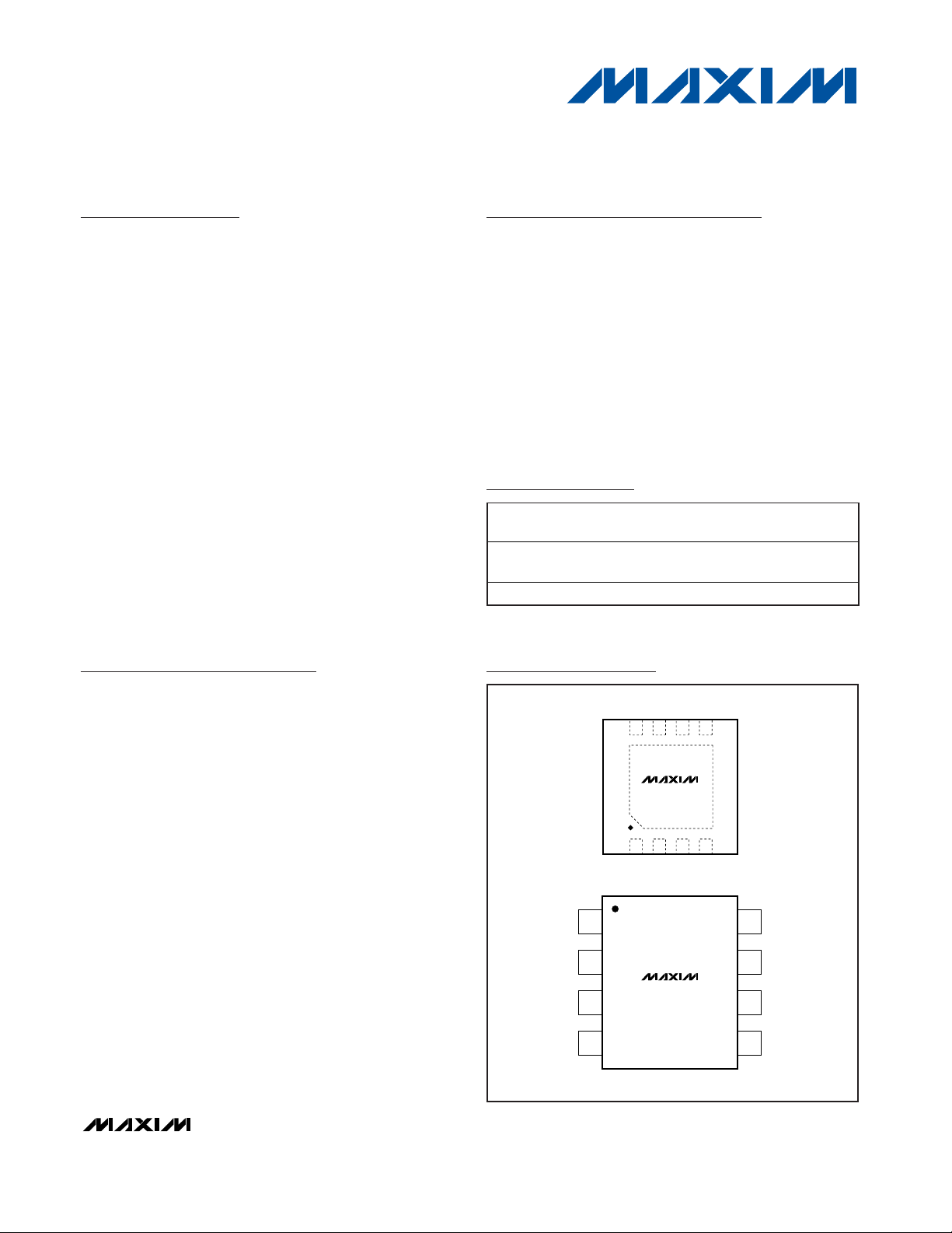
Ordering Information
19-3837; Rev 0; 10/05
For pricing, delivery, and ordering information, please contact Maxim/Dallas Direct! at
1-888-629-4642, or visit Maxim’s website at www.maxim-ic.com.
PART
PIN-PACKAGE
PKG
CODE
MAX6604ATA
8 TDFN-EP**
T823-1
MAX6604AHA
8 TSSOP H8-1
SMBus is a trademark of Intel Corporation.
Typical Application Circuit appears at end of data sheet.
134
865
V
CC
SCL SDA
MAX6604
MAX6604
2
7
EVENT
A0 A2 GNDA1
TDFN-EP**
TSSOP
TOP VIEW
SCL
SDA
GND
1
2
8
7
V
CC
EVENT
A1
A2A03
4
6
5
Pin Configurations
**EP = Exposed paddle.
TEMP RANGE
-20°C to +125°C
-20°C to +125°C
(MO229-WCED-2)
Page 2

MAX6604
Precision Temperature Monitor for
DDR Memory Modules
2 _______________________________________________________________________________________
ABSOLUTE MAXIMUM RATINGS
ELECTRICAL CHARACTERISTICS
(VCC= +2.7V to +3.6V, TA= -20°C to +125°C, unless otherwise noted. Typical values are at VCC= +3.3V, TA= +25°C.) (Note 1)
Stresses beyond those listed under “Absolute Maximum Ratings” may cause permanent damage to the device. These are stress ratings only, and functional
operation of the device at these or any other conditions beyond those indicated in the operational sections of the specifications is not implied. Exposure to
absolute maximum rating conditions for extended periods may affect device reliability.
All Input and Output Voltages ..................................-0.3V to +6V
Continuous Power Dissipation (TA= +70°C)
8-Pin TDFN (derate 16.7mW/°C above +70°C) ......1333.3mW
8-Pin TSSOP (derate 8.1mW/°C above +70°C) ........646.7mW
ESD Protection (all pins, Human Body Model) ....................±2kV
Junction Temperature......................................................+150°C
Operating Temperature Range .........................-20°C to +125°C
Storage Temperature Range .............................-65°C to +150°C
Lead Temperature (soldering, 10s) .................................+300°C
PARAMETER
SYMBOL
CONDITIONS
MIN
TYP
MAX
UNITS
Operating Supply Voltage Range V
CC
V
°C
Temperature Resolution
11 bits
+3V ≤ VCC ≤ +3.6V, +75°C ≤ TA ≤ +95°C -1 +1
-2 +2
Temperature Accuracy
+3V ≤ V
CC
≤ +3.6V, -20°C ≤ TA ≤ +125°C -3 +3
°C
Power-On Reset (POR) Threshold VCC falling edge 2.0 V
POR Threshold Hysteresis 90 mV
Undervoltage-Lockout Threshold 2.4 V
Operating Current During conversion 0.3 0.5 mA
Standby Current 36µA
Conversion Time
125 ms
Conversion Rate
8Hz
DIGITAL INTERFACE (Note 2)
Log i c- Inp ut H i g h V ol tag e ( S C L, S D A)
V
IH
2.1 V
Logic-Input Low Voltage (SCL, SDA)
V
IL
0.8 V
Logic-Input Hysteresis (SCL, SDA) 500 mV
Leakag e C ur r ent ( E V E N T, S C L, S D A,
A2, A1, A0)
I
LEAK
V
IN
= GND or V
CC
-1 +1 µA
Logic-Output Low Voltage
(SDA, EVENT)
V
OL
I
PULL_UP
= 350µA 50 mV
Logic-Output Low Sink Current
(SDA, EVENT)
I
OL
VOL = 0.6V 6 mA
Input Capacitance (SCL, SDA) C
IN
5pF
Serial-Clock Frequency f
SCL
10 100 kHz
+2.7 +3.6
0.125
+3V ≤ V
t
CONV
f
CONV
≤ +3.6V, +40°C ≤ TA ≤ +125°C
CC
Page 3

MAX6604
Precision Temperature Monitor for
DDR Memory Modules
_______________________________________________________________________________________ 3
ELECTRICAL CHARACTERISTICS (continued)
(VCC= +2.7V to +3.6V, TA= -20°C to +125°C, unless otherwise noted. Typical values are at VCC= +3.3V, TA= +25°C.) (Note 1)
PARAMETER
SYMBOL
CONDITIONS
MIN
TYP
MAX
UNITS
Bus Free Time Between STOP and
START Condition
t
BUF
4.7 µs
90% to 90% 4.7 µs
START Condition Hold Time
10% of SMBDATA to 90% of SMBCLK 4 µs
STOP Condition Setup Time
90% of SMBCLK to 10% of SMBDATA 4 µs
Clock Low Period t
LOW
10% to 10% 4.7 µs
Clock High Period t
HIGH
90% to 90% 4 µs
Data Hold Time
300 ns
Data Setup Time
90% of SMBDATA to 10% of SMBCLK 250 ns
Receive SCL/SDA Rise Time t
R
ns
Receive SCL/SDA Fall Time t
F
300 ns
Pulse Width of Spike Suppressed t
SP
050ns
Note 1: All parameters are tested at TA= +25°C. Specifications over temperature are guaranteed by design.
Note 2: Guaranteed by design.
Rep eat S TART C ond i ti on S etup Ti m et
SU:STA
t
HD:STA
t
SU:STO
t
HD:DAT
t
SU:DAT
1000
Page 4
MAX6604
Precision Temperature Monitor for
DDR Memory Modules
4 _______________________________________________________________________________________
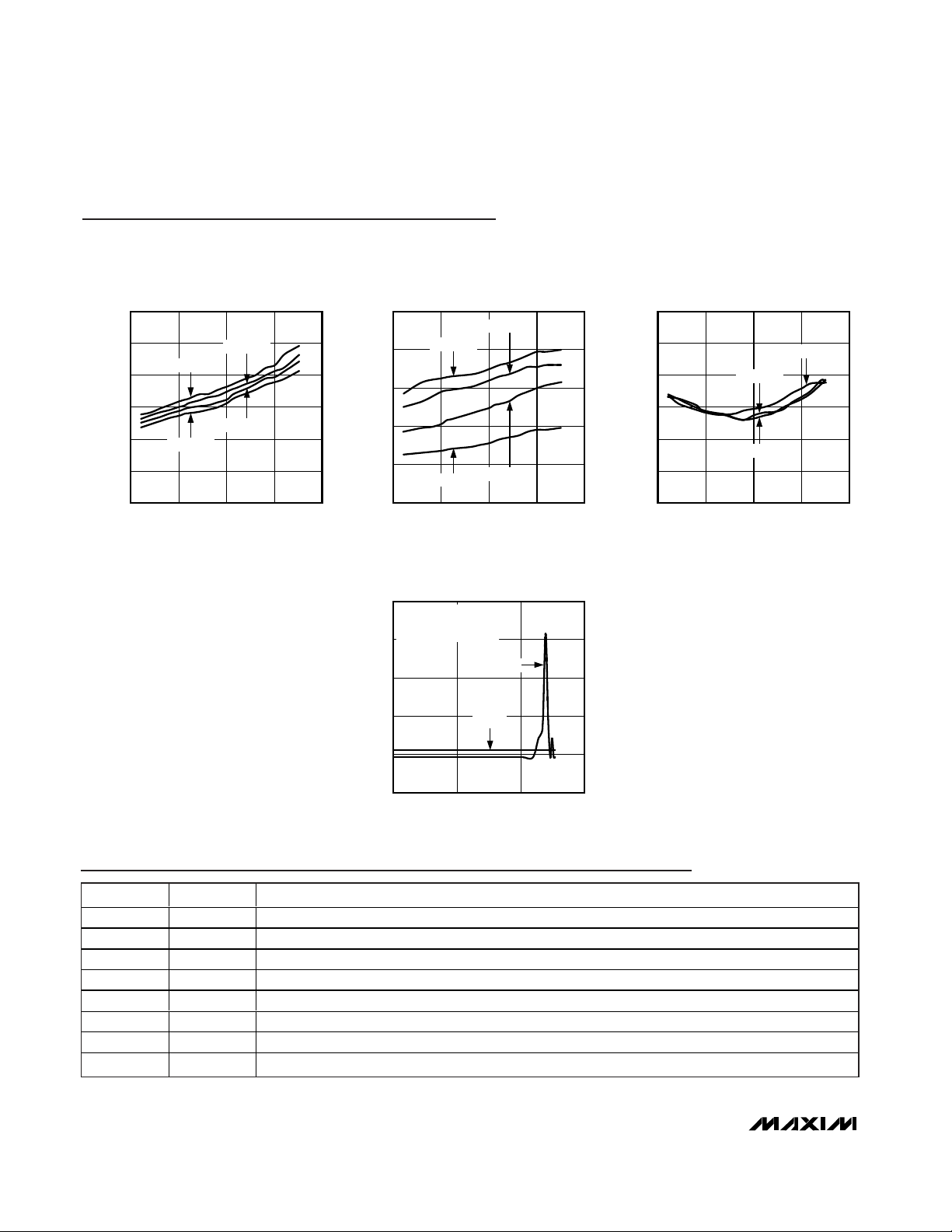
Typical Operating Characteristics
(Typical values are at VCC= +3.3V, TA= +25°C.)
0
2
1
4
3
5
6
-50 150
SHUTDOWN SUPPLY CURRENT
vs. TEMPERATURE
MAX6604 toc01
TEMPERATURE (°C)
SHUTDOWN SUPPLY CURRENT (µA)
0 50 100
VCC = 3.6V
VCC = 2.7V
VCC = 3.3V
VCC = 3.0V
340
360
320
300
280
260
-50 150
SUPPLY CURRENT
vs. TEMPERATURE
MAX6604 toc02
TEMPERATURE (°C)
SUPPLY CURRENT (µA)
0 50 100
VCC = 3.6V
VCC = 2.7V
VCC = 3.3V
VCC = 3.0V
-3
-1
-2
1
0
2
3
-50 150
TEMPERATURE ERROR
vs. TEMPERATURE
MAX6604 toc03
TEMPERATURE (°C)
TEMPERATURE ERROR (°C)
050100
VCC = 3.0V
VCC = 3.3V
VCC = 3.6V
2.5
2.0
1.5
1.0
0.5
0
0.1 100,000
TEMPERATURE ERROR
vs. POWER SUPPLY NOISE FREQUENCY
MAX6604 toc04
POWER SUPPLY NOISE FREQUENCY (kHz)
TEMPERATURE ERROR (°C)
10 1,000
SQUARE WAVE APPLIED
TO V
CC
WITH NO BYPASS
CAPACITOR
20mV
PP
200mV
PP
Pin Description
PIN NAME FUNCTION
1 A0 Address Input. Must connect to GND or VCC to set value.
2 A1 Address Input. Must connect to GND or VCC to set value.
3 A2 Address Input. Must connect to GND or VCC to set value.
4 GND Ground
5 SDA Serial-Data Input/Output. Open drain. Connect to a pullup resistor.
6 SCL Serial-Clock Input. Connect to a pullup resistor.
7 EVENT Event Output. Open drain. Connect to a pullup resistor.
8VCCSupply Voltage. Connect a 0.1µF capacitor to GND as close as possible to the device.
Page 5
Detailed Description
The MAX6604 high-precision temperature sensor continuously monitors temperature and updates the
temperature data eight times per second. The device
functions as a slave on the SMBus/I2C-compatible interface. The master can read the temperature data at any
time through the digital interface. The MAX6604 also
features an open-drain, event-output indicator for temperature-threshold monitoring.
Serial Interface
SMBus/I2C
The MAX6604 is readable and programmable through
the SMBus/I
2
C-compatible interface. The device functions as a slave on the interface. Figure 1 shows the
general timing diagram of the clock (SCL) and the data
(SDA) signals for the SMBus/I2C-compatible interface.
The SDA and SCL bus lines are at logic-high when the
bus is not in use. Pullup resistors from the bus lines to
the supply are required when push-pull circuitry is not
driving the lines. The data on the SDA line can change
only when the SCL line is low. Start and stop conditions
occur when SDA changes state while the SCL line is
high (Figure 1). Data on SDA must be stable for the
duration of the setup time (t
SU:DAT
) before SCL goes
high. Data on SDA is sampled when SCL toggles high
with data on SDA is stable for the duration of the hold
time (t
HD:DAT
). Note that a segment of data is transmitted in an 8-bit byte. A total of nine clock cycles are
required to transfer a byte to the MAX6604. Since the
MAX6604 employs 16-bit registers, data is transmitted
or received in two 8-bit bytes (16 bits). The device
acknowledges the successful receipt for each byte by
pulling the SDA line low (issuing an ACK) during the
ninth clock cycle of each byte transfer.
From a software perspective, the MAX6604 appears as a
set of 16-bit registers that contain temperature data,
alarm threshold values, and control bits. A standard
SMBus/I2C-compatible, 2-wire serial interface reads temperature data and writes control bits and alarm threshold
data. Each device responds to its own SMBus/I2C slave
address, which is selected using A0, A1, and A2. See
the Device Addressing section for details.
The MAX6604 employs standard I2C/SMBus protocols
using 16-bit registers: write word and read word. Write
a word of data (16 bits) by first sending MAX6604’s I2C
address (0011-A2-A1-A0-0), then sending the 8-bit
command byte, followed by the first 8-bit data byte.
Note that the slave issues an acknowledge after each
byte is written. After the first 8-bit data byte is written,
the MAX6604 also returns an acknowledge. However,
the master does not generate a stop condition after the
first byte has been written. The master continues to
write the second byte of data with the slave acknowledging. After the second byte has been written, the
master then generates a stop condition. See Figure 2.
To read a word of data, the master generates a new
start condition and sends MAX6604’s I2C address with
the R/W bit high (1010-A2-A1-A0-1), then sends the 8bit command byte. Again, the MAX6604 issues an ACK
for each byte received. The master again sends the
device address, following an acknowledge. Next, the
master reads the contents of the selected register,
beginning with the most significant bit, and acknowledges if the most significant data byte is successfully
received. Finally, the master reads the least significant
data byte and issues a NACK, followed by a stop condition to terminate the read cycle.
MAX6604
Precision Temperature Monitor for
DDR Memory Modules
_______________________________________________________________________________________ 5
START CONDITION REPEATED START CONDITION STOP CONDITION
t
HD:STA
t
R
t
F
t
LOW
t
SU:DAT
t
HD:DAT
t
SU:STA
t
HD:STA
t
SU:STO
t
BUF
SDA
SCL
Figure 1. SDA and SCL Timing Diagram
Page 6

MAX6604
Device Addressing
The temperature sensor is accessed through the
SMBus/I2C bus using an 8-bit address. The temperature sensor address begins with 0011 and is followed
by the logic states of the A2, A1, and A0 inputs. These
inputs must be hardwired to either GND or VCC. The
three address inputs set the bus address for the temperature sensor to allow up to eight devices on one
bus. The 8th bit (R/W) dictates a read or write operation. Set the R/W bit low for a write operation and set
the R/W bit high for a read operation. See Table 1 for a
summary of the device address.
Temperature Sensor
The thermal sensor continuously monitors the temperature and records the temperature data at least eight
times per second. Temperature data is latched internally by the MAX6604 and can be read by software from
the bus host at any time.
Access to the temperature sensor is through the slave
ID of 0011-A2-A1-A0. The I
2
C address-selection inputs
(A2, A1, A0) allow up to eight such devices to coexist
on the same bus. Consequently, eight memory modules
can be supported, given each module has one such
slave device address slot.
Upon application of power, the MAX6604’s configuration
registers are set to their default values. Table 2 lists the
various temperature registers and their default states.
Note that all registers are 16 bits in length.
Precision Temperature Monitor for
DDR Memory Modules
6 _______________________________________________________________________________________
Write Word Format
Read Word Format
Slave Address: equivalent
to chip-select line of a
3-wire interface
Command Byte: selects
to which register you are
writing
Data Byte: data goes into the register
set by the command byte
8 bits
(MSB)
8 bits
(MSB)
8 bits
(LSB)
Slave Address: equivalent to chip-select line of
a 3-wire interface
Command Byte: selects
to which register you are
writing
Slave Address: repeated
due to change in dataflow direction
Data Bytes: reads from
the register set by the
command byte
S = Start condition
P = Stop condition
R/W = Read/Write
Shaded = Slave transmission
ACK = Acknowledge
NA = Not acknowledged
ACK
7 bits
ADDRESS ACK DATA
8 bits
S COMMAND PACK
8 bits
(LSB)
DATA
ACKR/W
ACK
7 bits
ADDRESS ACK S ACK DATA ACK DATAADDRESS R
8 bits
PS COMMAND NA
R/W
Figure 2. SMBus/I2C Protocols
Table 2. MAX6604 Registers
ADDRESS
POR
DESCRIPTION
00h
Capability register
01h
Configuration register
02h
Alarm-temperature upper-boundary
trip register
03h
Alarm-temperature lower-boundary
trip register
04h
Critical-temperature trip register
05h
Temperature register
06h
Manufacturer’s ID register
07h
Device ID/revision register
08h–0Eh
Vendor-defined registers (not used)
Table 1. MAX6604 Sensor Address
FUNCTION
ADDRESS
Temperature
sensor
R/W
0 0 1 1 A2A1A0
STATE
0017h
0000h
0000h
0000h
0000h
0000h
004Dh
3E00h
0000h
Page 7

EVENT-Output Functionality
The EVENT output indicates conditions such as the
temperature crossing a predefined boundary. It operates in one of the three modes: interrupt mode, comparator mode, and critical-temperature-only mode.
Figure 3 shows an example of the measured temperature vs. time, with the corresponding behavior of the
EVENT output in each of these modes. See the EVENT
Operation Modes section for descriptions of the two
modes. The EVENT modes are selected using the configuration register.
Event-output polarity can be set to active high or active
low through the configuration register (bit 1). The
EVENT output can also be disabled so that EVENT is
always high impedance (bit 3). Upon device power-up,
the default condition for the EVENT output is high
impedance. Writing a 1 to bit 3 of the configuration register enables the EVENT output.
EVENT Thresholds
Alarm Window Trip
The MAX6604 provides a comparison window with an
upper-temperature trip point and a lower-temperature
trip point, programmed through the alarm-upperboundary register and the alarm-lower-boundary register, respectively. When enabled, the EVENT output
triggers whenever entering or exiting (crossing above
or below) the alarm window (Figure 3).
Critical Trip
The critical temperature setting is programmed in the
critical temperature register. When the temperature
reaches the critical temperature value in this register
(and EVENT is enabled), the EVENT output asserts and
cannot be deasserted until the temperature drops
below the critical temperature threshold.
EVENT Operation Modes
Comparator Mode
In comparator mode, the EVENT output behaves like a
window-comparator output that asserts when the temperature is outside the window. Reads/writes on the
MAX6604’s registers do not affect the EVENT output in
comparator mode. The EVENT signal remains asserted
until the temperature goes inside the alarm window or
the window thresholds are reprogrammed so that the
current temperature is within the alarm window.
Interrupt Mode
In interrupt mode, EVENT asserts whenever the temperature crosses an alarm window threshold. After such an
event occurs, writing a 1 to the clear event bit in the configuration register deasserts the EVENT output until the
next trigger condition occurs. The trip threshold value in
MAX6604
Precision Temperature Monitor for
DDR Memory Modules
_______________________________________________________________________________________ 7
S/W CLEARS EVENT
EVENT# IN CRITICAL-TEMPERATURE-ONLY MODE
EVENT# IN COMPARATOR MODE
EVENT# IN INTERRUPT
ALARM WINDOW
CRITICAL
TEMP
TIME
Figure 3. EVENT Behavior in Interrupt, Comparator, and Critical-Temperature-Only Modes
Page 8

MAX6604
the critical temperature register is likely to be higher than
that of the alarm-upper-boundary register. As a result,
when the temperature is above the critical temperature,
it is likely that it is above the alarm-upper-boundary as
well. In interrupt mode, EVENT asserts when the temperature crosses the alarm upper boundary.
If the EVENT output is cleared and the temperature
continues to increase until it crosses the critical temperature threshold, EVENT asserts again. Because the
temperature is greater than the critical temperature
threshold, a clear event command does not clear the
EVENT output. Once the temperature drops below the
critical temperature, EVENT deasserts immediately.
If the EVENT output is not cleared before the temperature goes above the critical temperature threshold,
EVENT remains asserted. Attempting a clear event
command has no effect until the temperature drops
below the critical temperature, at which point EVENT
deasserts immediately because of the earlier clear
event command. If no clear event command is attempted, EVENT remains asserted after the temperature
drops below the critical temperature. At this point, a
clear event command deasserts EVENT.
Detailed Register Descriptions
Capability Register (Read Only)
[Address = 00h, POR = 0017h]
This register indicates the capabilities of the thermal
sensor, including accuracy, temperature range, and
resolution. See Table 3 for register details.
Configuration Register (Read/Write)
[Address = 01h, POR = 0000h]
This register controls the various features of EVENT
functionality, and controls the bit for thermal-sensor
shutdown mode. See Table 4 for register details.
Hysteresis
When enabled, hysteresis is applied to temperature variations around trigger points. For example, consider the
behavior of the alarm window bit (bit 14 of the temperature register) when the hysteresis is set to 3°C. As the
temperature rises, bit 14 is set to 1 (temperature is above
the alarm window) when the temperature register contains a value that is greater than the value in the alarm
temperature upper boundary register. If the temperature
decreases, bit 14 remains set until the measured temperature is less than or equal to the value in the alarm temperature upper boundary register minus 3°C.
Precision Temperature Monitor for
DDR Memory Modules
8 _______________________________________________________________________________________
Table 3. Capability Register (Read Only)
Bit 15
Bit 0
RFU
RFU
RFU
RFU
RFU
RFU
RFU
RFU
RFU
RFU
RFU
TRES1
TRES0
Wider range
Higher
precision
Has alarm and
critical trips
Bit 14 Bit 13 Bit 12 Bit 11 Bit 10 Bit 9 Bit 8 Bit 7 Bit 6 Bit 5 Bit 4 Bit 3 Bit 2 Bit 1
BIT DEFINITION (DESCRIPTIONS IN BOLD TYPE APPLY TO THE MAX6604)
Basic capability
0
1: Has alarm and critical trips capability
Accuracy
0 = Default accuracy ±2°C over the active and ±3°C monitor ranges
1
1 = High accuracy ±1°C over the active and ±2°C monitor ranges
Wider range
0 = Values lower than 0°C are clamped and represented as binary value 0
2
1 = Can read temperature below 0°C and set sign bit accordingly
Temperature resolution
00 = 0.5°C LSB
4:3
01 = 0.25°C LSB
10 = 0.125°C LSB
11 = 0.0625°C LSB
15:5 0: Reserved for future use (RFU). Must be zero.
Page 9

MAX6604
Precision Temperature Monitor for
DDR Memory Modules
_______________________________________________________________________________________ 9
Table 4. Configuration Register (Read/Write)
Bit 15
Bit 0
RFU
RFU
RFU
RFU
RFU
Hysteresis
Shutdown mode
Critical trip
lock bit
Alarm window
lock bit
Clear EVENT
EVENT output
status
EVENT output
control
Critical EVENT
only
EVENT polarity
EVENT mode
Bit 14 Bit 13 Bit 12 Bit 11 Bit 10 Bit 9 Bit 8 Bit 7 Bit 6 Bit 5 Bit 4 Bit 3 Bit 2 Bit 1
BIT DEFINITION (DESCRIPTIONS IN BOLD TYPE ARE THE DEFAULT VALUES)
EVENT mode
0 = Comparator output mode (default)
0
1 = Interrupt mode
When either of the lock bits is set, this bit cannot be altered until unlocked.
EVENT polarity
0 = Active low (default)
1
1 = Active high
When either of the lock bits is set, this bit cannot be altered until unlocked.
Critical EVENT only
0 = EVENT output on alarm or critical temperature mode (default)
2
1 = EVENT only if temperature is above the value in the critical temp register
When the alarm window lock bit is set, this bit cannot be altered until unlocked.
EVENT output control
0 = EVENT output disabled (default) [Disabled means EVENT remains in an inactive voltage level]
3
1 = EVENT output enabled
When either of the lock bits is set, this bit cannot be altered until unlocked.
EVENT output status (read only)
0 = EVENT output condition is not being asserted by this device
4
1 = EVENT output is being asserted by this device due to alarm window or critical trip condition
The actual conditions causing an EVENT output can be determined from the temperature register. Interrupt mode can be
cleared by writing to the clear EVENT bit. Writing to this bit has no effect; this bit is not affected by the polarity setting.
Clear EVENT (write only)
0 = No effect
5
1 = Clears active event in interrupt mode. Writing to this register has no effect in comparator mode
When read, this bit always returns to zero.
Alarm window lock bit
0 = Alarm trips are not locked and can be altered (default)
6
1 = Alarm trip register settings cannot be altered
This bit is initially cleared. When set, this bit returns a 1 and remains locked until cleared by the internal power-on reset.
Lock bits and other configuration register bits are updated during the same write; double writes are not necessary.
Critical trip lock bit
0 = Critical trip is not locked and can be altered (default)
7
1 = Critical trip register settings cannot be altered
This bit is initially cleared. When set, this bit returns a 1 and remains locked until cleared by the internal power-on reset.
Lock bits and other configuration register bits are updated during the same write; double writes are not necessary.
Page 10

MAX6604
Similarly, the below alarm window bit (bit 13 of the temperature register) is set to 0 (temperature is equal to or
above the alarm window lower boundary trip temperature) when the value in the temperature register is equal
to or greater than the value in the alarm-temperature
lower-boundary register. As the temperature decreases, bit 13 is set to 1 when the value in the temperature
register is equal to or less than the value in the alarmtemperature lower-boundary register minus 3°C.
Note that hysteresis is also applied to EVENT output
functionality. When either of the lock bits is set, the hys-
teresis bits cannot be altered. Hysteresis is applied to
both alarm window comparisons and critical temperature comparisons.
Alarm-Temperature Upper-Boundary Trip
Register (Read/Write)
[Address = 02h, POR = 0000h]
The data format for the upper-boundary trip threshold is in
two’s complement with one LSB = 0.25°C. The alarmtemperature upper-boundary trip register has a -256.00°C
to +255.75°C range. All unused bits are set to zero.
Precision Temperature Monitor for
DDR Memory Modules
10 ______________________________________________________________________________________
Table 4. Configuration Register (Read/Write) (continued)
Bit 15
Bit 0
RFU
RFU
RFU
RFU
RFU
Hysteresis
Shutdown mode
Critical trip
lock bit
Alarm window
lock bit
Clear EVENT
EVENT output
status
EVENT output
control
Critical EVENT
only
EVENT polarity
EVENT mode
Table 5. Alarm-Temperature Upper-Boundary Trip Register (Read/Write)
Bit 14 Bit 13 Bit 12 Bit 11 Bit 10 Bit 9 Bit 8 Bit 7 Bit 6 Bit 5 Bit 4 Bit 3 Bit 2 Bit 1
BIT DEFINITION (DESCRIPTIONS IN BOLD TYPE ARE THE DEFAULT VALUES)
Shutdown mode
0 = Enable temperature monitoring (default)
1 = Shutdown temperature monitoring
8
When shutdown occurs, the thermal-sensing device and analog-to-digital converter are disabled to save power;
no EVENT output signals are generated. When either of the lock bits is set, this bit cannot be set until unlocked. However,
it can be cleared at any time.
Hysteresis enable
00 = Disable hysteresis
10:9
15:11 0: Reserved for future use (RFU). Must be zero.
01 = Enable hysteresis at 1.5°C
10 = Enable hysteresis at 3°C
11 = Enable hysteresis at 6°C
Bit 15 Bit 14 Bit 13 Bit 12 Bit 11 Bit 10 Bit 9 Bit 8 Bit 7 Bit 6 Bit 5 Bit 4 Bit 3 Bit 2 Bit 1 Bit 0
0
0
0
Sign MSB
128°C
64°C
32°C
16°C
8°C
4°C
2°C
1°C
0.5°C
0.25°C
0
0
Page 11

Alarm-Temperature Lower-Boundary Trip
Register (Read/Write)
[Address = 03h, POR = 0000h]
The data format for the lower-boundary trip threshold is in
two’s complement with one LSB = 0.25°C. The alarmtemperature lower-boundary trip register has a -256.00°C
to +255.75°C range. All unused bits are set to zero.
MAX6604
Precision Temperature Monitor for
DDR Memory Modules
______________________________________________________________________________________ 11
TH - HYST
BELOW WINDOW BIT
ABOVE WINDOW BIT
T
L
- HYST
T
H
T
L
Figure 4. Hysteresis Applied to Temperature Comparisons
Bit 15
Bit 0
0
0
0
Sign MSB
128°C
64°C
32°C
16°C
8°C
4°C
2°C
1°C
0.5°C
0.25°C
0
0
Table 6. Alarm-Temperature Lower-Boundary Trip Register (Read/Write)
FUNCTION
Sets Falling TL - Hyst Rising T
Clears Rising T
BELOW ALARM WINDOW BIT ABOVE ALARM WINDOW BIT
Temperature slope Threshold temperature Temperature slope Threshold temperature
L
Falling TH - Hyst
H
Bit 14 Bit 13 Bit 12 Bit 11 Bit 10 Bit 9 Bit 8 Bit 7 Bit 6 Bit 5 Bit 4 Bit 3 Bit 2 Bit 1
Page 12

MAX6604
Critical Temperature Register (Read/Write)
[Address = 04h, POR = 0000h]
The data format for the critical temperature value is in
two’s complement with one LSB = 0.25°C. Critical tem-
perature register has a -256.00°C to +255.75°C range.
All unused bits are set to zero.
Precision Temperature Monitor for
DDR Memory Modules
12 ______________________________________________________________________________________
Table 7. Critical Temperature Register (Read/Write)
Temperature Register (Read Only)
[Address = 05h, POR = 0000h]
The data format is two’s complement with one LSB =
0.125°C. All unused bits are set to zero. The most significant bit has a resolution of 128°C. The trip status bits
represent the internal temperature trip detection, and
are not affected by the status of the EVENT or configuration bits (e.g., event output control, clear event, etc.).
If neither the above alarm window (bit 14) nor the below
alarm window (bit 13) are set (i.e., both are 0), the current temperature is within the alarm window.
Bit 15
Bit 0
0
0
0
Sign MSB
128°C
64°C
32°C
16°C
8°C
4°C
2°C
1°C
0.5°C
0.25°C
0
0
Table 8. Temperature Register (Read Only)
Bit 15
Bit 0
Above critical
trip
Above alarm
window
Below alarm
window
Sign MSB
128°C
64°C
32°C
16°C
8°C
4°C
2°C
1°C
0.5°C
0.25°C
0.125°C
0
Bit 14 Bit 13 Bit 12 Bit 11 Bit 10 Bit 9 Bit 8 Bit 7 Bit 6 Bit 5 Bit 4 Bit 3 Bit 2 Bit 1
Bit 14 Bit 13 Bit 12 Bit 11 Bit 10 Bit 9 Bit 8 Bit 7 Bit 6 Bit 5 Bit 4 Bit 3 Bit 2 Bit 1
BIT DEFINITION
Below alarm window
0 = Temperature is equal to or above the alarm window lower boundary temperature
13
1 = Temperature is below the alarm window (temperature < alarm temperature lower boundary minus the hysteresis)
Above alarm window
0 = Temperature is equal to or below the alarm window upper boundary temperature minus the hysteresis
14
1 = Temperature is above the alarm window (temperature > alarm temperature upper boundary)
Above critical trip
0 = Temperature is below the critical temperature setting minus the hysteresis
15
1 = Temperature is equal to or above the critical temperature setting (temperature ≥ critical temperature)
Page 13

MAX6604
Precision Temperature Monitor for
DDR Memory Modules
______________________________________________________________________________________ 13
Chip Information
PROCESS: BiCMOS
Table 9. Manufacturer’s ID Register (Read Only) [Address = 06h, POR = 004Dh]
Bit 15
Bit 0
0000000001001101
Table 10. Device ID and Revision Register (Read Only) [Address = 07h, POR = 3E00h]
Bit 15
Bit 0
Device ID (0011-1110) Device revision (0000-0000)
Typical Application Circuit
SCL
SDA
GND
1
2
8
7
V
CC
EVENT
A1
A2A03
4
6
5
MAX6604
10kΩ10kΩ10kΩ
0.1µF
V
CC
TO SMBus/I2C
MASTER
Bit 14 Bit 13 Bit 12 Bit 11 Bit 10 Bit 9 Bit 8 Bit 7 Bit 6 Bit 5 Bit 4 Bit 3 Bit 2 Bit 1
Bit 14 Bit 13 Bit 12 Bit 11 Bit 10 Bit 9 Bit 8 Bit 7 Bit 6 Bit 5 Bit 4 Bit 3 Bit 2 Bit 1
Page 14

MAX6604
Precision Temperature Monitor for
DDR Memory Modules
14 ______________________________________________________________________________________
PACKAGE OUTLINE
21-0174
2
1
A
8L TDFN, EXPOSED PAD, 2x3x0.80mm
8L, TDFN.EPS
Package Information
(The package drawing(s) in this data sheet may not reflect the most current specifications. For the latest package outline information,
go to www.maxim-ic.com/packages
.)
Page 15

MAX6604
Precision Temperature Monitor for
DDR Memory Modules
______________________________________________________________________________________ 15
PACKAGE OUTLINE
21-0174
2
2
A
8L TDFN, EXPOSED PAD, 2x3x0.80mm
SYMBOL
DIMENSIONS
3.002.95
0.75
NOM.
0.70
MIN.
0.20 REF.
0.40
0.02
2.00
0.30
0.00
1.95
E
A
L
A1
D
A2
k 0.20 MIN.
8N
3.05
0.80
MAX.
0.50
0.05
2.05
0.50 BSCe
b
0.250.18 0.30
4ND
1.60
MIN.
1.75
NOM.
1.90
MAX.
E2
1.50
MIN.
1.63
NOM.
1.75
MAX.
D2
T823-1
PKG.
CODE
EXPOSED PAD PACKAGE
Package Information (continued)
(The package drawing(s) in this data sheet may not reflect the most current specifications. For the latest package outline information,
go to www.maxim-ic.com/packages
.)
Page 16

MAX6604
Precision Temperature Monitor for
DDR Memory Modules
Maxim cannot assume responsibility for use of any circuitry other than circuitry entirely embodied in a Maxim product. No circuit patent licenses are
implied. Maxim reserves the right to change the circuitry and specifications without notice at any time.
16 ____________________Maxim Integrated Products, 120 San Gabriel Drive, Sunnyvale, CA 94086 408-737-7600
© 2005 Maxim Integrated Products is a registered trademark of Maxim Integrated Products, Inc.
Package Information (continued)
(The package drawing(s) in this data sheet may not reflect the most current specifications. For the latest package outline information,
go to www.maxim-ic.com/packages
.)
Springer
8L TSSOP.EPS
 Loading...