

Page 1
_______________General Description
The MAX6520 is the lowest-power 1.2V, precision,
three-terminal voltage reference offered in a SOT23-3
package. Ideal for 3V battery-powered equipment
where power conservation is critical, the MAX6520 is a
low-power alternative to existing two-terminal shunt references. Unlike two-terminal references that throw
away battery current and require an external series
resistor, the MAX6520 has a 70µA maximum supply
current (typically only 50µA) that is independent of the
input voltage. This feature translates to maximum efficiency at all battery voltages.
The MAX6520 operates from a supply voltage as low as
2.4V, and initial accuracy is ±1% for the SOT23 package. Output voltage temperature coefficient is typi-
cally only 25ppm/°C, and is guaranteed to be less
than 50ppm/°C in the SOT23 package.
________________________Applications
Battery-Powered Systems
Portable and Hand-Held Equipment
Data-Acquisition Systems
Instrumentation and Process Control
____________________________Features
♦ 3-Pin SOT23 Package
♦ 50ppm/°C max Tempco
♦ Supply Current Independent of Input Voltage
Over Temperature
♦ 50µA Supply Current
♦ 2.4V to 11V Input Voltage Range
♦ ±1% Initial Accuracy
MAX6520
50ppm/°C, SOT23, 3-Terminal,
1.2V Voltage Reference
TOP VIEW
1
2
3
GND
V
IN
V
OUT
MAX6520
SOT23
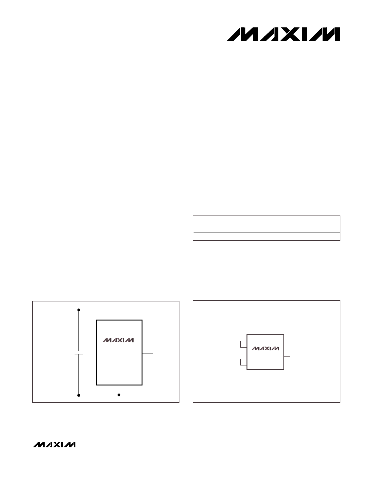
__________________Pin Configuration
______________Ordering Information
V
IN
GND
V+
2.4V to 11V
0V
0.1µF
V
OUT
V
OUT
1.2V
MAX6520
__________Typical Operating Circuit
19-1130; Rev 1; 7/05
*Contact factory for availability.
PART
TEMP RANGE
PIN-
TOP
MARK
MAX6520EUR-T
EFAA
________________________________________________________________ Maxim Integrated Products 1
For pricing, delivery, and ordering information, please contact Maxim/Dallas Direct! at
1-888-629-4642, or visit Maxim’s website at www.maxim-ic.com.
PACKAGE
-40°C to +85°C3 SOT23-3
Page 2
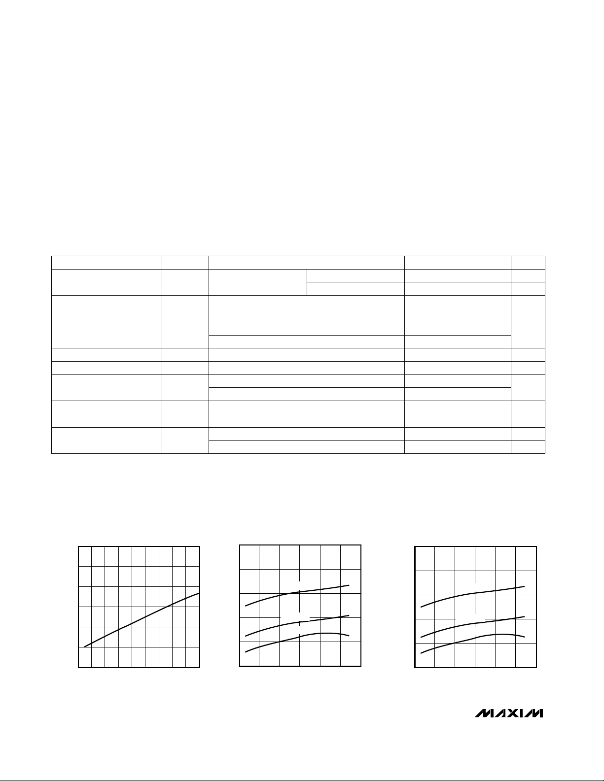
80
50
2
SUPPLY CURRENT
vs. INPUT VOLTAGE
MAX6520 TOC-01
INPUT VOLTAGE (V)
SUPPLY CURRENT (µA)
8
60
46
70
103957 11
75
50
-50
SUPPLY CURRENT
vs. TEMPERATURE
MAX6520 TOC-02
TEMPERATURE (°C)
SUPPLY CURRENT (µA)
100
60
55
65
050
70
-25 25 75
VIN = 9V
VIN = 5V
VIN = 3V
75
50
-50
SUPPLY CURRENT
vs. TEMPERATURE
MAX6520 TOC-02
TEMPERATURE (°C)
SUPPLY CURRENT (µA)
100
60
55
65
050
70
-25 25 75
VIN = 9V
VIN = 5V
VIN = 3V
__________________________________________Typical Operating Characteristics
(V
IN
= 3V, I
LOAD
= 0mA, TA = +25°C, unless otherwise noted.)
MAX6520
50ppm/°C, SOT23, 3-Terminal,
1.2V Voltage Reference
2 _______________________________________________________________________________________
ABSOLUTE MAXIMUM RATINGS
DC ELECTRICAL CHARACTERISTICS
(VIN= 2.4V, I
LOAD
= 0mA, TA= +25°C, unless otherwise noted.)
Stresses beyond those listed under “Absolute Maximum Ratings” may cause permanent damage to the device. These are stress ratings only, and functional
operation of the device at these or any other conditions beyond those indicated in the operational sections of the specifications is not implied. Exposure to
absolute maximum rating conditions for extended periods may affect device reliability.
Supply Voltage (VIN) ..............................................-0.3V to +12V
V
OUT
............................................................-0.3V to (VIN+ 0.3V)
Output Short-Circuit Duration ..........Continuous to Either Supply
Continuous Power Dissipation (T
A
= +70°C)
SOT23 (derate 4mW/°C above +70°C) ...........................320mW
Operating Temperature Range ...........................-40°C to +85°C
Storage Temperature Range .............................-65°C to +160°C
Lead Temperature (soldering, 10s) .................................+300°C
e
n
PARAMETER SYMBOL MIN TYP MAX UNITS
10
400
1.188 1.200 1.212 V
230Line Regulation V
OUT/VIN
µV/V
4.3
Short-Circuit Output Current I
SC
400
mA
CONDITIONS
VIN= 2.4V to 11V, TA= T
MIN
to T
MAX
(Note 1)
0.1Hz to 10Hz
10Hz to 10kHz
V
OUT
shorted to GND
V
OUT
shorted to V
IN
I
Q
50 58
Quiescent Supply Current
70
µA
TA= +25°C
TA= T
MIN
to T
MAX
(Note 1)
1.5 5
Change in Supply Current
vs. Input Voltage
IQ/V
IN
µA/VVIN= 2.4V to 11V
TA= +25°C
µA
Note 1: Production testing done at TA= +25°C, over temperature limits guaranteed by parametric correlation data.
Output Voltage Noise µVp-p
Load Regulation V
OUT/IOUTILOAD
= -50µA to 400µA (Note 1) 0.1 1 µV/µA
Output Voltage V
OUT
1.176 1.224 VTA= T
MIN
to T
MAX
MAX6520EUR
Output Voltage Temperature
Coefficient
TCV
OUT
25 50 ppm/°CMAX6520EUR, TA= T
MIN
to T
MAX
Page 3

MAX6520
50ppm/°C, SOT23, 3-Terminal,
1.2V Voltage Reference
_______________________________________________________________________________________ 3
0
-50
LOAD REGULATION
vs. TEMPERATURE
MAX6520 TOC-03
TEMPERATURE (°C)
LOAD REGULATION (µV/µA)
100
0.16
0.08
0.24
050
0.32
-25 25 75
120
100
40
0.0001 0.001 0.1 .01 .10
POWER-SUPPLY REJECTION RATIO
vs. FREQUENCY
60
80
MAX6520 TOC-06
FREQUENCY (kHz)
PSRR (dB)
0.01
1.2001
1.2000
1.1997
110 1000
OUTPUT VOLTAGE
vs. SOURCE CURRENT
1.1998
1.1999
MAX6520 TOC-05
SOURCE CURRENT (µA)
OUTPUT VOLTAGE (V)
100
____________________________Typical Operating Characteristics (continued)
(V
IN
= 3V, I
LOAD
= 0mA, TA = +25°C, unless otherwise noted.)
0.1Hz TO 100Hz NOISE
50µV/div
1µs/div
A = OUTPUT CURRENT, 50µA/div, I
LOAD
= 0µA TO -50µA
B = OUTPUT VOLTAGE, 100mV/div
LOAD-TRANSIENT RESPONSE
B
A
10µs/div
A = OUTPUT CURRENT, 500µA/div, I
LOAD
= 0µA TO 500µA
B = OUTPUT VOLTAGE, 100mV/div
LOAD-TRANSIENT RESPONSE
B
A
10µs/div
A = INPUT VOLTAGE, 100mV/div, VIN = 3V ± 50mV
B = OUTPUT VOLTAGE, 10mV/div
LINE-TRANSIENT RESPONSE
B
A
OUT
IN
5µs/div
Page 4

MAX6520
50ppm/°C, SOT23, 3-Terminal,
1.2V Voltage Reference
4 _______________________________________________________________________________________
__________Applications Information
Input Bypassing
For the best line-transient performance, decouple the
input with a 0.1µF ceramic capacitor as shown in the
Typical Operating Circuit. Locate the capacitor as
close to the device pin as possible. Where transient
performance is less important, no capacitor is necessary.
Output Bypass
The MAX6520 performs well without an output decoupling capacitor. If your application requires an output
charge reservoir (e.g., to decouple the reference from
the input of a DAC), then make sure that the total output
capacitive load does not exceed 10nF.
DAC
LATCH A
DAC A
DAC
LATCH B
DAC B
DAC
LATCH C
LATCH
DAC C
SCLK
OUTA
OUTB
OUTC
LOUT
DIN
+3V
0.1µF
V
IN
V
OUT
CS REFAB
REFC
RESET
V
DDVSS GND
16-BIT SHIFT REGISTER
CONTROL (8) DATA (8)
MAX512
MAX513
MAX6520
1
2
1
2
3
4
567
8
9
10
1112
14
3
0.01µF
Figure 1. 3V, Triple, 8-Bit Serial DAC
Figure 2. Low-Power ±1.2V Reference
+3V
-3V
V
IN
V
OUT
MAX6520
2
1
3
3
4
6
-1.2V
RR
+1.2V
2
7
MAX406A
_____________________Pin Description
GroundGND3
Reference OutputV
OUT
2
Input VoltageV
IN
1
FUNCTIONNAMEPIN
___________________Chip Information
TRANSISTOR COUNT: 39
Page 5

MAX6520
50ppm/°C, SOT23, 3-Terminal,
1.2V Voltage Reference
_______________________________________________________________________________________ 5
__________________________________________________Tape-and-Reel Information
4.0±0.1
4.0±0.1
2.0±0.05
1.75±0.1
ø1.5±0.1
ø1.1±0.1
8.0±0.2
3.5±0.05
NOTE: DIMENSIONS ARE IN MM.
AND FOLLOW EIA481-1 STANDARD.
Page 6

Maxim cannot assume responsibility for use of any circuitry other than circuitry entirely embodied in a Maxim product. No circuit patent licenses are
implied. Maxim reserves the right to change the circuitry and specifications without notice at any time.
6 ___________________Maxim Integrated Products, 120 San Gabriel Drive, Sunnyvale, CA 94086 (408) 737-7600
© 2005 Maxim Integrated Products Printed USA is a registered trademark of Maxim Integrated Products, Inc.
MAX6520
50ppm/°C, SOT23, 3-Terminal,
1.2V Voltage Reference
SOT23 L.EPS
F
1
1
21-0051
PACKAGE OUTLINE, 3L SOT-23
Package Information
(The package drawing(s) in this data sheet may not reflect the most current specifications. For the latest package outline information
go to www.maxim-ic.com/packages
.)
 Loading...