

Page 1
_______________General Description
The MAX629 low-power DC-DC converter features an
internal N-channel MOSFET switch and programmable
current limiting. It is designed to supply positive or negative bias voltages up to ±28V from input voltages in
the 0.8V to V
OUT
range, and can be configured for
boost, flyback, and SEPIC topologies.
The MAX629’s current-limited pulse-frequency-modula-
tion (PFM) control scheme provides high efficiency over
a wide range of load conditions. An internal, 0.5A Nchannel MOSFET switch reduces the total part count,
and a high switching frequency (up to 300kHz) allows
for tiny surface-mount magnetics.
The MAX629’s combination of low supply current, logiccontrolled shutdown, small package, and tiny external
components makes it an extremely compact and efficient high-voltage biasing solution that’s ideal for battery-powered applications. The MAX629 is available in
an 8-pin SO package.
________________________Applications
Positive or Negative LCD Bias Generators
High-Efficiency DC-DC Boost Converters
Varactor Tuning Diode Bias
Palmtop Computers
2-Cell and 3-Cell Battery-Powered Applications
____________________________Features
♦ Internal, 500mA, 28V N-Channel Switch
(No External FET Required)
♦ Generates Positive or Negative Output Voltages
♦ 80µA Supply Current
♦ 1µA Max Shutdown Current
♦ Up to 300kHz Switching Frequency
♦ Adjustable Current Limit Allows Use of Small,
Inexpensive Inductors
♦ 8-Pin SO Package
MAX629
28V, Low-Power, High-Voltage,
Boost or Inverting DC-DC Converter
________________________________________________________________
Maxim Integrated Products
1
MAX629
SHDN
V
IN
+2.7V
TO +5.5V
LX
V
CC
GND
FB
ISET
POL
REF
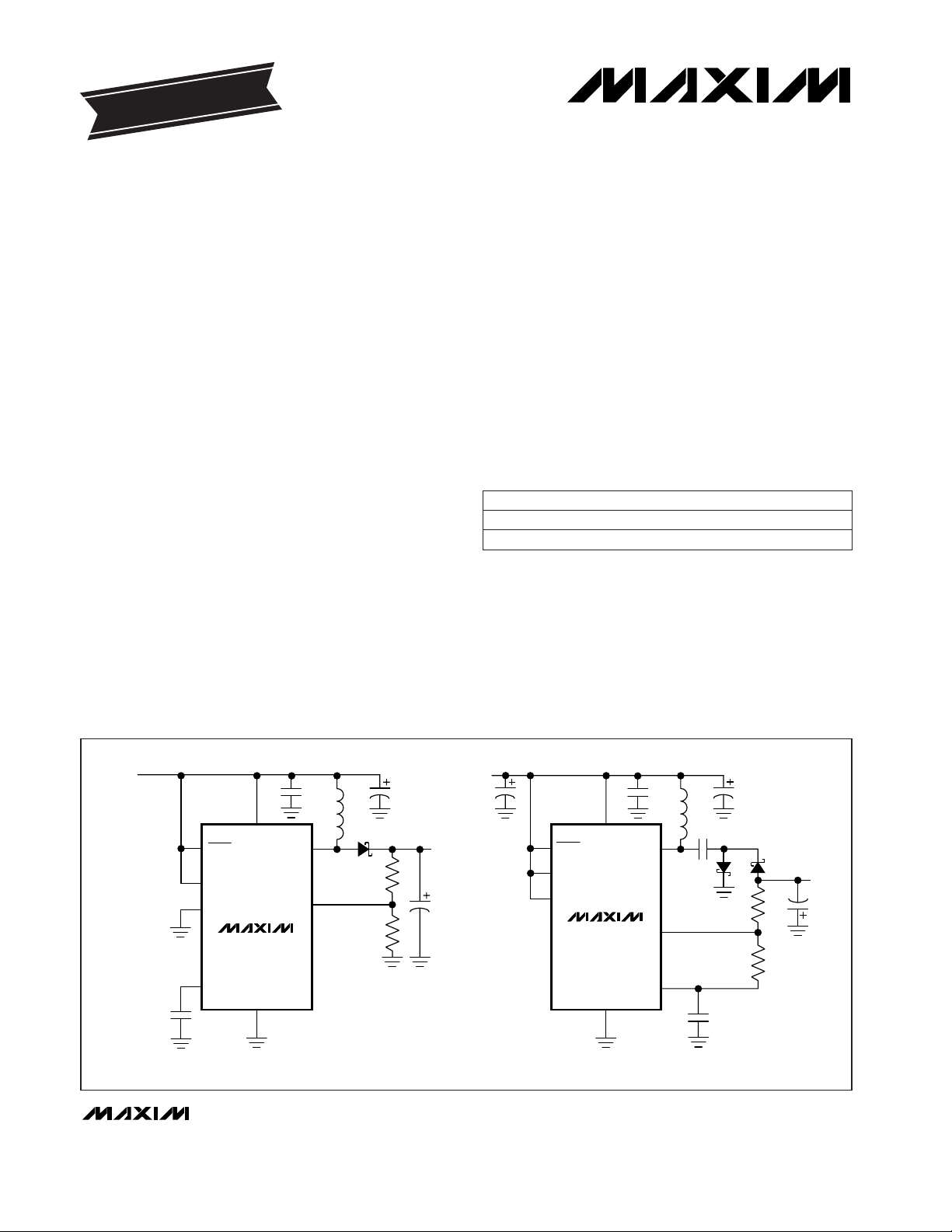
POSITIVE OUTPUT VOLTAGE
MAX629
SHDN
-V
OUT
-28V
V
OUT
28V
V
IN
+2.7V
TO +5.5V
LX
V
CC
GND
FB
REF
POL
NEGATIVE OUTPUT VOLTAGE
ISET
___________________________________________________Typical Operating Circuit
19-1219; Rev 1; 6/97
PART TEMP. RANGE PIN-PACKAGE
______________Ordering Information
For free samples & the latest literature: http://www.maxim-ic.com, or phone 1-800-998-8800
Note: To order tape-and-reel shipping, add “-T” to the end of
the part number.
*
Dice are tested at TA= +25°C, DC parameters only.
Pin Configuration appears at end of data sheet.
MAX629C/D 0°C to +70°C Dice*
MAX629ESA -40°C to +85°C 8 SO
EVALUATION KIT MANUAL
AVAILABLE
Page 2
MAX629
28V, Low-Power, High-Voltage,
Boost or Inverting DC-DC Converter
2 _______________________________________________________________________________________
ABSOLUTE MAXIMUM RATINGS
ELECTRICAL CHARACTERISTICS
(VCC= +5V, C
REF
= 0.1µF, TA= -40°C to +85°C, unless otherwise noted. Typical values are at TA= +25°C.) (Note1)
Stresses beyond those listed under “Absolute Maximum Ratings” may cause permanent damage to the device. These are stress ratings only, and functional
operation of the device at these or any other conditions beyond those indicated in the operational sections of the specifications is not implied. Exposure to
absolute maximum rating conditions for extended periods may affect device reliability.
Supply Voltage (VCCto GND)..................................-0.3V to +6V
SHDN to GND...........................................................-0.3V to +6V
ISET, REF, FB, POL to GND.......................-0.3V to (V
CC
+ 0.3V)
LX to GND ..............................................................-0.3V to +30V
Continuous Power Dissipation (T
A
= +70°C)
SO (derate 5.88mW/°C above +70°C)..........................471mW
Operating Temperature Range ...........................-40°C to +85°C
Junction Temperature......................................................+150°C
Storage Temperature Range.............................-65°C to +165°C
Lead Temperature (soldering, 10sec).............................+300°C
CONDITIONS
V2.7 5.5VCCInput Voltage (Note 2)
UNITSMIN TYP MAXPARAMETER
VFB= 1.3V µA80 120VCCSupply Current
100mV hysteresis V2.3 2.5 2.65VCCUndervoltage Lockout
SHDN = GND
µA0.04 1VCCShutdown Current
A
0.39 0.45 0.51
Circuit of Figure 2
VLX= 28V, TA= +85°C µA0.05 2.5LX Leakage Current
POL = GND
µs
0.7 1.0 1.3
Minimum LX Off-Time
µs6.5 8.5 10.0Maximum LX On-Time
0.20 0.25 0.33
LX Switch-Current Limit
V28Positive Output Voltage
POL = GND, VFB< 1V 3.0 4.5 6.0
POL = V
CC
2.0 3.2 3.8
POL = GND
(positive output)
V
1.218 1.282
1.225 1.250 1.275
nA5 50FB Input Bias Current
1.225 1.250 1.275
VCC= 5V
Ω
0.6 1.2
VCC= 3.3V 0.7 1.4
LX On-Resistance
TA= 0°C to +85°C
TA= -40°C to +85°C
TA= 0°C to +85°C
TA= -40°C to +85°C
POL = V
CC
(negative output)
mV
-25 25
FB Set Point
-15 0 15
VCC= 2.7V to 5.5V,
no load on REF
V
1.218 1.282
REF Output Voltage
TA= 0°C to +85°C
TA= -40°C to +85°C
V
IH
V
2.4
SHDN, POL, ISET Logic Levels
V
IL
0.4
Voltage applied to L1 (VIN) V
0.8
V
OUT
Input Supply Voltage (Note 2)
Circuit of Figure 3 V
-V
IN
-28
Negative Output Voltage
ISET = V
CC
ISET = GND
POL = V
CC, VFB
> 0.25V 3.0 4.5 6.0
Page 3
MAX629
28V, Low-Power, High-Voltage,
Boost or Inverting DC-DC Converter
_______________________________________________________________________________________ 3
ELECTRICAL CHARACTERISTICS (continued)
(VCC= +5V, C
REF
= 0.1µF, TA= -40°C to +85°C, unless otherwise noted. Typical values are at TA= +25°C.) (Note 1)
Note 1: Specifications to -40°C are guaranteed by design and not production tested.
Note 2: The IC itself requires a supply voltage between +2.7V and +5.5V; however, the voltage that supplies power to the inductor
can vary from 0.8V to 28V, depending on circuit operating conditions.
Note 3: For reference currents less than 10µA, a 0.1µF reference-bypass capacitor is adequate.
Circuit of Figure 2, V
OUT
= 24V, VCC= 3V to 5.5V,
I
LOAD
= 5mA
%/V0.2Line Regulation
Die temperature °C150
I
REF
= 0µA to 100µA, C
REF
= 0.47µF (Note 3)
Thermal Shutdown Threshold
Circuit of Figure 2, V
OUT
= 24V, VCC= 5V,
I
LOAD
= 0mA to 5mA
%0.15Load Regulation
CONDITIONS
mV10 25REF Load Regulation
UNITSMIN TYP MAXPARAMETER
__________________________________________Typical Operating Characteristics
(SHDN = VCC, C
REF
= 0.1µF, TA= +25°C, unless otherwise noted.)
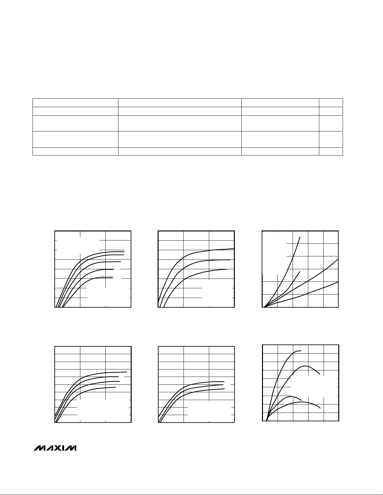
100
60
0.1 100
EFFICIENCY vs. LOAD CURRENT
(V
OUT
= +24V)
65
70
95
90
85
MAX629-01
LOAD CURRENT (mA)
EFFICIENCY (%)
1 10
80
75
D
D: VIN = 5V, ISET = GND
E: V
IN
= 3V, ISET = V
CC
F: VIN = 3V, ISET = GND
V
OUT
= 24V
A: V
IN
= 12V, ISET = V
CC
B: VIN = 12V, ISET = GND
C: V
IN
= 5V, ISET = V
CC
E, F
C
B
A
100
60
0.1 100
EFFICIENCY vs. LOAD CURRENT
(V
OUT
= +12V)
70
65
95
85
90
MAX629-02
LOAD CURRENT (mA)
EFFICIENCY (%)
1 10
80
75
C
B
A
V
OUT
= 12V,
ISET = V
CC
or GND
A: V
IN
= 9V
B: V
IN
= 5V
C: V
IN
= 3V
300
0
0 20
MAXIMUM LOAD CURRENT vs.
INPUT VOLTAGE (V
OUT
= +24V, +12V)
50
250
200
MAX629-03
INPUT VOLTAGE (V)
MAXIMUM LOAD CURRENT (mA)
8 124 16
150
100
A
B
C
D
A: V
OUT
= 12V,
ISET = V
CC
B: V
OUT
= 12V,
ISET = GND
C: V
OUT
=24V,
ISET = V
CC
D: V
OUT
= 24V,
ISET = GND
100
50
0.1 100
EFFICIENCY vs. LOAD CURRENT
(V
OUT
= -18V)
65
60
55
95
80
85
90
MAX629-04
LOAD CURRENT (mA)
EFFICIENCY (%)
1 10
75
70
C
A
A: VIN = 12V, ISET = V
CC
B: VIN = 12V, ISET = GND
C: V
IN
= 5V, ISET = VCC or GND
D: V
IN
= 3V, ISET = VCC or GND
B
D
100
50
0.1 100
EFFICIENCY vs. LOAD CURRENT
(V
OUT
= -12V)
65
60
55
95
80
85
90
MAX629-05
LOAD CURRENT (mA)
EFFICIENCY (%)
1 10
75
70
A
A = VIN = 5V, ISET = V
CC
B = VIN = 5V, ISET = GND
C = V
IN
= 3V, ISET = VCC
D = V
IN
= 3V, ISET = GND
D
B, C
90
0
0 20
MAXIMUM LOAD CURRENT vs. INPUT VOLTAGE
(V
OUT
= -18V, -12V)
30
20
10
80
60
70
MAX629-06
INPUT VOLTAGE (V)
MAXIMUM LOAD CURRENT (mA)
4 8 12 16
50
40
C
A
A: V
OUT
= -12V, ISET = V
CC
B: V
OUT
= -18V, ISET = V
CC
C: V
OUT
= -12V, ISET = GND
D: V
OUT
= -18V, ISET = GND
D
B
Page 4
MAX629
28V, Low-Power, High-Voltage,
Boost or Inverting DC-DC Converter
4 _______________________________________________________________________________________
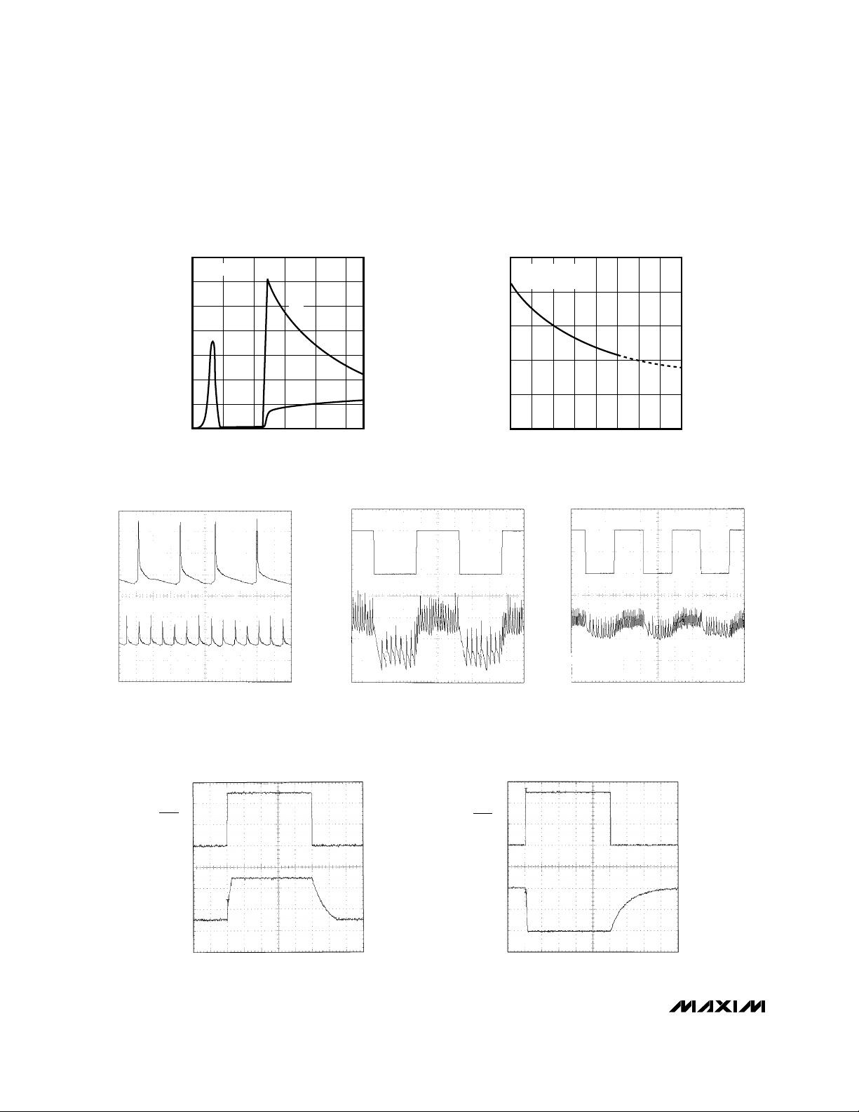
700
600
0
0 1
SUPPLY CURRENT
vs. INPUT VOLTAGE
500
400
300
100
MAX629-07
INPUT VOLTAGE (V)
SUPPLY CURRENT (µA)
2 3 4 5
200
VIN = V
CC
I
CC
I
IN
I
IN
1.255
1.250
1.230
0 20 40
REFERENCE VOLTAGE
vs. REFERENCE LOAD CURRENT
1.245
1.240
MAX629-08
REFERENCE LOAD CURRENT (µA)
REFERENCE VOLTAGE (V)
60 80 100 120 140 160
1.235
VIN = V
CC
= 5V
C4 = 0.47µF
OUTPUT VOLTAGE RIPPLE
MAX629-09
V
OUT
= +24V, I
LOAD
= 5mA
A: ISET = V
CC
, 20mV/div
B: ISET = GND, 20mV/div
A
B
10µs/div
SHUTDOWN TRANSIENT
(POSITIVE CONFIGURATION)
MAX629-12
VCC = VIN = 5V, RL = 4kΩ
50ms/div
5V
SHDN
0V
24V
V
OUT
0V
LOAD-TRANSIENT RESPONSE
(I
SET
= VCC, I
LIM
= 500mA)
MAX629-10
V
OUT
= +24V, ISET = V
CC
A: LOAD CURRENT, 0mA TO 5mA, 2.5mA/div
B: V
OUT,
AC-COUPLED, 10mV/div
A
5mA
0mA
B
200µs/div
LOAD-TRANSIENT RESPONSE
(I
SET
= GND, I
LIM
= 250mA)
MAX629-11
V
OUT
= +24V, ISET = GND
A: LOAD CURRENT, 0mA TO 5mA, 2.5mA/div
B: V
OUT,
AC-COUPLED, 10mV/div
A
0mA
5mA
B
100µs/div
SHUTDOWN TRANSIENT
(NEGATIVE CONFIGURATION)
MAX629-13
START-UP DELAY, VCC = VIN = 5V, I
LOAD
= 5mA
20ms/div
VCC = VIN = 5V, RL = 4kΩ
50ms/div
5V
0V
0V
V
OUT
-20V
SHDN
____________________________Typical Operating Characteristics (continued)
(SHDN = VCC, C
REF
= 0.1µF, TA= +25°C, unless otherwise noted.)
Page 5

MAX629
28V, Low-Power, High-Voltage,
Boost or Inverting DC-DC Converter
_______________________________________________________________________________________ 5
______________________________________________________________Pin Description
Current-Limit Set Input. Connect to VCCfor a 500mA LX current limit, or connect to GND for a 250mA LX
current limit. See
Setting the Current Limit.
ISET5
GroundGND6
Feedback Input for setting output voltage. Connect to an external voltage divider. See
Setting the Output
Voltage.
FB4
1.25V Reference Output. Bypass to GND with a 0.1µF capacitor for I
REF
≤ 10µA. REF can source 100µA to
drive external loads. For 10µA ≤ I
REF
≤ 100µA, bypass REF with a 0.47µF capacitor.
REF3
PIN
Polarity Input. Changes polarity and threshold of FB to allow regulation of either positive or negative output
voltages. Set POL = GND for positive output voltage, or set POL = VCCfor negative output voltage.
POL2
Active-Low Shutdown Input. A logic low puts the MAX629 in shutdown mode and reduces supply current to
1µA.
SHDN
1
FUNCTIONNAME
Internal N-Channel DMOS Switch DrainLX7
Power-Supply InputV
CC
8
_______________Detailed Description
The MAX629 low-power, boost DC-DC converter provides either positive or negative output voltages up to
± 28V from a wide range of input voltages. It is
designed primarily for use in low-power, high-voltage
applications such as LCD biasing and set-top box varactor tuning. The MAX629’s unique control scheme
provides high efficiency and a wide range of output
voltages with only 80µA quiescent supply current, making it ideal for battery-powered applications. The internal N-channel DMOS switch has a pin-programmable
current limit (250mA and 500mA), allowing optimization
of output current and component size. Figure 1 shows
the MAX629 functional diagram.
Control Scheme
A combination of peak-current limiting and a pair of
one-shots controls the MAX629 switching, determining
the maximum on-time and constant off-time. During the
on-cycle, the internal switch closes, and current
through the inductor ramps up until either the fixed
10µs maximum on-time expires (at low input voltages)
or the switch’s peak current limit is reached. The peak
switch current limit is selectable to either 500mA (ISET
= VCC) or 250mA (ISET = GND) (see
Setting the
Current Limit
). After the on-cycle terminates, the switch
turns off, charging the output capacitor through the
diode. In normal operation, the minimum off-time is set
to 1µs for positive output voltages and 3.5µs for negative output voltages. When the output is well below reg-
ulation, however, the off-time is increased to 5µs to provide soft-start during start-up. The switching frequency,
which depends upon the load, can be as high as
300kHz.
Shutdown Mode
When SHDN is low, the MAX629 enters shutdown
mode. In this mode, the feedback and control circuit,
reference, and internal biasing circuitry turn off. The
shutdown current drops to less than 1µA. SHDN is a
logic-level input; connect it to VCCfor normal operation.
The output voltage behavior in shutdown mode
depends on the output voltage polarity. In the positive
output voltage configuration (Figure 2), the output is
directly connected to the input through the diode (D1)
and the inductor (L1). When the device is in shutdown
mode, the output voltage falls to one diode drop below
the input voltage, and any load connected to the output
may still conduct current. In the negative output voltage
configuration (Figure 3), there is no DC connection
between the input and the output, and in shutdown
mode the output is pulled to GND.
__________________Design Procedure
Setting the Output Voltage
For either positive or negative output voltage applications, set the MAX629’s output voltage using two external resistors, R1 and R2, as shown in Figures 2 and 3.
Since the input bias current at FB has a 50nA maximum
value, large resistors can be used in the feedback loop
Page 6

MAX629
28V, Low-Power, High-Voltage,
Boost or Inverting DC-DC Converter
6 _______________________________________________________________________________________
without a significant loss of accuracy. Begin by selecting R2 to be in the 10kΩ to 200kΩ range, and calculate
R1 using the applicable equation from the following
subsections.
Positive Output Voltages
For positive output voltages, use the typical boost configuration shown in Figure 2, connecting POL to GND.
This sets the threshold voltage at FB to equal V
REF
.
Choose the value of R2 and calculate R1 as follows:
where V
REF
= 1.25V.
Negative Output Voltages
For negative output voltages, configure R1 and R2 as
shown in Figure 3, connecting POL to VCC. This sets
the FB threshold voltage to GND so that negative voltages can be regulated. Choose R2 and calculate R1 as
follows:
where V
REF
= 1.25V.
Figure 3 demonstrates generation of a negative output
voltage by following the MAX629 with an inverting
charge pump. This configuration limits V
OUT
to values
between -V
IN
and -28V. If smaller negative output volt-
ages are required, D2’s cathode can be connected to
VIN. This alternative configuration permits output voltages smaller than -V
IN
, but cannot be used for output
voltages more negative than -28V - V
IN
. It produces
roughly one-half the output current as the standard configuration and is typically 5% less efficient.
R1 = R2 x
V
V
| |
OUT
REF
R1 = R2 x
V
V
OUT
REF
−
1
MAX629
MIN OFF-TIME
GENERATOR
TRIG
Q
S
LX
ISET
Q
F/F
GND
R
START-UP
MAX ON-TIME
GENERATOR
(10µs)
CONTROL
FB
REF
V
CC
1V
START-UP
COMPARATOR
ERROR
AMP
1.25V
REF
POL
TRIG
Q
SHDN
POLARITY
Figure 1. Functional Diagram
Page 7

MAX629
28V, Low-Power, High-Voltage,
Boost or Inverting DC-DC Converter
_______________________________________________________________________________________ 7
Setting the Current Limit
External current-limit selection provides added control
over the MAX629’s output performance. A higher current limit increases the amount of energy stored in the
inductor during each cycle, which provides a higher
output current capability. For higher output current
applications, choose the 500mA current-limit option by
connecting ISET to VCC. When lower output current is
required, the 250mA current limit can provide several
advantages. First, a smaller inductor can be used,
which saves board area and cost. Second, the smaller
energy transfer per cycle reduces output ripple for a
given capacitor, providing design flexibility between
board area, cost, and output ripple by allowing cheaper, higher-ESR capacitors. Connect ISET to GND to
select the 250mA current-limit option.
Inductor Selection
The MAX629’s high switching frequency allows for the
use of a small inductor. The 47µH inductor shown in the
Typical Operating Circuit
is recommended for most
applications. Larger inductances reduce the peak
inductor current, but may limit output current capability
at low input voltages and provide slower start-up times.
Smaller inductances require less board space, but may
cause greater peak current due to current-sense comparator propagation delay. If input voltages below 2V
will be common, reducing the inductance to 22µH
might improve performance; however, maximum load
current and efficiency may decline. It is important to
thoroughly test operation under all input and output
conditions to ensure proper component selection.
Inductors with a ferrite core or equivalent are recommended; powder iron cores are not recommended for
use with high switching frequencies. The inductor’s
incremental saturation rating must exceed the selected
current limit. For highest efficiency, use an inductor with
a low DC resistance (under 100mΩ). See Table 1 for a
list of inductor suppliers.
Figure 3. -20V for a Negative LCD Bias
* FOR SINGLE-SUPPLY OPERATION
MAX629
SHDN
C1
10µF
35V
C3
0.1µF
L1
47µH
R1
576k
1%
R2
35.7k
1%
D1
D1 = D2 = MBR0540L
D2
R3
2Ω
C5
2.2µF
C2
10µF
35V
CF
150pF
C4
0.1µF
V
CC
+2.7V
TO +5.5V
V
IN
+0.8V
TO +15V
V
OUT
-20V
LX
V
CC
GND
FB
REF
POL
ISET
*
Figure 2. +24V for a Positive LCD Bias
MAX629
SHDN
V
OUT
+24V
V
CC
+2.7V
TO +5.5V
V
IN
+0.8V
TO +24V
* FOR SINGLE-SUPPLY OPERATION
*
C3
0.1µF
C4
0.1µF
C1
10µF
35V
C2
10µF
35V
C
F
150pF
R1
576k
1%
R2
31.6k
1%
L1
47µH
D1
MBR0540L
LX
V
CC
GND
FB
ISET
REF
POL
*FOR SINGLE-SUPPLY OPERATION *FOR SINGLE-SUPPLY OPERATION
Page 8

MAX629
28V, Low-Power, High-Voltage,
Boost or Inverting DC-DC Converter
8 _______________________________________________________________________________________
Diode Selection
The MAX629’s high switching frequency demands a
high-speed rectifier. Schottky diodes, such as the
1N5819 or MBR0530L, are recommended. Make sure
that the diode’s peak current rating exceeds the peak
current set by ISET, and that its breakdown voltage
exceeds the output voltage. Schottky diodes are preferred due to their low forward voltage. However, ultrahigh-speed silicon rectifiers are also acceptable. Table
1 lists Schottky diode suppliers.
Capacitor Selection
Output Filter Capacitor
The primary criterion for selecting the output filter
capacitor is low effective series resistance (ESR). The
product of the peak inductor current and the output filter capacitor’s ESR determines the amplitude of the
high-frequency ripple seen on the output voltage.
These requirements can be balanced by appropriate
selection of the current limit, as discussed in the S
etting
the Current Limit
section. Table 1 lists some low-ESR
capacitor suppliers. See the Output Voltage Ripple
graph in the
Typical Operating Characteristics
section.
Input Bypass Capacitor
Although the output current of many MAX629 applications may be relatively small, the input must be
designed to withstand current transients equal to the
inductor current limit. The input bypass capacitor
reduces the peak currents drawn from the voltage
source, and reduces noise caused by the MAX629’s
switching action. The input source impedance determines the size of the capacitor required at the input
(V
IN
). As with the output filter capacitor, a low-ESR
capacitor is recommended. A 10µF, low-ESR capacitor
is adequate for most applications, although smaller
bypass capacitors may also be acceptable. Bypass the
IC separately with a 0.1µF ceramic capacitor placed as
close as possible to the VCCand GND pins.
Reference Capacitor
Bypass REF to GND with a 0.1µF ceramic capacitor for
REF currents up to 10µA. REF can source up to 100µA
of current for external loads. For 10µA ≤ I
REF
≤ 100µA,
bypass REF with a 0.47µF capacitor.
Feed-Forward Capacitor
Parallel a capacitor (CF) across R1 to compensate the
feedback loop and ensure stability (Figures 2 and 3).
Values up to 270pF are recommended for most applications. Choose the lowest capacitor value that
ensures stability; high capacitance values may
degrade line regulation.
__________Applications Information
Adjusting the Output Voltage
Many biasing applications require an adjustable output
voltage, which is easily obtained using the configuration in Figure 4. In this circuit, an external bias voltage
(which may be generated by a potentiometer, a DAC,
or other means) is coupled to FB through the resistor
RB. The output voltage of this circuit is given by:
where V
INIT
is the fixed output voltage as calculated in
the section
Setting the Output Voltage
, and VFBis equal
to either V
REF
(1.25V) for the positive configuration or
0V for the negative configuration. Proper choice of R
B
provides a wide range of available output voltages
using simple external components to generate V
BIAS
.
Input Voltage Range
Although, in many cases, the MAX629 and the inductor
are powered from the same source, it is often advantageous in battery-powered applications to power the
device from an available regulated supply and to
power the inductor directly from a battery. The MAX629
requires a +2.7V to +5.5V supply at VCC, but the inductor can be powered from as low as +0.8V, significantly
V V
R1
R
(V V )
OUT INIT
B
FB BIAS
= + −
Table 1. Component Suppliers
Coilcraft: DO1608 and
DT1608 series
(847) 639-6400
Sumida: CD43, CD54,
and CDRH62B series
(847) 956-0666
TDK: NLC565050 series (847) 390-4373 (847) 390-4428
(847) 956-0702
Murata-Erie: LQH4 series (814) 237-1431 (814) 238-0490
(847) 639-1469
Nihon: EC11 FS1 series (805) 867-2555 (805) 867-2698
Motorola: MBR0530L (602) 303-5454 (602) 994-6430
Matsuo: 267 series (714) 969-2491
Sprague: 595D series (603) 224-1961 (603) 224-1430
(714) 960-6492
AVX: TPS series (803) 946-0690 (803) 626-3123
PHONESUPPLIER FAX
CAPACITORS
DIODES
INDUCTORS
Page 9

MAX629
28V, Low-Power, High-Voltage,
Boost or Inverting DC-DC Converter
_______________________________________________________________________________________ 9
increasing usable battery life. Using separate supplies
for VCCand VINalso reduces noise injection onto V
CC
by isolating it from the switching transients, allowing a
smaller, less-expensive input filter capacitor to be used
in many applications. If input voltages below 2V will be
common, reducing the inductor to 22µH may improve
performance in this voltage range, at the potential cost
of some decrease in maximum load current and efficiency.
In the negative configuration shown in Figure 3, the
inverting charge pump injects current into LX with each
cycle. The amount of charge injected increases at
higher VIN, and may prematurely trip the internal current-
limit threshold. Resistor R3 increases the usable input
voltage range by limiting the peak injected current. The
2Ω resistor shown provides a usable input voltage
range beyond VIN= 15V. In applications with a different
input voltage range, R3 may be increased or
decreased as necessary, with a resulting efficiency
change of roughly 0.5%/Ω.
Layout Considerations
Proper PC board layout is essential due to high current
levels and fast switching waveforms that radiate noise.
It is recommended that initial prototyping be performed
using the MAX629 evaluation kit or equivalent PC
board-based design. Breadboards or proto-boards
should never be used when prototyping switching regulators.
It is important to connect the GND pin, the input
bypass-capacitor ground lead, and the output filtercapacitor ground lead to a single point (star ground
configuration) to minimize ground noise and improve
regulation. Also, minimize lead lengths to reduce stray
capacitance, trace resistance, and radiated noise, with
preference given to the feedback circuit, the ground
circuit, and LX. Place R1 and R2 as close to the feedback pin as possible. Place the input bypass capacitor
as close as possible to VCCand GND.
Refer to the MAX629 evaluation kit data sheet for an
example of proper board layout.
Figure 4. Adjustable Output Voltage
MAX629
V
OUT
V
BIAS
R2
( ) ARE FOR NEGATIVE OUTPUT VOLTAGE CONFIGURATIONS.
R
B
R1
FB
GND
(REF)
Page 10

MAX629
28V, Low-Power, High-Voltage,
Boost or Inverting DC-DC Converter
10 ______________________________________________________________________________________
__________________Pin Configuration ___________________Chip Information
TRANSISTOR COUNT: 653
SUBSTRATE CONNECTED TO GND
GND
ISET
FB
1
2
87V
CC
LX
POL
REF
SHDN
SO
TOP VIEW
3
4
6
5
MAX629
Page 11

MAX629
28V, Low-Power, High-Voltage,
Boost or Inverting DC-DC Converter
______________________________________________________________________________________ 11
________________________________________________________Package Information
SOICN.EPS
Page 12

MAX629
28V, Low-Power, High-Voltage,
Boost or Inverting DC-DC Converter
12 ______________________________________________________________________________________
NOTES
 Loading...