

Page 1
General Description
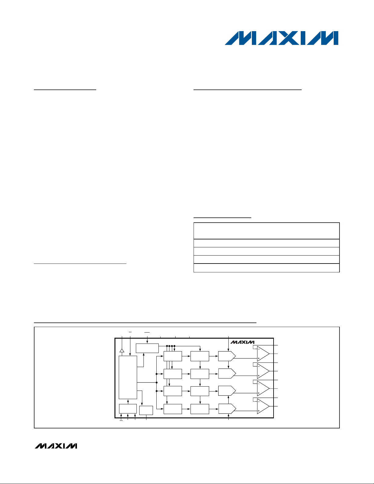
The MAX5500/MAX5501 integrate four low-power, 12-bit
digital-to analog converters (DACs) and four precision
output amplifiers in a small, 20-pin package. Each negative input of the four precision amplifiers is externally
accessible providing flexibility in gain configurations,
remote sensing, and high output drive capacity, making
the MAX5500/MAX5501 ideal for industrial-process-control applications. Other features include software shutdown, hardware shutdown lockout, an active-low reset
which clears all registers and DACs to zero, a user-programmable logic output, and a serial-data output.
Each DAC provides a double-buffered input organized
as an input register followed by a DAC register. A 16-bit
serial word loads data into each input register. The serial interface is compatible with SPI™/QSPI™/
MICROWIRE™. The serial interface allows the input and
DAC registers to be updated independently or simultaneously with a single software command. The 3-wire
interface simultaneously updates the DAC registers. All
logic inputs are TTL/CMOS-logic compatible. The
MAX5500 operates from a single +5V power supply,
and the MAX5501 operates from a single +3V power
supply. The MAX5500/MAX5501 are specified over the
extended -40°C to +105°C temperature range.
Applications
Industrial Process Controls
Automatic Test Equipment
Microprocessor (µP)-Controlled Systems
Motion Control
Digital Offset and Gain Adjustment
Remote Industrial Controls
Features
♦ Four 12-Bit DACs with Configurable Output
Amplifiers
♦ +5V or +3V Single-Supply Operation
♦ Low Supply Current:
0.85mA Normal Operation
10µA Shutdown Mode (MAX5500)
♦ Force-Sense Outputs
♦ Power-On Reset Clears All Registers and DACs
to Zero
♦ Capable of Recalling Last State Prior to Shutdown
♦ SPI/QSPI/MICROWIRE Compatible
♦ Simultaneous or Independent Control of DACs
through 3-Wire Serial Interface
♦ User-Programmable Digital Output
♦ Guaranteed Over Extended Temperature Range
(-40°C to +105°C)
MAX5500/MAX5501
Low-Power, Quad, 12-Bit
Voltage-Output DACs with Serial Interface
________________________________________________________________
Maxim Integrated Products
1
Functional Diagram
19-4368; Rev 0; 11/08
For pricing, delivery, and ordering information, please contact Maxim Direct at 1-888-629-4642,
or visit Maxim’s website at www.maxim-ic.com.
Pin Configuration appears at end of data sheet.
SPI/QSPI are trademarks of Motorola, Inc. MICROWIRE is a trademark of National Semiconductor, Corp.
Ordering Information
PART
PIN-
INL (LSB)
SUPPLY (V)
MAX5500AGAP+ 20 SSOP ±0.75 +5
MAX5500BGAP+ 20 SSOP ±2 +5
MAX5501AGAP+*
20 SSOP ±0.75 +3
MAX5501BGAP+* 20 SSOP ± 2 +3
+
Denotes a lead-free/RoHS-compliant package.
*
Future product—contact factory for availability.
Note: All devices are specified over the -40°C to +105°C operating
temperature range.
PACKAGE
DOUT
CL
16-BIT
SHIFT
REGISTER
SR
CONTROL
DIN
CS
V
DD
DGND
AGND
INPUT
REGISTER A
INPUT
REGISTER B
INPUT
REGISTER C
INPUT
REGISTER D
DAC
REGISTER A
DAC
REGISTER B
DAC
REGISTER C
DAC
REGISTER D
PDL
DECODE
CONTROL
LOGIC
OUTPUT
SCLK
UPO REFCD
REFAB
DAC A
DAC B
DAC C
DAC D
MAX5500
MAX5501
FBA
OUTA
FBB
OUTB
FBC
OUTC
FBD
OUTD
Page 2
MAX5500/MAX5501
Low-Power, Quad, 12-Bit
Voltage-Output DACs with Serial Interface
2 _______________________________________________________________________________________
ABSOLUTE MAXIMUM RATINGS
ELECTRICAL CHARACTERISTICS
(MAX5500 (V
DD
= +5V ±10%, V
REFAB
= V
REFCD
= 2.5V), MAX5501 (VDD= +3V ±10%, V
REFAB
= V
REFCD
= 1.5V), V
AGND
= V
DGND
= 0,
R
L
= 5kΩ, CL = 100pF, TA = T
MIN
to T
MAX
, unless otherwise noted. Typical values at TA = +25°C. Output buffer connected in unity-
gain configuration (Figure 9).)
Stresses beyond those listed under “Absolute Maximum Ratings” may cause permanent damage to the device. These are stress ratings only, and functional
operation of the device at these or any other conditions beyond those indicated in the operational sections of the specifications is not implied. Exposure to
absolute maximum rating conditions for extended periods may affect device reliability.
VDDto AGND............................................................-0.3V to +6V
V
DD
to DGND ...........................................................-0.3V to +6V
AGND to DGND.....................................................-0.3V to +0.3V
REFAB, REFCD to AGND...........................-0.3V to (V
DD
+ 0.3V)
OUT_, FB_ to AGND...................................-0.3V to (V
DD
+ 0.3V)
Digital Inputs to DGND.............................................-0.3V to +6V
DOUT, UPO to DGND ................................-0.3V to (V
DD
+ 0.3V)
Continuous Current into Any Pin.......................................±20mA
Continuous Power Dissipation (T
A
= +70°C)
20-Pin SSOP (derate 8.00mW/°C above +70°C) .........640mW
Operating Temperature Range .........................-40°C to +105°C
Storage Temperature Range .............................-65°C to +150°C
Lead Temperature (soldering, 10s) .................................+300°C
STATIC PERFORMANCE (Analog Section)
Resolution N 12 Bits
Integral Nonlinearity
(Note 1)
Differential Nonlinearity DNL Guaranteed monotonic ±1.0 LSB
Offset Error V
Offset-Error Tempco 6 ppm/ oC
Gain Error GE (Note 1) -0.3 ±2.0 LSB
Gain-Error Tempco 1 ppm/ oC
Power-Supply Rejection Ratio PSRR 100 600 µV/V
MATCHING PERFORMANCE (TA = +25oC)
Gain Error GE -0.3 ±2.0 LSB
Offset Error V
Integral Nonlinearity INL (Note 1) ±0.35 ±1.0 LSB
REFERENCE INPUT
Reference Input Range V
Reference Input Resistance R
Refer ence C ur r ent i n S hutd ow n 0.01 ±1.0 µA
DIGITAL INPUTS
Input High Voltage V
Input Low Voltage V
Input Leakage Current I
Input Capacitance C
PARAMETER SYMBOL CONDITIONS MIN TYP MAX UNITS
INL
REF
REF
MAX5500A/MAX5501A ±0.25 ±0.75
MAX5500B/MAX5501B ±2.0
OS
OS
Code-dependent, minimum at code
555H
MAX5500A/MAX5500B 2.4
IH
MAX5501A/MAX5501B 2.0
IL
VIN = 0 or V
IN
IN
DD
0V
8kΩ
±1.0 ±3.5 mV
±0.1 ±1.0 µA
8pF
±3.5 mV
- 1.4 V
DD
0.8 V
LSB
V
Page 3
MAX5500/MAX5501
Low-Power, Quad, 12-Bit
Voltage-Output DACs with Serial Interface
_______________________________________________________________________________________ 3
ELECTRICAL CHARACTERISTICS (continued)
(MAX5500 (V
DD
= +5V ±10%, V
REFAB
= V
REFCD
= 2.5V), MAX5501 (VDD= +3V ±10%, V
REFAB
= V
REFCD
= 1.5V), V
AGND
= V
DGND
= 0,
R
L
= 5kΩ, CL = 100pF, TA = T
MIN
to T
MAX
, unless otherwise noted. Typical values at TA = +25°C. Output buffer connected in unity-
gain configuration (Figure 9).)
DIGITAL OUTPUTS
Output High Voltage V
Output Low Voltage V
DYNAMIC PERFORMANCE
Voltage Output Slew Rate SR 0.6 V/µs
Output Settling Time
Output Voltage Swing Rail-to-rail (Note 2) 0 to V
Current into FB_ 0 0.1 µA
OUT_ Leakage Current in
Shutdown
Startup Time Exiting Shutdown
Mode
Digital Feedthrough CS =VDD, f
Digital Crosstalk 5nV•s
POWER SUPPLIES
Supply Voltage V
Supply Current I
Supply Current in Shutdown (Note 3) 10 20 µA
PARAMETER SYMBOL CONDITIONS MIN TYP MAX UNITS
OH
OL
DD
DD
I
I
To ±0.5 LSB, V
MAX5500A/MAX5500B
To ±0.5 LSB, V
MAX5501A/MAX5501B
R
MAX5500A/MAX5500B 15
MAX5501A/MAX5501B 20
MAX5500A/MAX5500B 4.5 5.5
MAX5501A/MAX5501B 3.0 3.6
(Note 3) 0.85 1.1 mA
= 2mA VDD - 0.5 V
SOURCE
= 2mA 0.13 0.4 V
SINK
= 2.5V
STEP
= 2.5V
STEP
= ∞ ±0.01 ±1.0 µA
L
= 100kHz 5 nV•s
IN
12
16
DD
µs
V
µs
V
Reference Current in Shutdown (Note 3) 10 20 µA
TIMING CHARACTERISTICS (Figure 6)
SCLK Clock Period t
SCLK Pulse-Width High t
SCLK Pulse-Width Low t
CS Fall to SCLK Rise Setup
Time
SCLK Rise to CS Rise Hold
Time
DIN Setup Time t
DIN Hold Time t
CP
CH
CL
t
CSS
t
CSH
DS
DH
100 ns
40 ns
40 ns
40 ns
0ns
40 ns
0ns
Page 4
MAX5500/MAX5501
Low-Power, Quad, 12-Bit
Voltage-Output DACs with Serial Interface
4 _______________________________________________________________________________________
ELECTRICAL CHARACTERISTICS (continued)
(MAX5500 (V
DD
= +5V ±10%, V
REFAB
= V
REFCD
= 2.5V), MAX5501 (VDD= +3V ±10%, V
REFAB
= V
REFCD
= 1.5V), V
AGND
= V
DGND
= 0,
R
L
= 5kΩ, CL = 100pF, TA = T
MIN
to T
MAX
, unless otherwise noted. Typical values at TA = +25°C. Output buffer connected in unity-
gain configuration (Figure 9).)
Note 1: Guaranteed from code 11 to code 4095 in unity-gain configuration.
Note 2: Accuracy is better than 1.0 LSB for V
OUT
= 6mV to (V
DD
- 60mV), guaranteed by PSR test on endpoints.
Note 3: R
L
= ∞, digital inputs at DGND or VDD.
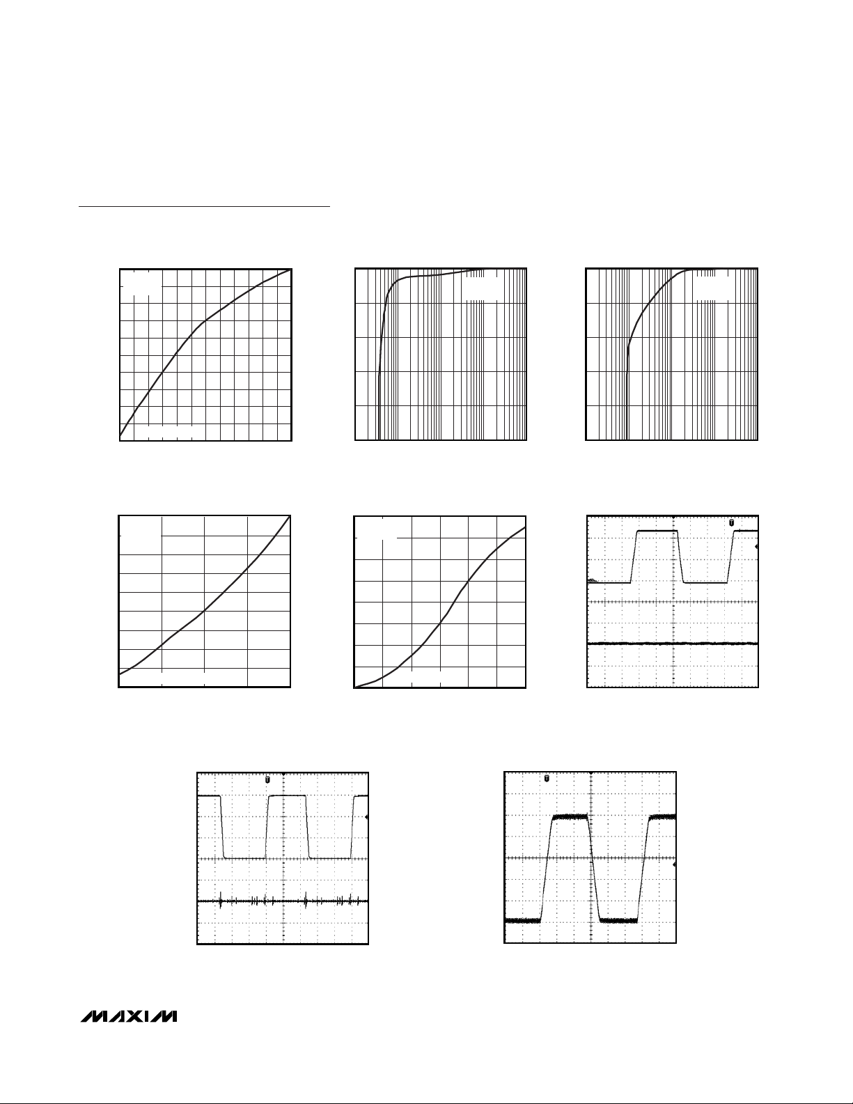
INTEGRAL NONLINEARITY
vs. REFERENCE VOLTAGE
MAX5500 toc01
REFERENCE VOLTAGE (V)
INL (LSB)
3.62.82.01.2
-0.8
-0.6
-0.4
-0.2
0
0.2
-1.0
0.4 4.4
MAX5500
V
DD
= 5V
R
L
= 5k
Ω
INTEGRAL NONLINEARITY
vs. REFERENCE VOLTAGE
MAX5500 toc02
REFERENCE VOLTAGE (V)
INL (LSB)
1.91.40.9
-0.8
-0.6
-0.4
-0.2
0
-1.0
0.4 2.4
MAX5501
V
DD
= 3V
R
L
= 5k
Ω
SUPPLY CURRENT
vs. TEMPERATURE
MAX5500 toc03
TEMPERATURE (°C)
I
DD
(µA)
1109580655035205-10-25-40
860
870
880
890
900
910
850
-55 125
MAX5500
V
DD
= 5V
CODE = FFF hex
Typical Operating Characteristics
(TA = +25°C, unless otherwise noted.)
SCLK Rise to DOUT Valid
Propagation Delay
SCLK Fall to DOUT Valid
Propagation Delay
SCLK Rise to CS Fall Delay t
CS Rise to SCLK Rise Hold
Time
CS Pulse-Width High t
PARAMETER SYMBOL CONDITIONS MIN TYP MAX UNITS
t
D01
t
D02
CS0
t
CS1
CSW
C
LOAD
C
LOAD
= 200pF 80 ns
= 200pF 80 ns
40 ns
40 ns
100 ns
Page 5
MAX5500/MAX5501
Low-Power, Quad, 12-Bit
Voltage-Output DACs with Serial Interface
_______________________________________________________________________________________ 5
Typical Operating Characteristics (continued)
(TA = +25°C, unless otherwise noted.)
SUPPLY CURRENT
vs. TEMPERATURE
830
MAX5501
820
= 3V
V
DD
810
800
790
(µA)
780
DD
I
770
760
750
740
730
CODE = FFF hex
-55 125
TEMPERATURE (°C)
SUPPLY CURRENT
vs. SUPPLY VOLTAGE
940
MAX5500
920
= 5V
V
DD
900
880
860
(µA)
DD
I
840
820
800
780
760
CODE = FFF hex
4.50 5.50
VDD (V)
5.255.004.75
FULL-SCALE ERROR
vs. LOAD
MAX5500 toc05
0
-1
-2
INL (LSB)
-3
-4
-5
0.01 100
0
MAX5500 toc04
-1
-2
INL (LSB)
-3
-4
-5
1109580655035205-10-25-40
0.01 100
LOAD (kΩ)
MAX5500
= 5V
V
DD
1010.1
SUPPLY CURRENT
vs. SUPPLY VOLTAGE
798
MAX5501
= 3V
V
796
MAX5500 toc07
DD
794
792
(µA)
790
DD
I
788
786
784
782
3.0 3.6
CODE = FFF hex
VDD (V)
MAX5500 toc08
3.53.43.1 3.2 3.3
V
DACA CODE SWITCHING FROM 00C hex TO FCC hex
DACB CODE SET TO 800 hex
FULL-SCALE ERROR
vs. LOAD
LOAD (kΩ)
ANALOG CROSSTALK 5V
= 2.5V, RL = 5kΩ, CL = 100pF
REF
10µs/div
MAX5501
= 3V
V
DD
1010.1
MAX5500 toc09
MAX5500 toc06
OUTA
1V/div
OUTB
AC-COUPLED
10mV/div
ANALOG CROSSTALK 3V
= 1.5V, RL = 5kΩ, CL = 100pF
V
REF
DACA CODE SWITCHING FROM 00C hex TO FFF hex
DACB CODE SET TO 800 hex
10µs/div
MAX5500 toc10
OUTA
0.5V/div
OUTB
AC-COUPLED
50mV/div
DYNAMIC RESPONSE 5V
V
= 2.5V, RL = 5kΩ, CL = 100pF
REF
SWITCHING FROM CODE 000 hex TO FB4 hex
OUTPUT AMPLIFIER GAIN = +2
10µs/div
MAX5500 toc11
OUTA
1V/div
Page 6

MAX5500/MAX5501
Low-Power, Quad, 12-Bit
Voltage-Output DACs with Serial Interface
6 _______________________________________________________________________________________
Pin Description
Typical Operating Characteristics (continued)
(TA = +25°C, unless otherwise noted.)
DYNAMIC RESPONSE 3V
MAX5500 toc12
DIGITAL FEEDTHROUGH 3V
(SCLK = 100kHz)
MAX5500 toc13
DIGITAL FEEDTHROUGH 5V
(SCLK = 100kHz)
MAX5500 toc14
OUTA
0.5V/div
V
= 1.5V, RL = 5kΩ, CL = 100pF
REF
SWITCHING FROM CODE 000 hex TO FB4 hex
OUTPUT AMPLIFIER GAIN = +1
10µs/div
V
REF
V
CS
DACA CODE SET TO 800 hex
PIN NAME FUNCTION
1 AGND Analog Ground
2 FBA DAC A Output Amplifier Feedback
3 OUTA DAC A Output Voltage
4 OUTB DAC B Output Voltage
5 FBB DAC B Output Amplifier Feedback
6 REFAB DAC A/DAC B Reference Voltage Input
7 CL
Active-Low Clear Input. CL clears all DACs and registers. CL resets all outputs (OUT_, UPO, and DOUT)
to 0.
8 CS Active-Low Chip-Select Input
9 DIN Serial Data Input
10 SCLK Serial Clock Input
11 DGND Digital Ground
12 DOUT Serial Data Output
13 UPO User-Programmable Logic Output
14 PDL Active-Low Power-Down Lockout. Drive PDL low to lock out software shutdown.
15 REFCD DAC C/DAC D Reference Voltage Input
16 FBC DAC C Output Amplifier Feedback
17 OUTC DAC C Output Voltage
18 OUTD DAC D Output Voltage
19 FBD DAC D Output Amplifier Feedback
20 V
DD
Positive Power Supply
= 1.5V, RL = 5kΩ, CL = 100pF
= V
PDL
4µs/div
= VCL = 3.3V, V
DIN
= 0V
SCLK
1V/div
OUTA
AC-COUPLED
10mV/div
= 2.5V, RL = 5kΩ, CL = 100pF
V
REF
= V
V
CS
PDL
DACA CODE SET TO 800 hex
2µs/div
= VCL = 5V, V
DIN
= 0V
SCLK
2V/div
OUTA
AC-COUPLED
10mV/div
Page 7

MAX5500/MAX5501
Low-Power, Quad, 12-Bit
Voltage-Output DACs with Serial Interface
_______________________________________________________________________________________ 7
Detailed Description
The MAX5500/MAX5501 integrate four 12-bit, voltageoutput digital-to-analog converters (DACs) that are
addressed through a simple 3-wire serial interface. The
devices include a 16-bit data-in/data-out shift register.
Each internal DAC provides a doubled-buffered input
composed of an input register and a DAC register (see
the
Functional Diagram
). The negative input of each
amplifier is externally accessible.
The DACs are inverted rail-to-rail ladder networks that
convert 12-bit digital inputs into equivalent analog output voltages in proportion to the applied reference voltage inputs. DACs A and B share the REFAB input,
while DACs C and D share the REFCD input. The two
reference inputs allow different full-scale output voltage
ranges for each pair of DACs. Figure 1 shows a simplified circuit diagram of one of the four DACs.
Reference Inputs
The two reference inputs accept positive DC and AC
signals. The voltage at each reference input sets the
full-scale output voltage for the two corresponding
DACs. The reference input voltage range is 0V to (V
DD
- 1.4V). The output voltages (V
OUT_
) are represented by
a digitally programmable voltage source as:
V
OUT_
= (V
REF
x NB/4096) x Gain
where NB is the numeric value of the binary input code
(0 to 4095) of the DAC. V
REF
is the reference voltage.
Gain is the externally set voltage gain.
The impedance at each reference input is code-dependent, ranging from a low value of 10kΩ when both
DACs connected to the reference accept an input code
of 555 hex, to a high value exceeding giga-ohms with
an input code of 000 hex. The load regulation of the reference source affects the performance of the devices
as the input impedance at the reference inputs is code
dependent. The REFAB and REFCD reference inputs
provide a 10kΩ guaranteed minimum input impedance.
When the same voltage source drives the two reference
inputs, the effective minimum impedance is 5kΩ. A voltage reference with an excellent load regulation of
0.0002mV/mA, such as the MAX6033, is capable of driving both reference inputs simultaneously at 2.5V.
Driving REFAB and REFCD separately improves reference accuracy.
The REFAB and REFCD inputs enter a high-impedance
state, with a typical input leakage current of 0.02µA,
when the MAX5500/MAX5501 are in shutdown. The reference input capacitance is also code dependent and
typically ranges from 20pF with an input code of all 0s
to 100pF with an input code of all 1s.
Output Amplifiers
All DAC outputs are internally buffered by precision
amplifiers with a typical slew rate of 0.6V/µs. Access to
the inverting input of each output amplifier provides the
greater flexibility in output gain setting/signal conditioning (see the
Applications Information
section).
With a full-scale transition at the output, the typical settling time to within ±0.5 LSB is 12µs when the output is
loaded with 5kΩ in parallel with 100pF. A load of less
than 2kΩ at the output degrades performance. See the
Typical Operating Characteristics
for the output dynamic
responses and settling performances of the amplifiers.
Power-Down Mode
The MAX5500/MAX5501 feature a software-programmable shutdown that reduces supply current to a typical value of 10µA. Drive PDL high to enable the
shutdown mode. Write 1100XXXXXXXXXXXX as the
input-control word to put the device in power-down
mode (Table 1).
In power-down mode, the output amplifiers and the reference inputs enter a high-impedance state.
The serial interface remains active. Data in the input
registers is retained in power-down, allowing the
devices to recall the output states prior to entering shutdown. Start up from power-down either by recalling the
previous configuration or by updating the DACs with
new data. Allow 15µs for the outputs to stabilize when
powering up the devices or bringing the devices out of
shutdown.
OUT_
FB_
SHOWN FOR ALL 1s ON DAC
D0 D9 D10
D11
2R
2R 2R 2R 2R
RRR
REF_
AGND
Figure 1. Simplified DAC Circuit Diagram
Page 8

MAX5500/MAX5501
Low-Power, Quad, 12-Bit
Voltage-Output DACs with Serial Interface
8 _______________________________________________________________________________________
Figure 2. Connections for MICROWIRE
Serial-Interface Configurations
The MAX5500/MAX5501s’ 3-wire serial interface is
compatible with both MICROWIRE (Figure 2) and
SPI/QSPI (Figure 3). The serial input word consists of
two address bits and two control bits followed by 12
data bits (MSB first), as shown in Figure 4. The 4-bit
address/control code determines the MAX5500/
MAX5501s’ response outlined in Table 1. The connection between DOUT and the serial-interface port is not
necessary, but may be used for data echo. Data held in
the shift register can be shifted out of DOUT and
returned to the µP for data verification.
The digital inputs of the MAX5500/MAX5501 are double
buffered. Depending on the command issued through the
serial interface, the input register(s) can be loaded without
affecting the DAC register(s), the DAC register(s) can be
loaded directly, or all four DAC registers can be updated
simultaneously from the input registers (Table 1).
Serial-Interface Description
The MAX5500/MAX5501 require 16 bits of serial data.
Table 1 lists the serial-interface programming commands. For certain commands, the 12 data bits are
don’t-care bits. Data is sent MSB first and can be sent
in two 8-bit packets or one 16-bit word (CS must remain
low until 16 bits are transferred). The serial data is composed of two DAC address bits (A1, A0) and two control
bits (C1, C0), followed by the 12 data bits D11–D0
(Figure 4). The 4-bit address/control code determines:
• The register(s) to be updated
• The clock edge on which data is to be clocked out
through the serial-data output (DOUT)
• The state of the user-programmable logic output
(UPO)
• If the device is to enter shutdown mode (assuming
PDL is high)
• How the device is configured when exiting out of
shutdown mode
DOUT*
DIN
SCLK
CS
MISO*
MOSI
SCK
I/O
SPI/QSPI
PORT
SS
+5V
CPOL = 0, CPHA = 0
*THE DOUT-MISO CONNECTION IS NOT REQUIRED FOR WRITING TO THE
MAX5500/MAX5501, BUT CAN BE USED FOR READBACK PURPOSES.
MAX5500
MAX5501
Figure 3. Connections for SPI/QSPI
MSB.................................................................................................................................LSB
MSB...........................................................................................LSB
16 BITS OF SERIAL DATA
ADDRESS
BITS
CONTROL
BITS
DATA BITS
4 ADDRESS/
CONTROL BITS
D11..............................................................................................D0
A1 A0 C1 C0
12 DATA BITS
Figure 4. Serial-Data Format
SCLK
DIN
MAX5500
MAX5501
*THE DOUT-SI CONNECTION IS NOT REQUIRED FOR WRITING TO THE
MAX5500/MAX5501, BUT CAN BE USED FOR READBACK PURPOSES.
DOUT*
CS
SK
SO
SI*
I/O
MICROWIRE
PORT
Page 9

MAX5500/MAX5501
Table 1. Serial-Interface Programming Commands
Figure 5 shows the serial-interface timing requirements.
The CS input must be low to enable the DAC’s serial
interface. When CS is high, the interface control circuitry
is disabled. CS must go low for at least t
CSS
before the
rising serial clock (SCLK) edge to properly clock in the
first bit. When CS is low, data is clocked into the internal
shift register through the serial data input (DIN) on the
rising edge of SCLK. The maximum guaranteed clock
frequency is 10MHz. Data is latched into the appropriate
input/DAC registers on the rising edge of CS.
The programming command “load-all-dacs-from-shiftregister” allows all input and DAC registers to be simultaneously loaded with the same digital code from the
input shift register. The no operation (NOP) command
leaves the register contents unaffected. This feature is
used in a daisy-chain configuration (see the
Daisy
Chaining Devices
section).
The command to change the clock edge on which serial data is shifted out of DOUT also loads data from all
input registers to their respective DAC registers.
Serial-Data Output (DOUT)
The serial-data output, DOUT, is the internal shift register’s output. The MAX5500/MAX5501 can be programmed so that data is clocked out of DOUT on the
rising edge of SCLK (mode 1) or the falling edge (mode
0). In mode 0, output data at DOUT lags input data at
DIN by 16.5 clock cycles, maintaining compatibility with
MICROWIRE, SPI/QSPI, and other serial interfaces. In
mode 1, output data lags input data by 16 clock cycles.
On power-up, DOUT defaults to mode 0 timing.
User-Programmable Logic Output (UPO)
The user-programmable logic output, UPO, allows an
external device to be controlled through the
MAX5500/MAX5501 serial interface (Table 1).
Low-Power, Quad, 12-Bit
Voltage-Output DACs with Serial Interface
_______________________________________________________________________________________ 9
16-BIT SERIAL WORD
A1 A0 C1 C0
0
0
0
0
1
0
1
0
0
1
1
0
1
0
0
1
1
0
1
0
1
1
1
1
0 1 0 0 XXXXXXXXXXXX Update all DAC registers from their respective input registers (startup).
1 0 0 0 12-bit DAC data Load all DAC registers from shift register (startup).
1 1 0 0 XXXXXXXXXXXX Shutdown (provided PDL = 1)
0 0 1 0 XXXXXXXXXXXX UPO goes low (default)
0 1 1 0 XXXXXXXXXXXX UPO goes high
0 0 0 0 XXXXXXXXXXXX No operation (NOP) to DAC registers
1 1 1 0 XXXXXXXXXXXX Mode 1, DOUT clocked out on SCLK’s rising edge. All DAC registers updated.
1 0 1 0 XXXXXXXXXXXX
D11................D0
MSB LSB
1
12-bit DAC data
1
12-bit DAC data
1
12-bit DAC data
1
12-bit DAC data
12-bit DAC data
1
12-bit DAC data
1
12-bit DAC data
1
12-bit DAC data
1
Load input register A; DAC registers unchanged.
Load input register B; DAC registers unchanged.
Load input register C; DAC registers unchanged.
Load input register D; DAC registers unchanged.
Load input register A; all DAC registers updated.
Load input register B; all DAC registers updated.
Load input register C; all DAC registers updated.
Load input register D; all DAC registers updated.
Mode 0, DOUT clocked out on SCLK’s falling edge. All DAC registers updated
(default).
FUNCTION
Page 10

MAX5500/MAX5501
Low-Power, Quad, 12-Bit
Voltage-Output DACs with Serial Interface
10 ______________________________________________________________________________________
Figure 5. Serial-Interface Timing Diagram
SCLK
DIN
DOUT
t
CSO
t
CSS
t
CL
t
CH
t
CP
t
DO1
t
CSW
t
CS1
t
DO2
t
CSH
t
DS
t
DH
CS
Figure 6. Detailed Serial-Interface Timing Diagram
Power-Down Lockout
(PDL)
Drive power-down lockout, PDL, low to disable software
shutdown. When in shutdown, transitioning PDL from
high to low wakes up the device with the output set to
the state prior to shutdown. Use PDL to asynchronously
wake up the device.
Daisy Chaining Devices
The MAX5500/MAX5501 can be daisy chained by connecting DOUT of one device to DIN of another device
(Figure 7).
Each DOUT output of the MAX5500/MAX5501 includes
an internal active pullup. The sink/source capability of
DOUT determines the time required to discharge/charge
a capacitive load. See the serial-data-out V
OH
and V
OL
specifications in the
Electrical Characteristics.
Figure 8 shows an alternate method of connecting several MAX5500/MAX5501 devices. In this configuration,
the data bus is common to all devices. Data is not shifted through a daisy chain. More I/O lines are required in
this configuration because a dedicated chip-select
input (CS) is required for each IC.
CS
COMMAND
SCLK
1
8
9
EXECUTED
16
A0
DIN
A1 D0
DOUT
(MODE 0)
DOUT
(MODE 1)
A1 D0 A1
A1 D0 A1
C1
A0
C1
MSB FROM
PREVIOUS WRITE
A0
C1
MSB FROM
PREVIOUS WRITE
D11
C0
D11
C0
D11
C0
D10
D9
D10
DATA PACKET (N)
D9
D10
DATA PACKET (N-1)
D9
DATA PACKET (N-1)
D8
D8
D8
D7
D6
D7
D7
D5
D6
D5
D6
D5
D3
D4
D3
D4
D3
D4
D1
D2
D1
D2
DATA PACKET (N)
D1
D2
DATA PACKET (N)
Page 11

MAX5500/MAX5501
Low-Power, Quad, 12-Bit
Voltage-Output DACs with Serial Interface
______________________________________________________________________________________ 11
Figure 7. Daisy Chaining MAX5500/MAX5501
TO OTHER
SERIAL DEVICES
MAX5500
MAX5501
DIN
SCLK
CS
MAX5500
MAX5501
DIN
SCLK
CS
MAX5500
MAX5501
DIN
SCLK
CS
DIN
SCLK
CS1
CS2
CS3
Figure 8. Multiple MAX5500/MAX5501 Devices Sharing a Common DIN Line
MAX5500
SCLK
DIN
CS
SCLK
DIN
CS
MAX5501
DOUT
SCLK
DIN
CS
MAX5500
MAX5501
DOUT
SCLK
DIN
CS
MAX5500
MAX5501
DOUT
TO OTHER
SERIAL DEVICES
Page 12

MAX5500/MAX5501
Low-Power, Quad, 12-Bit
Voltage-Output DACs with Serial Interface
12 ______________________________________________________________________________________
Table 2. Unipolar Code Table
Table 3. Bipolar Code Table
Figure 9. Unipolar Output Circuit
MAX5500
MAX5501
DAC A
DAC B
DAC C
DAC D
V
REFAB
= V
REFCD
= 2.5V
OUTA
10kΩ
10kΩ
10kΩ
10kΩ
10kΩ
10kΩ
10kΩ
10kΩ
OUTB
OUTC
OUTD
DGNDAGND
REFAB
REFCD
REFERENCE INPUTS
+5V
V
DD
FBA
FBB
FBC
FBD
Figure 10. Unipolar Rail-to-Rail Output Circuit
Applications Information
Unipolar Output
For a unipolar output, the output voltages and the reference inputs are of the same polarity. Figure 9 shows
the MAX5500/MAX5501 unipolar output circuit, which is
also the typical operating circuit. Table 2 lists the unipolar output codes.
See Figure 10 for rail-to-rail outputs. Figure 10 shows
the MAX5500/MAX5501 with the output amplifiers configured with a closed-loop gain of +2 to provide 0 to 5V
full-scale range with a 2.5V external reference voltage.
Bipolar Output
Figure 11 shows the MAX5500/MAX5501 configured for
bipolar operation.
V
OUT
= V
REF
[(2NB/4096) - 1]
where NB is the numeric value of the DAC’s binary
input code. Table 3 shows digital codes (offset binary)
and corresponding output voltages for the circuit of
Figure 11.
DAC CONTENTS
MSB LSB
1111 1111 1111 +V
1000 0000 0001 +V
1000 0000 0000 +V
0111 1111 1111 +V
ANALOG OUTPUT
4095
( ——— )
REF
4096
2049
( ——— )
REF
4096
2048 +V
( ——— )= ————
REF
4096 2
2047
( ——— )
REF
4096
REF
MAX5500
MAX5501
REFERENCE INPUTS
REFAB
DAC A
DAC B
REFCD
DAC C
DAC D
+5V
V
DD
DGNDAGND
FBA
OUTA
FBB
OUTB
FBC
OUTC
FBD
OUTD
0000 0000 0001 +V
REF
0000 0000 0000 0V
1
( ——— )
4096
DAC CONTENTS
MSB LSB
1111 1111 1111 +V
1000 0000 0000 0V
0111 1111 1111 -V
1000 0000 0001 +V
0000 0000 0001 -V
0000 0000 0000 -V
Note: 1 LSB = (V
REF
) (
1
4096
ANALOG OUTPUT
REF
)
2047
( ——— )
REF
2048
( ——— )
REF
2048
( ——— )
REF
2048
2047
——— )
(
REF
2048
2048
——— )= -V
(
2048
1
1
REF
Page 13

MAX5500/MAX5501
Low-Power, Quad, 12-Bit
Voltage-Output DACs with Serial Interface
______________________________________________________________________________________ 13
Digitally Programmable Current Source
The circuit of Figure 12 places an npn transistor
(2N3904 or similar) within the op-amp feedback loop to
implement a digitally programmable, unidirectional current source. This circuit drives 4mA to 20mA current
loops, which are commonly used in industrial-control
applications. The output current is calculated with the
following equation:
I
OUT
= (V
REF
/R) x (NB/4096)
where NB is the numeric value of the DAC’s binary input
code and R is the sense resistor shown in Figure 12.
Power-Supply Considerations
On power-up, all input and DAC registers are cleared
(set to zero code) and D
OUT
is in mode 0 (serial data is
shifted out of DOUT on the clock’s falling edge).
For rated MAX5500/MAX5501 performance, limit V
REFAB
/
V
REFCD
to 1.4V below VDD. Bypass VDDwith a 4.7µF
capacitor in parallel with a 0.1µF capacitor to AGND.
Use short lead lengths and place the bypass capacitors as close as possible to the supply inputs.
Grounding and Layout Considerations
Digital or AC transient signals between AGND and
DGND create noise at the analog outputs. Connect
AGND and DGND together at the DAC, and then connect this point to the highest-quality ground available.
Good PCB ground layout minimizes crosstalk between
DAC outputs, reference inputs, and digital inputs.
Reduce crosstalk by keeping analog lines away from
digital lines. Do not use wire-wrapped boards.
Chip Information
PROCESS: BiCMOS
DAC
V
OUT
+5V
-5V
R1 = R2 = 10kΩ ± 0.1%
MAX5500
MAX5501
REF_
R1
R2
FB_
OUT_
Figure 11. Bipolar Output Circuit
DAC_
MAX5500
MAX5501
REF_
OUT_
R
I
OUT
2N3904
V
L
FB_
Figure 12. Digitally Progammable Current Source
Page 14

MAX5500/MAX5501
Low-Power, Quad, 12-Bit
Voltage-Output DACs with Serial Interface
Maxim cannot assume responsibility for use of any circuitry other than circuitry entirely embodied in a Maxim product. No circuit patent licenses are
implied. Maxim reserves the right to change the circuitry and specifications without notice at any time.
14
____________________Maxim Integrated Products, 120 San Gabriel Drive, Sunnyvale, CA 94086 408-737-7600
© 2008 Maxim Integrated Products is a registered trademark of Maxim Integrated Products, Inc.
Package Information
For the latest package outline information and land patterns, go
to www.maxim-ic.com/packages
.
PACKAGE TYPE PACKAGE CODE DOCUMENT NO.
20 SSOP A20-2
21-0056
20
19
18
17
16
15
14
13
1
2
3
4
5
6
7
8
V
DD
FBD
OUTD
OUTCOUTB
OUTA
FBA
AGND
TOP VIEW
FBC
REFCD
PDL
UPOCS
CL
REFAB
FBB
12
11
9
10
DOUT
DGNDSCLK
DIN
SSOP
MAX5500
MAX5501
+
Pin Configuration
 Loading...