

Datasheet MAX5161MEUT, MAX5161LEUT, MAX5160NEUA, MAX5160MEUA, MAX5160LEUA Datasheet (Maxim)
...Page 1
For free samples & the latest literature: http://www.maxim-ic.com, or phone 1-800-998-8800.
For small orders, phone 1-800-835-8769.
General Description
The MAX5160/MAX5161 linear-taper digital potentiometers perform the same function as a mechanical potentiometer or a variable resistor. They consist of a fixed
resistor and a wiper contact with 32 tap points that are
digitally controlled by three lines for the 8-pin MAX5160
or by two lines for the 6-pin MAX5161.
These parts are ideal for applications requiring digitally
controlled resistors. Three resistance values are available for each part type: 50kΩ, 100kΩ, and 200kΩ. A
nominal resistor temperature coefficient of 50ppm/°C
end-to-end and only 5ppm/°C ratiometric makes the
MAX5160 ideal for applications requiring a low-temperature-coefficient variable resistor, such as low-tempco,
adjustable-gain circuit configurations.
The MAX5160 is available in an 8-pin µMAX package,
and the MAX5161 is available in a 6-pin SOT23 package. Both devices are guaranteed over the extendedindustrial temperature range (-40°C to +85°C).
Applications
LCD Screen Adjustment
Volume Control
Mechanical Potentiometer Replacement
Features
♦ 32 Tap Positions
♦ 50kΩ, 100kΩ, and 200kΩ Resistance Values
♦ 400Ω Wiper Resistance
♦ ±25% Resistance Tolerance
♦ 3-Wire Serial Data Input
♦ ±1LSB DNL
♦ ±0.5LSB INL
♦ 100nA Supply Current
♦ Single-Supply Operation: +2.7V to +5.5V
♦ Power-On Reset: Wiper Goes to Midscale
(position 16)
♦ ±2kV ESD Protection
♦ Small-Footprint Packages
6-Pin SOT23 (MAX5161)
8-Pin µMAX (MAX5160)
♦ Glitchless Switching Between the Resistor Taps
MAX5160/MAX5161
Low-Power Digital Potentiometers
________________________________________________________________
Maxim Integrated Products
1
1
2
3
4
8
7
6
5
V
DD
CS
L
WGND
H
U/D
INC
MAX5160
µMAX
TOP VIEW
H
U/DGND
16V
DD
5 INC
L
MAX5161
SOT23-6
2
34
Functional Diagram
19-1435; Rev 1; 4/99
PART
MAX5160NEUA
MAX5160MEUA
PINPACKAGE
8 µMAX
8 µMAX
Pin Configurations
Ordering Information
-40°C to +85°C
-40°C to +85°C
TEMP. RANGE
MAX5160LEUA -40°C to +85°C 8 µMAX
MAX5161NEUT
-40°C to +85°C 6 SOT23-6
MAX5161MEUT -40°C to +85°C 6 SOT23-6
MAX5161LEUT -40°C to +85°C 6 SOT23-6
R
(kΩ)
200
100
50
200
100
50
H
V
DD
GND
CS
INC
U/D
MAX5160
MAX5161
UP/DN
COUNTER
POSITION
DECODER
L
W
Page 2
MAX5160/MAX5161
Low-Power Digital Potentiometers
2 _______________________________________________________________________________________
Note 1: For the MAX5160, linearity is defined in terms of H to L code-dependent resistance.
ABSOLUTE MAXIMUM RATINGS
ELECTRICAL CHARACTERISTICS
(VDD= +2.7V to +5.5V, VH= VDD, VL= 0, TA = T
MIN
to T
MAX
. Typical values are at VDD= 5V, TA= +25°C, unless otherwise noted.)
Stresses beyond those listed under “Absolute Maximum Ratings” may cause permanent damage to the device. These are stress ratings only, and functional
operation of the device at these or any other conditions beyond those indicated in the operational sections of the specifications is not implied. Exposure to
absolute maximum rating conditions for extended periods may affect device reliability.
VDDto GND..............................................................-0.3V to +6V
CS, INC, U/D to GND ...............................................-0.3V to +6V
H, L, W to GND.......................................... -0.3V to (V
DD
+ 0.3V)
Input and Output Latchup Immunity ..............................±200mA
Maximum Continuous Current into H, L, and W
MAX516_ _ E _ _..............................................................±1mA
Continuous Power Dissipation (T
A
= +70°C)
6-Pin SOT23 (derate 8.7mW/°C above +70°C).............696mW
8-Pin µMAX (derate 4.1mW/°C above +70°C)..............330mW
Operating Temperature Range .......................... -40°C to +85°C
Storage Temperature Range.............................-65°C to +150°C
Lead Temperature (soldering, 10sec)............................+300° C
MAX516_ME_ _
MAX516_NE_ _
MAX516_LE_ _
CONDITIONS
ns50t
DI
U/D to INC Setup
ns0t
ID
U/D to INC Hold
ns25t
IH
INC High Period
ns25t
IL
INC Low Period
ns0t
IC
CS to INC Hold Time
ns25t
CI
CS to INC Setup Time
pF5Input Capacitance
µA±1Input Leakage Current
V
0.3 · V
DD
V
IL
Input Low Voltage
V
0.7 · V
DD
V
IH
Input High Voltage
kΩ
37.5 50 62.5
HLEnd-to-End Resistance
LSB±1/2INLIntegral Nonlinearity (Note 1)
%3Resolution
75 100 125
150 200 250
Ω400 1700R
W
Wiper Resistance
LSB+0.1Zero-Scale Error
LSB±1DNLDifferential Nonlinearity (Note 1)
ppm/°C50TC
R
End-to-End Resistor Tempco
ppm/°C5Ratiometric Resistor Tempco
LSB-0.1Full-Scale Error
UNITSMIN TYP MAXSYMBOLPARAMETER
MHz7f
IMAX
INC Frequency
µs1t
IW
Wiper-Settling Time
CS = INC = U/D =
V
DD
or GND
nA135
I
DD
Supply Current
µA0.6 10
V2.7 5.5V
DD
Supply Voltage
VDD= 5V
VDD= 2.7V
pF10C
W
Wiper Capacitance
DIGITAL INPUTS
TIMING CHARACTERISTICS (Figure 6)
POWER SUPPLIES
DC PERFORMANCE
Page 3
MAX5160/MAX5161
Low-Power Digital Potentiometers
_______________________________________________________________________________________
3
0
200
400
600
800
1,000
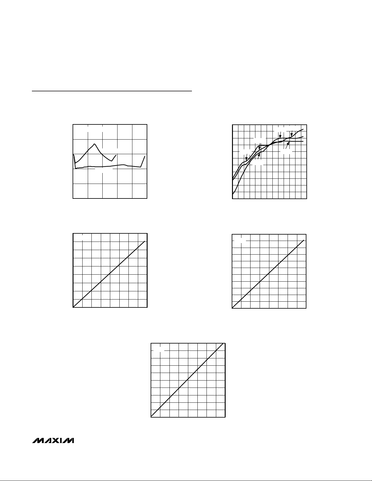
012345
WIPER RESISTANCE
vs. WIPER VOLTAGE
MAX5160/61 toc01
WIPER VOLTAGE (V)
WIPER RESISTANCE (Ω)
R
WMAX
= 574.0804
VDD = +2.7V
VDD = +5V
-0.16
-0.1
-0.12
-0.14
0
-0.02
-0.04
-0.06
-0.08
0.02
0.04
0.06
-40-30-20-100102030405060708090
END-TO-END RESISTANCE % CHANGE
vs. TEMPERATURE
MAX5160/61 toc02
TEMPERATURE (°C)
END-TO-END RESISTANCE % CHANGE
200kΩ
200kΩ
100kΩ
50kΩ
50kΩ
100kΩ
0
50
25
125
100
75
150
175
200
225
1 5 9 131721252933
END-TO-END RESISTANCE
vs. TAP POSITION
MAX5160/61 toc03
TAP POSITION
RESISTANCE (kΩ)
200kΩ
0
20
10
50
40
30
60
70
80
90
100
110
1 5 9 131721252933
END-TO-END RESISTANCE
vs. TAP POSITION
MAX5160/61 toc04
TAP POSITION
RESISTANCE (kΩ)
100kΩ
Typical Operating Characteristics
(VDD= +5V, TA= +25°C, unless otherwise noted.)
0
10
5
25
20
15
30
35
40
45
50
1 5 9 131721252933
END-TO-END RESISTANCE
vs. TAP POSITION
MAX5160/61 toc05
TAP POSITION
RESISTANCE (kΩ)
50kΩ
Page 4

MAX5160/MAX5161
Low-Power Digital Potentiometers
4 _______________________________________________________________________________________
PIN
Typical Operating Characteristics (continued)
(VDD= +5V, TA= +25°C, unless otherwise noted.)
0
0.2
0.1
0.5
0.4
0.3
0.8
0.7
0.6
0.9
-40 0 20-20 40 60 80 100
SUPPLY CURRENT vs. TEMPERATURE
MAX5160/61 toc06
TEMPERATURE (°C)
SUPPLY CURRENT (µA)
VDD = +5V
VDD = +2.7V
1
INC
Wiper Increment Control Input. With CS low, a high-to-low transition increments
(U/D high) or decrements (U/D low) the wiper position.
2
U/D
Up/Down Control Input. With CS low, a high-to-low INC transition increments
(U/D high) or decrements (U/D low) the wiper position.
3 H High Terminal of Resistor
4 GND Ground
8 V
DD
Power Supply
7
CS Chip-Select Input. Drive low to change the wiper position via INC and U/D.
6 L Low Terminal of Resistor
5 W Wiper Terminal of Resistor
Pin Description
NAME FUNCTION
MAX5160
5
4
PIN
2
3
6
—
1
—
MAX5161
2V/div
OUTPUT
50mV/div
INC
TAP-TO-TAP SWITCHING TRANSIENT
W
0V
0V
5µs/div
MAX5160/61 toc07
Page 5

MAX5160/MAX5161
Low-Power Digital Potentiometers
_______________________________________________________________________________________ 5
Detailed Description
The MAX5160/MAX5161 consist of resistor arrays with
31 resistive elements. Thirty-two tap points are accessible to the wiper along the resistor string between H and
L. Logic inputs CS, U/D, and INC determine the position of the wiper. With CS low and U/D high, a high-tolow transition on INC increments the internal counter,
increasing the resistance between W and L. When both
CS and U/D are low, a high-to-low INC transition
decrements the internal counter, decreasing the resistance between W and L. At either end (maximum or minimum positions), additional transitions in the direction of
the end points will not change the counter value (the
counter will not wrap around).
The H and L terminals of the MAX5160 are similar to the
two end terminals of a mechanical potentiometer. The
tap W is equivalent to the variable tap (wiper) of the
potentiometer.
The MAX5161 is similar to the MAX5160 except that CS
internally connects to ground and the wiper terminal (W)
is shorted to the high terminal (H). The MAX5161 acts as
a variable resistor (a potentiometer with the wiper and
one end terminal shorted together).
The MAX5160/MAX5161 feature power-on reset circuitry that sets the wiper position to midscale at power-up.
Applications Information
The MAX5160/MAX5161 are intended for circuits
requiring digitally controlled adjustable voltage or
adjustable gain, such as LCD contrast control, where
voltage biasing adjusts the display contrast.
Controlling a Switch-Mode
LCD Bias Generator
Figure 1 shows an application where the MAX5161 is
used with a MAX1771 to make an adjustable positive
LCD-bias circuit. The output of the MAX1771 is a positive voltage that is digitally controlled through the
MAX5160/MAX5161. Similarly, Figure 2 shows the
application of the MAX5161 in a digitally controlled
negative LCD-bias circuit along with the MAX774/
MAX775/MAX776.
MAX1771
VIN = 5V
REF
SHDN
AGND
GND
N
MTD20N03HDL
7
EXT
CS
FB
L1
22µH
D1
1N5817-22
C4
300µF
C5
C3
0.1µF
5
4
6
1
8
3
2
V+
C1
68µF
V
OUT
= 12V
AT 0.5A
R2
R
SENSE
40mΩ
C2
0.1µF
V
REF
= 1.5V
R1
R
VAR
V
OUT(MAX)
= R2
+ 1
V
REF
R1
V
OUT(MIN)
=
(
R2 )
+ 1
V
REF
R1 + R
VAR(MAX)
MAX5161
Figure 1. Adjustable Positive LCD Bias
MAX774
MAX775
MAX776
OUT V+
SHDN
CS
FB EXT
GND
P
7
8
C2
0.1µF
R3
0.07Ω
R1
R2
R
VAR
C1
150µF
6
5
2
3
1
REF
4
Q1
Si9435
1N5822/
MBR340
L1
22µH
C4*
V
IN
C3
0.1µF
V
OUT
* MAX774 = 330µF, 10V
MAX775, MAX776 = 120µF, 20V
V
OUT(MAX)
= R2
,
V
OUT(MIN)
= R2
V
REF
R1 V
REF
R1 + R
VAR
V
REF
- VFB
5µA (FOR 2% GAIN-SETTING ACCURACY)
R1 + R
VAR
MAX5161
Figure 2. Adjustable Negative LCD Bias
Page 6

MAX5160/MAX5161
Alternative Positive
LCD Bias Control
Alternatively, use an op amp to provide buffering and
gain to the output of the MAX5160/MAX5161. Connect
the MAX5160 to the positive input of a noninverting op
amp (Figure 3) to select a portion of the input signal by
digitally controlling the wiper terminal. Figure 4 shows a
similar circuit for the MAX5161.
Adjustable Gain
Figure 5 shows how to use the MAX5161 to digitally
adjust the gain of a noninverting op amp configuration.
Connect the MAX5161 in series with a resistor to ground
to form the adjustable gain control of a noninverting
amplifier. The MAX5160/MAX5161 have a low 5ppm/°C
ratiometric tempco that allows for a very stable adjustable gain configuration over temperature.
Serial Interface
Figure 6 is the serial-interface timing diagram.
Low-Power Digital Potentiometers
6 _______________________________________________________________________________________
GAIN 6
30V
W
L
H
INC
CS
GND
+5V
+5V
V
OUT
V
DD
U/D
MAX5160
Figure 3. MAX5160 Positive LCD Bias Control
GAIN 6
30V
L
H
GND
+5V+5V
V
OUT
V
DD
INC
U/D
MAX5161
Figure 4. MAX5161 Positive LCD Bias Control
V
CC
L
H
GND
V
IN
+5V
a)
b)
V
OUT
V
DD
INC
U/D
V
CC
L
H
W
V
IN
V
OUT
MAX5161
MAX5160
Figure 5. Adjustable Gain Circuit: a) MAX5161; b) MAX5160
Page 7

Chip Information
TRANSISTOR COUNT: 969
MAX5160/MAX5161
Low-Power Digital Potentiometers
_______________________________________________________________________________________ 7
H +L
↓
H
L —L
↓
OL
↑
L OL
↑
R
W
O
INC
X
U/D
xx-X
CS
H
CS
Figure 6. Serial-Interface Timing Diagram
Truth Table
X =
Don’t care
O =
Previous state
+ =
Increment
— =
Decrement
↓
= High-to-Low Transition
↑ =
Low-to-High Transition
INC
U/D
W
t
CI
t
IL
t
DI
t
ID
t
IW
t
IC
t
IH
Page 8

MAX5160/MAX5161
Low-Power Digital Potentiometers
Maxim cannot assume responsibility for use of any circuitry other than circuitry entirely embodied in a Maxim product. No circuit patent licenses are
implied. Maxim reserves the right to change the circuitry and specifications without notice at any time.
8
_____________________Maxim Integrated Products, 120 San Gabriel Drive, Sunnyvale, CA 94086 408-737-7600
© 1999 Maxim Integrated Products Printed USA is a registered trademark of Maxim Integrated Products.
Package Information
8LUMAXD.EPS
6LSOT.EPS
 Loading...