

Page 1
________________General Description
The MAX5140 is a monolithic, 8-bit digital-to-analog
converter (DAC) capable of accepting video data at
400Msps. Complete with video controls (sync, blank,
reference white (force high), and bright), the MAX5140
directly drives doubly terminated 50Ω or 75Ω loads to
standard composite video levels. Standard setup level
is 7.5IRE. The MAX5140 includes an internal precision
bandgap reference that can drive two other MAX5140s
in an RGB graphics system.
The MAX5140 is available in a 24-pin PDIP package in
the -20°C to +85°C industrial temperature range.
________________________Applications
Raster Graphics
High-Resolution Color or Monochrome Displays
to 2k x 2k Pixels
Medical Electronics: CAT, PET, and MR Imaging
Displays
CAD/CAE Workstations
Solids Modeling
General-Purpose, High-Speed Digital-to-Analog
Conversion
Digital Synthesizers
Automated Test Equipment
Digital Transmitters/Modulators
____________________________Features
♦ 400Msps Nominal Conversion Rate
♦ RS-343-A Compatible
♦ Complete Video Controls: Sync, Blank, Bright,
and Reference White (force high)
♦ ECL Compatible
♦ Single Power Supply
♦ Registered Data and Video Controls
♦ Differential Current Outputs
♦ Stable On-Chip Bandgap Reference
♦ 50Ω and 75Ω Output Drive
♦ ESD-Protected Data and Control Inputs
MAX5140
8-Bit, Ultra-High-Speed DAC
________________________________________________________________
Maxim Integrated Products
1
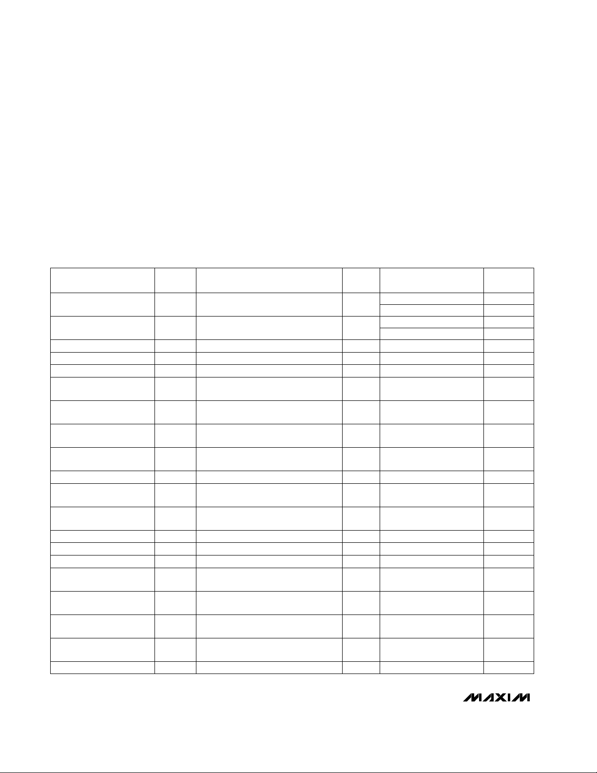
Sync, Blank, Bright, Ref - White
D0 - D3
D4 - D7
(MSBs)
4 To 15
Decode
Output
Current
Switches
Out +
Out -
Bandgap
Reference
Video Controls In
Video Data In
Feedthrough
Convert
Ref In
Ref Out
I
Set
Video Data In
4
4
4
4
2
4
Ref
Buffer
Register
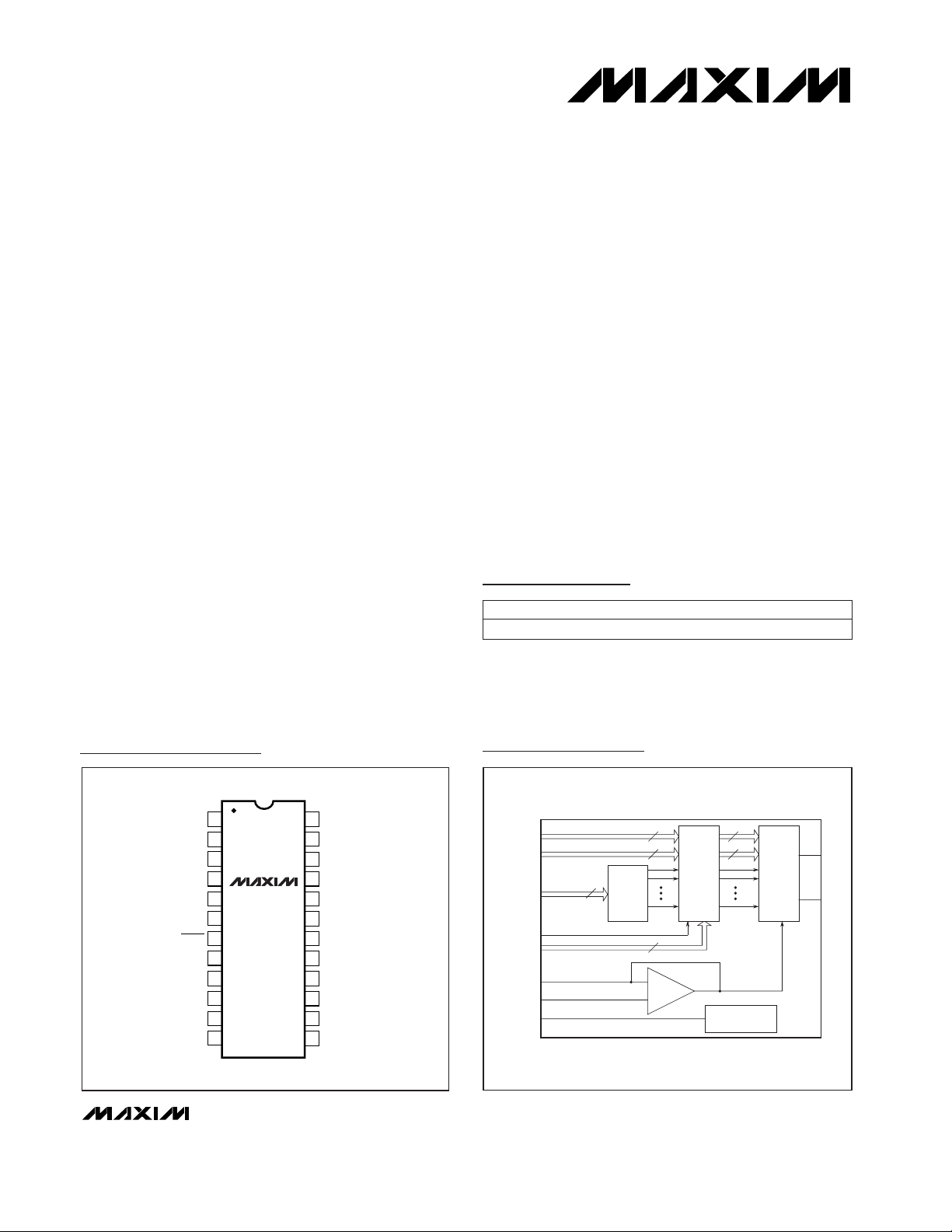
Pin Configuration
24
23
22
21
20
19
18
17
1
2
3
4
5
6
7
8
D4
D5
D6
D7D0
D1
D2
D3
TOP VIEW
V
EE
Out+
OutV
CC
FT
CONV
CONV
V
EE
16
15
14
13
9
10
11
12
I
Set
Ref In
Ref Out
SyncBRT
Blank
FH
V
CC
DIP
MAX5140
Functional Diagram
19-1205; Rev 2; 5/98
PART
MAX5140IPG -20°C to +85°C
TEMP. RANGE PIN-PACKAGE
24 Plastic DIP
Ordering Information
For free samples & the latest literature: http://www.maxim-ic.com, or phone 1-800-998-8800.
For small orders, phone 408-737-7600 ext. 3468.
Page 2
MAX5140
8-Bit, Ultra-High-Speed DAC
2 _______________________________________________________________________________________
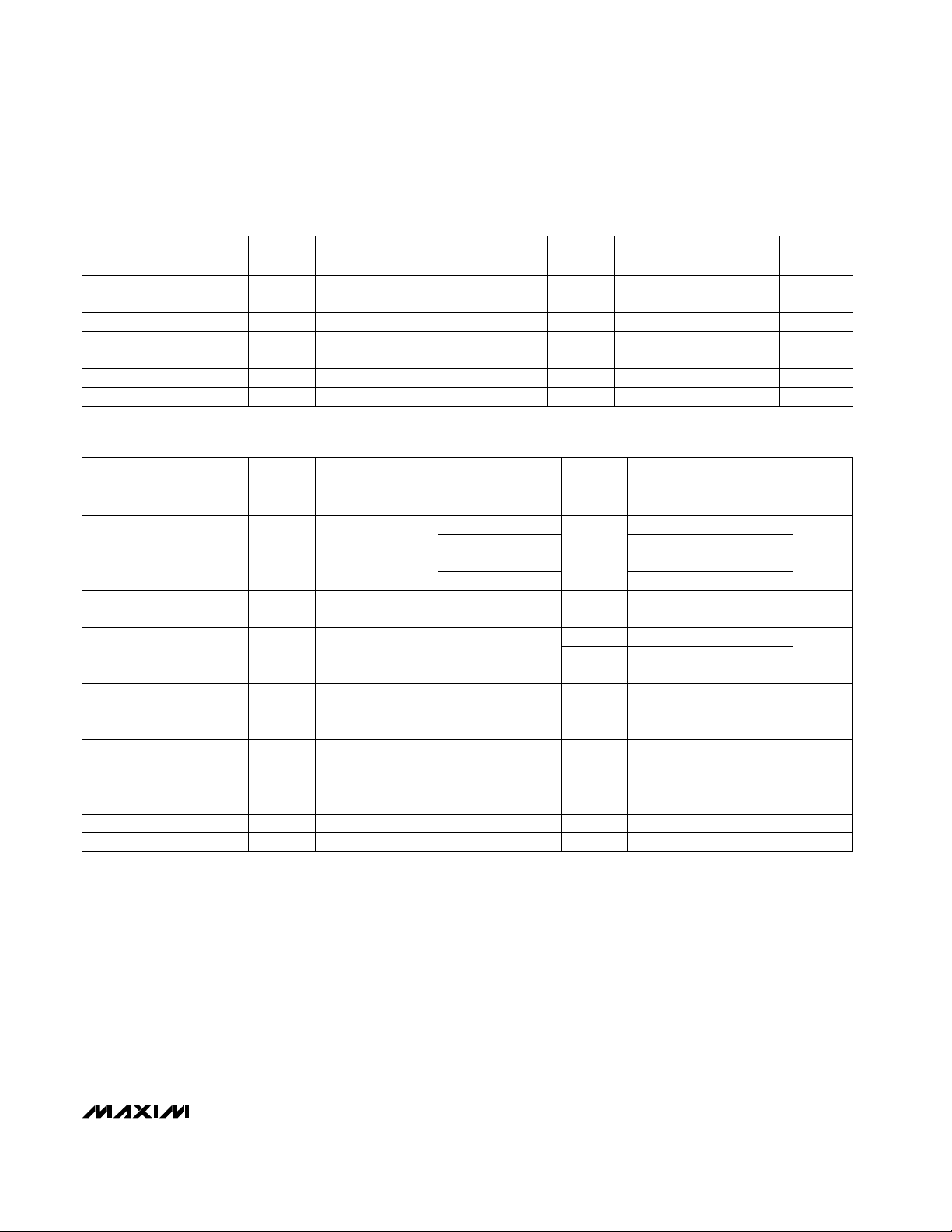
ABSOLUTE MAXIMUM RATINGS
DC ELECTRICAL CHARACTERISTICS
(VCC= ground, VEE= -5.2V ±0.3V, CC= 0pF, I
SET
= 1.105mA, TA= T
MIN
to T
MAX
, unless otherwise noted.)
Stresses beyond those listed under “Absolute Maximum Ratings” may cause permanent damage to the device. These are stress ratings only, and functional
operation of the device at these or any other conditions beyond those indicated in the operational sections of the specifications is not implied. Exposure to
absolute maximum rating conditions for extended periods may affect device reliability.
Supply Voltage
V
EE
(measured to VCC)..........................................-7.0V to 0.5V
Input Voltages
CONV, Data, and Controls (measured to V
CC
)........VEEto 0.5V
Ref+ (measured to V
CC
) ..........................................VEEto 0.5V
Ref- (measured to V
CC
)............................................VEEto 0.5V
Operating Temperature Ranges
Ambient .............................................................-20°C to +85°C
Junction..........................................................................+175°C
Lead Temperature (soldering, 10sec).............................+300°C
Storage Temperature Range.............................-60°C to +150°C
CONDITIONS
V0.4 1.2
Convert Voltage,
Differential
V-0.5 -2.5
Convert Voltage,
Common-Mode Range
V-1.5V
IL
Input Voltage, Logic Low
V-1.0V
IH
Input Voltage, Logic High
LSB0.05 0.5I
OS
Output Offset Current
mA-45I
O-(MAX)
Maximum Current,
Negative Output
mA45I
O+(MAX)
Maximum Current,
Positive Output
pF9C
OUT
Output Capacitance
kΩ20R
OUT
Equivalent Output
Resistance
V-1.2 1.5
Compliance Voltage,
Negative Output
% Full Scale-6.5 6.5Gain Error
ppm/°C100Bandgap Tempco
pF5C
REF
Input Capacitance,
I
SET
, Ref Out
V-1.2 1.5
Compliance Voltage,
Positive Output
UNITSMIN TYP MAXSYMBOLPARAMETER
IV
IV
IV
V
VI
VI
VI
VI
VI
V
V
VI
VI
IV
TEST
LEVEL
µA35 120I
IL
Input Current, Logic Low,
Data and Controls
VI
µA40 120I
IH
Input Current, Logic High,
Data and Controls
VI
µA2 60I
CONV
Input Current, Convert VI
1.0mA < I
SET
< 1.3mA
% Full Scale -0.37 0.37
ILEIntegral Linearity Error VI
1.0mA < I
SET
< 1.3mA
% Full Scale -0.2 0.2
DLEDifferential Linearity Error VI
-0.95 0.95
-0.5 0.5
LSB
LSB
ppm/°C150Gain-Error Tempco V
Page 3
MAX5140
8-Bit, Ultra-High-Speed DAC
_______________________________________________________________________________________ 3
DC ELECTRICAL CHARACTERISTICS (continued)
(VCC= ground, VEE= -5.2V ±0.3V, CC= 0pF, I
SET
= 1.105mA, TA= T
MIN
to T
MAX
, unless otherwise noted.)
AC ELECTRICAL CHARACTERISTICS
(RL= 37.5Ω, CL= 5pF, I
SET
= 1.105mA, TA= +25°C, unless otherwise noted.)
CONDITIONS
mA155 220I
EE
Supply Current
V-1.3 -1.2 -1.0V
REF
Reference Voltage
(measured to V
CC
)
pF3C
IN
Input Capacitance, Data
and Controls
µA/V-120 20 120Power-Supply Sensitivity
UNITSMIN TYP MAXSYMBOLPARAMETER
VI
VI
V
VI
TEST
LEVEL
TA= T
MIN
to T
MAX
10% to 90% G.S.
To 0.2% G.S.
TA= T
MIN
to T
MAX
CONDITIONS
Msps385 400Maximum Conversion Rate
ns
3.2 6
t
DST
Data to Output Delay,
Transparent Mode
ps
900
t
R
Rise Time
ns
4
t
SI
Current-Settling Time,
Clocked Mode
ns
2.2 4
t
DSC
Clock to Output Delay,
Clocked Mode
UNITSMIN TYP MAXSYMBOLPARAMETER
IV
III
IV
V
III
TEST
LEVEL
Area = 1/2VT pV-s4Glitch Energy V
MHz1.25-3dBReference Bandwidth V
ns1.3
t
PWH
,
t
PWL
Convert Pulse Width III
ns0.5t
H
Hold Time, Data and
Controls
III
ns1.0t
S
Setup Time, Data and
Controls
III
dB-48Clock Feedthrough III
20% to 80% G.S. V/µs700Slew Rate V
µA-50I
REF
Reference Output Current VI
600
IV
IV
4.5
6
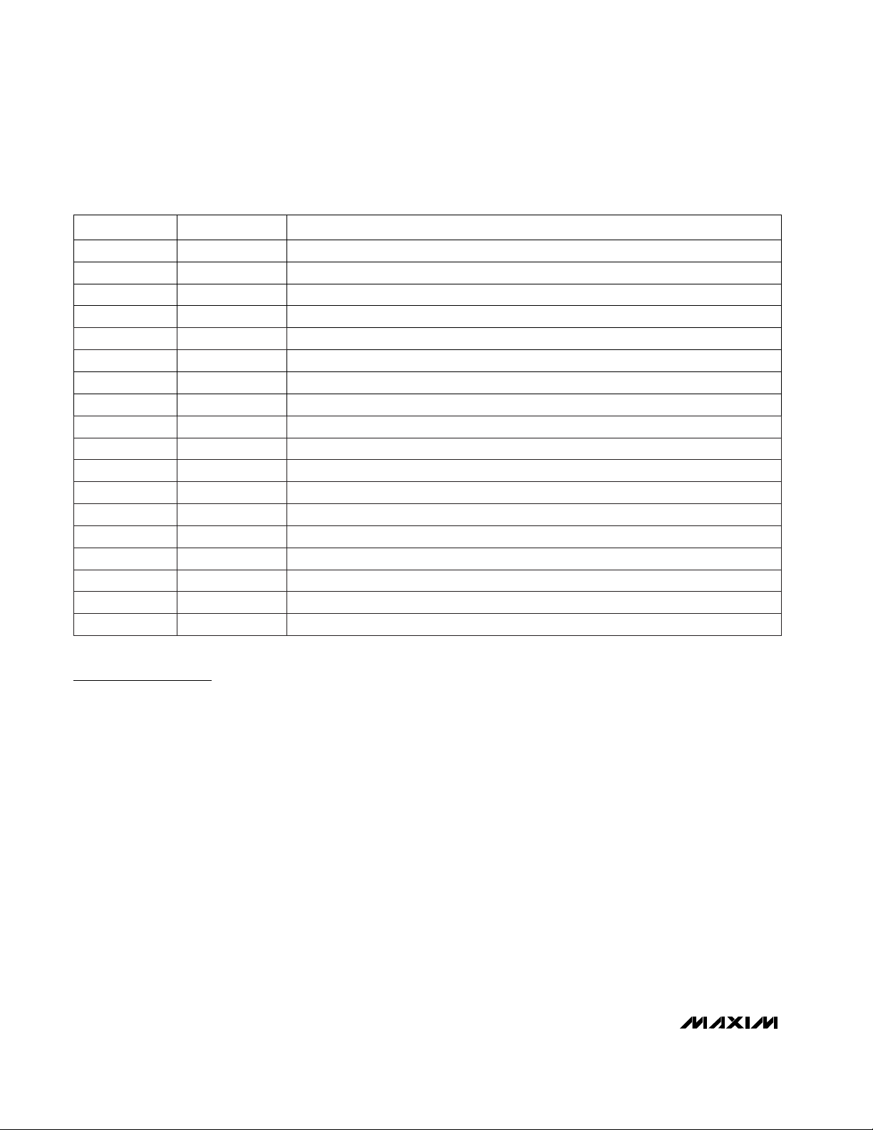
TEST-LEVEL CODES
All electrical characteristics are subject to
the following conditions:
All parameters having min/max specifications are guaranteed. The Test Level column
indicates the specific device testing actually
performed during production and Quality
Assurance inspection. Any blank section in
the data column indicates that the specification is not tested at the specified condition.
Unless otherwise noted, all tests are pulsed
tests; therefore, T
j
= TC= TA.
TEST LEVEL
I
II
III
IV
V
VI
TEST PROCEDURE
100% production tested at the specified temperature.
100% production tested at T
A
= +25°C, and sample-
tested at the specified temperatures.
QA sample tested at only the specified temperatures.
Parameter is guaranteed (but not tested) by design
and characterization data.
Parameter is a typical value for reference.
100% production tested at T
A
= +25°C. Parameter is
guaranteed over specified temperature range.
RL= 25Ω
RL= 25Ω 3
Page 4
MAX5140
8-Bit, Ultra-High-Speed DAC
4 _______________________________________________________________________________________
______________________________________________________________Pin Description
Detailed Description
The MAX5140 is an ultra-high-speed video digital-toanalog converter (DAC) capable of up to 400Msps conversion rates. This high speed makes the device
suitable for driving 2048 x 2048 pixel displays at 60Hz
to 90Hz update rates.
In addition, the MAX5140 includes an internal bandgap
reference, which may be used to drive two other
MAX5140s, if desired.
The MAX5140 has ECL logic-level-compatible video
control and data inputs. The complementary analog
output currents produced by the devices are proportional to the product of the digital control and data
inputs in conjunction with the analog reference current.
The MAX5140 is segmented so that the input data’s
four MSBs are separated into a parallel thermometer
code. From here, fifteen identical current sinks are driven to fabricate sixteen coarse output levels. The
remaining four LSBs drive four binary-weighted current
switches.
MSB currents are then summed with the LSBs that contribute one-sixteenth of full-scale to provide the 256 distinct analog output levels.
The video-control inputs drive weighted current sinks,
which are added to the output current to produce composite video-output levels. These controls (sync, blank,
reference white (force high), and bright) are required in
video applications.
A feature that similar video DACs do not have is feedthrough control. The feedthrough pin (FT) allows registered or unregistered operation of the video control and
data inputs. In registered mode, the composite functions are latched to the pixel data to prevent screenedge distortions (generally found on unregistered video
DACs).
PIN
Data Bits 3, 2, and 1D3, D2, D11, 2, 3
FUNCTIONNAME
Data Bit 0 (LSB)D04
Convert Clock InputCONV6
Negative SupplyV
EE
5, 20
Register Feedthrough ControlFT8
Data Force-High ControlFH10
Positive SupplyV
CC
9, 17
Convert-Clock-Input Complement
CONV
7
Video Bright InputBRT12
Reference OutputRef Out14
Video Sync InputSync13
Reference CurrentI
Set
16
Output Current NegativeOut-18
Reference InputRef In15
Video Blank InputBlank11
Data Bits 6, 5, and 4D6, D5, D422, 23, 24
Data Bit 7 (MSB)D721
Output Current PositiveOut+19
Page 5

MAX5140
8-Bit, Ultra-High-Speed DAC
_______________________________________________________________________________________ 5
Figure 1. Typical Interface Circuit
Applications Information
General
Figure 1 shows a typical interface circuit using the
MAX5140 in a color-raster application. The MAX5140
requires few external components and is extremely
easy to use. The MAX5140’s ultra-high operating
speeds require good circuit layout, supply decoupling,
and proper transmission-line design. For best performance, note the following considerations.
Input Considerations
Video-input data and controls can be directly connected to the MAX5140. Note that all ECL inputs are
terminated as closely to the device as possible to
reduce ringing, crosstalk, and reflections. Maxim recommends that stripline or microstrip techniques be
used for all ECL interfaces. A convenient and commonly used microstrip impedance is about 130Ω, which is
easily terminated using a 330Ω resistor to V
EE
and a
220Ω resistor to ground. This arrangement gives a
Thevenin-equivalent termination of 130Ω to -2V without
the need for a -2V supply. Standard single in-line package (SIP) 220/330 resistor networks are available for
this purpose.
Figure 2 shows equivalent input circuits.
*An external reference can be used, or the Ref Out reference
can drive three MAX5140s.
Page 6

Output Considerations
The analog outputs are designed to directly drive a
doubly terminated 50Ω or 75Ω load-transmission system as shown. The MAX5140 output source impedances are high-impedance current sinks. The load
impedance (RL) must be 25Ω or 37.5Ω to attain standard RS-343-A video levels. Any deviation from this
impedance affects the resulting video output levels proportionally. As with the data interface, it is important
that all analog transmission lines have matched impedance throughout, including connectors and transitions
between printed wiring and coaxial cable. The combination of matched source-termination resistor RSand
load terminator R
L
minimizes reflections of both forward
and reverse traveling waves in the analog transmission
system.
Power Considerations
The MAX5140 has two analog power-supply pins and
operates from a standard -5.2V single supply. Proper
supply bypassing augments the MAX5140’s inherent
supply-noise-rejection characteristics. As shown
in Figure 1, each supply pin should be bypassed as
close to the device as possible with 0.01µF and 10µF
capacitors.
MAX5140
8-Bit, Ultra-High-Speed DAC
6 _______________________________________________________________________________________
Figure 2. Equivalent Input Circuits—Data, Clock, Controls, and Reference
I
Bias
V
EE
Conv
Conv
I
Bias
V
EE
V
CC
Reference
Segment
Switch
Ref In
I
Set
I
Bias
I
Bias
80 kΩ
V
EE
V
Data and
Controls
Page 7

This device also has two analog ground pins (VCC). Tie
both ground pins to the analog ground plane. All power
and ground pins must be connected in any application.
If a +5V power source is required, the VCCground
pins become the positive supply pins, while the V
EE
supply pins become the ground pins. The relative
polarities of the other input and output voltages must
be maintained.
Reference Considerations
The MAX5140 has two reference inputs (Ref In and I
Set
)
and one reference output (Ref Out). The input pins are
connected to the inverting and noninverting inputs of
an internal amplifier that serves as a reference buffer.
The buffer amplifier’s output is the reference for the current sinks. The amplifier feedback loop is connected
around one of the current sinks to achieve better accuracy. (See Figure 3.)
Since the analog output currents are proportional to the
digital input data and I
Set
, full-scale output can be
adjusted by varying the reference current. I
Set
is con-
trolled through the MAX5140’s I
Set
input. Figure 1
shows the method and the necessary equations for setting I
Set
. The MAX5140 can use an external negativevoltage reference. The external reference must be stable to achieve a satisfactory output, and Ref In should
be driven through a resistor to minimize offsets caused
by bias current. To change the full-scale output,
vary the value for I
Set
with the 500Ω to 1kΩ trimmer.
A double 50Ω load (25Ω) can be driven if I
Set
is
increased by 50% for doubly terminated 75Ω video
applications.
Data Inputs and Video Controls
The MAX5140 has standard, single-ended data inputs.
The inputs are registered to produce the lowest differential data-propagation delay (skew) to minimize glitching. Also, four video-control inputs generate composite
video outputs: sync, blank, bright, and reference white
(force high). Feedthrough control is also provided. All
of the controls and data inputs are ECL compatible. In
addition, all have internal pulldown resistors to leave
them at a logic low so the pins are inactive when not
used. This is useful if the devices are applied as standard DACs without the need for video controls, or if
fewer than eight bits are used.
The MAX5140 is usually configured in synchronous
mode. In this mode, the controls and data are synchronized to prevent pixel dropout. This reduces screenedge distortions and provides the lowest output noise
while maintaining the highest conversion rate. With the
FT control open (low), each rising edge of the convert
clock (CONV) latches decoded data and control values
into a D-type internal register. The switched-current
sinks convert the registered data into the appropriate
analog output. When FT is tied high, the control inputs
and data are not registered. The analog output asynchronously tracks the input data and video controls.
Feedthrough itself is asynchronous and is usually used
as a DC control.
MAX5140
8-Bit, Ultra-High-Speed DAC
_______________________________________________________________________________________ 7
Figure 3. Reference Buffer and DAC Output Circuit
Page 8

MAX5140
To be registered synchronously, control and data inputs
must be present at the input pins for a specific setup
time (ts) before and a specific hold time (tH) after
CONV’s rising edge. Setup and hold times are not important in asynchronous mode. The minimum pulse widths
high (t
PWH
) and low (t
PWL
), as well as settling time,
become the limiting factors (Figure 4).
The video controls produce the output levels needed
for horizontal blanking, frame synchronization, etc., to
be compatible with video-system standards as
described in RS-343-A. Table 1 shows the videocontrol effects on the analog output. Internal logic governs blank, sync, and force high so that they override
the data inputs as needed in video applications. Sync
overrides both the data and other controls to produce
full negative video output (Figure 5).
Reference-white, video-level output is provided by
force high, which drives the internal digital data to fullscale output (100IRE units). Bright gives an additional
10% of full-scale value to the output level. This function
can be used in graphic displays for highlighting menus,
cursors, or warning messages. If the devices are used
in nonvideo applications, the video controls can be left
open.
Convert Clock
For best performance, the clock should be differentially
ECL driven by using CONV and CONV (Figure 6).
Driving the clock in this manner minimizes clock noise
and power-supply/output intermodulation. The clock’s
rising edge synchronizes the data and control inputs to
the MAX5140. Since CONV determines the actual
switching threshold of CONV, the clock can be driven
single-ended by connecting a bias voltage to CONV.
This bias voltage sets the converter clock’s switching
threshold.
Analog Outputs
The MAX5140 has two analog outputs that are highimpedance, complementary current sinks. The outputs
vary in proportion to the input data, controls, and reference-current values so that the full-scale output can be
changed by setting I
Set
.
8-Bit, Ultra-High-Speed DAC
8 _______________________________________________________________________________________
-1.3 V
CONV
CONV
1/2 LSB
t
PWL
t
H
t
S
t
PWH
t
SI
OUT +
OUT -
1/2 LSB
-1.3 V
t
DSC
t
DST
Data Control
Inputs
Figure 4. Timing Diagram
Page 9

MAX5140
8-Bit, Ultra-High-Speed DAC
_______________________________________________________________________________________ 9
1 X0 X X 20.83 -0.781 0 Blank Level
0 10 1 X 0.00
BLANK
X
0.000 110 Enhanced High Level
SYNC
REF
WHITE
X1
0 00 0 111... 1.95
0
-0.073 100 Normal High Level
0 00 0 000...
BRIGHT
X
19.40 -0.728 7.5 Normal Low Level
10 0 X 1.95 -0.073 100 Normal High Level
DATA
INPUT
X
0 00 1 111... 0.00 0.000 110
OUT- (mA)
28.57
Enhanced High Level
0 00 1 000... 17.44 -0.654 17.5 Enhanced Low Level
OUT- (V)
-1.071
OUT- (IRE)
-40
DESCRIPTION
Sync Level
Table 1. Video-Control Operation (output values for setup: 10IRE, 75Ω standard load)
256 Gray Levels
Normal Low (Black)
Sync
Video
Blank
Bright
Normal High (White)
110
100
7.5
0
-40
IRE
0 mV
-73 mV
-728 mV
-781 mV
-1071 mV
Figure 5. Video-Output Waveform for Standard Load
Page 10

MAX5140
8-Bit, Ultra-High-Speed DAC
10 ______________________________________________________________________________________
Figure 6. CONV, CONV Switching Levels
In video applications, the outputs can drive a doubly
terminated 50Ω or 75Ω load to standard video levels. In
the standard configuration shown in Figure 7, the output voltage is the product of the output current and
load impedance and is between 0V and -1.07V. Out(Figure 5) provides a video output waveform with the
Sync pulse bottom at -1.07V. Out+ is inverted with Sync
up.
Typical RGB Graphics System
In an RGB graphics system, the color displayed is
determined by the combined intensities of the red,
green, and blue (RGB) DAC outputs. A change in gain
or offset in any of the RGB outputs affects the apparent
hue displayed on the CRT screen. Thus, it is very
important that the DAC’s outputs track each other over
a wide range of operating conditions. Since the DAC
output is proportional to the product of the reference
and digital input code, use a common reference to
drive all three DACs in an RGB system to minimize
RGB DAC-to-DAC mismatch and improve TC tracking.
The MAX5140 contains an internal precision-bandgap
reference that completely eliminates the need for an
external reference. The reference can supply up to
50µA to an external load, such as two other DAC reference inputs.
The circuits shown in Figure 8 show how a single
MAX5140 can be used as a master reference in a system with multiple DACs (such as RGB). The other DACs
are simply slaved from the MAX5140’s reference
output.
Page 11

MAX5140
8-Bit, Ultra-High-Speed DAC
______________________________________________________________________________________ 11
MAX5140
Figure 7. Standard Load (a) and Test Load (b)
MAX5140
(MASTER)
MAX5140
(SLAVE)
MAX5140
(SLAVE)
Figure 8. Typical RGB Graphics System
a)
b)
Page 12

MAX5140
8-Bit, Ultra-High-Speed DAC
________________________________________________________Package Information
PDIPW.EPS
Maxim cannot assume responsibility for use of any circuitry other than circuitry entirely embodied in a Maxim product. No circuit patent licenses are
implied. Maxim reserves the right to change the circuitry and specifications without notice at any time.
12
____________________Maxim Integrated Products, 120 San Gabriel Drive, Sunnyvale, CA 94086 408-737-7600
© 1998 Maxim Integrated Products Printed USA is a registered trademark of Maxim Integrated Products.
 Loading...