

Page 1
General Description
The MAX4959/MAX4960 overvoltage protection controllers protect low-voltage systems against high-voltage faults of up to +28V. When the input voltage
exceeds the overvoltage lockout (OVLO) threshold,
these devices turn off an external pFET to prevent damage to the protected components. The undervoltage
lockout (UVLO) threshold holds the external pFET off
until the input voltage rises to the correct level. An additional safety feature latches off the pFET when an incorrect low-power adapter is plugged in.
The MAX4959/MAX4960 control an external battery
switchover pFET (P2) (see Figures 4 and 6) that switches
in the battery when the AC adapter is unplugged. The
undervoltage and overvoltage trip levels can be adjusted
with external resistors.
The input is protected against ±15kV HBM ESD when
bypassed with a 1µF ceramic capacitor to ground. All
devices are available in a small 10-pin (2mm x 2mm)
µDFN and 10-pin µMAX packages and are specified for
operation over the extended -40°C to +85°C temperature
range.
Applications
Notebooks
Laptops
Camcorders
Ultra-Mobile PCs
Features
o Overvoltage Protection Up to +28V
o ± 2.5% Accurate Externally Adjustable
OVLO/UVLO Thresholds
o Battery Switchover pFET Control
o Protection Against Incorrect Power Adapter
o Low (100µA Typ) Supply Current
o 25ms Input Debounce Timer
o 25ms Blanking Time
o 10-Pin (2mm x 2mm) µDFN and 10-Pin µMAX
Packages
MAX4959/MAX4960
High-Voltage OVP with Battery Switchover
________________________________________________________________
Maxim Integrated Products
1
19-0874; Rev 0; 7/07
For pricing delivery, and ordering information please contact Maxim Direct at 1-888-629-4642,
or visit Maxim’s website at www.maxim-ic.com.
Ordering Information
PART TEMP RANGE
PINPACKAGE
TOP
MARK
PKG
CODE
MAX4959ELB+
-40°C to +85°C
10 μDFN AAO L1022-1
MAX4959EUB+* -40°C to +85°C 10 μMAX — U10-1
MAX4960ELB+ -40°C to +85°C 10 μDFN AAP L1022-1
MAX4960EUB+* -40°C to +85°C 10 μMAX — U10-1
123
10 9 8
45
76
GATE2
GND
V
DD
N.C.
GATE1
OVS
IN
N.C.
(SOURCE1)
MAX4959
MAX4960
µDFN
TOP VIEW
CB
UVS
+
1
2
3
4
5
6
7
8
9
10
GATE2
GND
V
DD
N.C.
GATE1
OVS
( ) MAX4960 ONLY.
IN
N.C.
(SOURCE1)
MAX4959
MAX4960
µMAX
CB
UVS
+
Pin Configurations
Typical Operating Circuits appear at end of data sheet.
+
Denotes a lead-free package.
*
Future product—Contact factory for availability.
Page 2

MAX4959/MAX4960
High-Voltage OVP with Battery Switchover
2 _______________________________________________________________________________________
ABSOLUTE MAXIMUM RATINGS
ELECTRICAL CHARACTERISTICS
(V
IN
= +19V, TA= -40°C to +85°C, unless otherwise noted, C
VDD
= 100nF. Typical values are at TA = +25°C.) (Note 1)
Stresses beyond those listed under “Absolute Maximum Ratings” may cause permanent damage to the device. These are stress ratings only, and functional
operation of the device at these or any other conditions beyond those indicated in the operational sections of the specifications is not implied. Exposure to
absolute maximum rating conditions for extended periods may affect device reliability.
IN, SOURCE1, GATE1, GATE2, to GND ................-0.3V to +30V
V
DD
to GND..............................................................-0.3V to +6V
UVS, OVS, CB to GND .............................................-0.3V to +6V
Continuous Power Dissipation (T
A
= +70°C)
10-pin µDFN (derate 5.0mW/°C above +70°C) ...........403mW
10-pin µMAX (derate 5.6mW/°C above +70°C) ...........444mW
Operating Temperature Range ...........................-40°C to +85°C
Junction Temperature......................................................+150°C
Storage Temperature Range .............................-65°C to +150°C
Lead Temperature (soldering, 10s) .................................+300°C
PARAMETER SYMBOL CONDITIONS MIN TYP MAX UNITS
IN
Input Voltage Range V
Overvoltage Adjustable Trip
Range
Overvoltage Comp Reference OV
OVS Input Leakage Current OVI
Overvoltage Trip Hysteresis OV
Undervoltage Adjustable Trip
Range
Undervoltage Comp Reference UV
UVS Input Leakage Current UVI
Undervoltage Trip Hysteresis UV
Internal Undervoltage Trip Level INTUV
Internal Undervoltage Trip
Hysteresis
IN
OVLO (Note 2) 6 28 V
VIN rising edge 1.18 1.228 1.276 V
REF
LKG
HYS
UVLO (Note 2) 5 28 V
VIN falling edge 1.18 1.228 1.276 V
REF
LKG
HYS
REFVIN
INTUV
HYS
Power-On Trip Level POTL VDD > +3V, IN rising edge 0.5 0.75 1 V
Power-On Trip Hysteresis POTL
IN Supply Current I
V
DD
VDD Voltage Range V
VDD Undervoltage Lockout V
VDD Undervoltage Lockout
Hysteresis
V
Supply Current I
DD
HYS
IN
DD
DDUVLOVDD
V
D D UV LOHY S
VDD
VIN = +19V, V
V
UVS
VDD = +5V, VIN = 0V 10 µA
GATE_
GATE1 Open-Drain MOS R
Resistance
GATE2 Open-Drain MOS R
Resistance
ON
ON
R
ON
R
ON
VCB = 0V, VIN = 19V, V
V
UVS
VCB = 3V, I
falling edge 4.1 4.4 4.7 V
> UV
falling edge 1.55 2.40 V
> UV
428V
-100 +100 nA
1%
-100 +100 nA
1%
1%
10 %
REF
OVS
< OV
REF
and
100 300 µA
2.7 5.5 V
50 mV
< OV
, I
REF
GATE_
OVS
= 0.5mA (MAX4959)
GATE_
= 0.5mA 1 kΩ
REF
and
1kΩ
Page 3

MAX4959/MAX4960
ELECTRICAL CHARACTERISTICS (continued)
(V
IN
= +19V, TA= -40°C to +85°C, unless otherwise noted, C
VDD
= 100nF. Typical values are at TA = +25°C.) (Note 1)
Note 1: Operation is tested at TA= +25°C and guaranteed by design for µDFN package. Operation over specified temperature range
is tested for µMAX package.
Note 2: Do not exceed absolute maximum rating; the ratio between the externally set OVLO and UVLO threshold must not exceed 4,
[OVLO/UVLO]
MAX
≤ 4.
Note 3: Assertion delay starts from switching of CB pin to reaching of 80% of GATE1/GATE2 transition. This delay is measured without
external capacitive load.
High-Voltage OVP with Battery Switchover
_______________________________________________________________________________________ 3
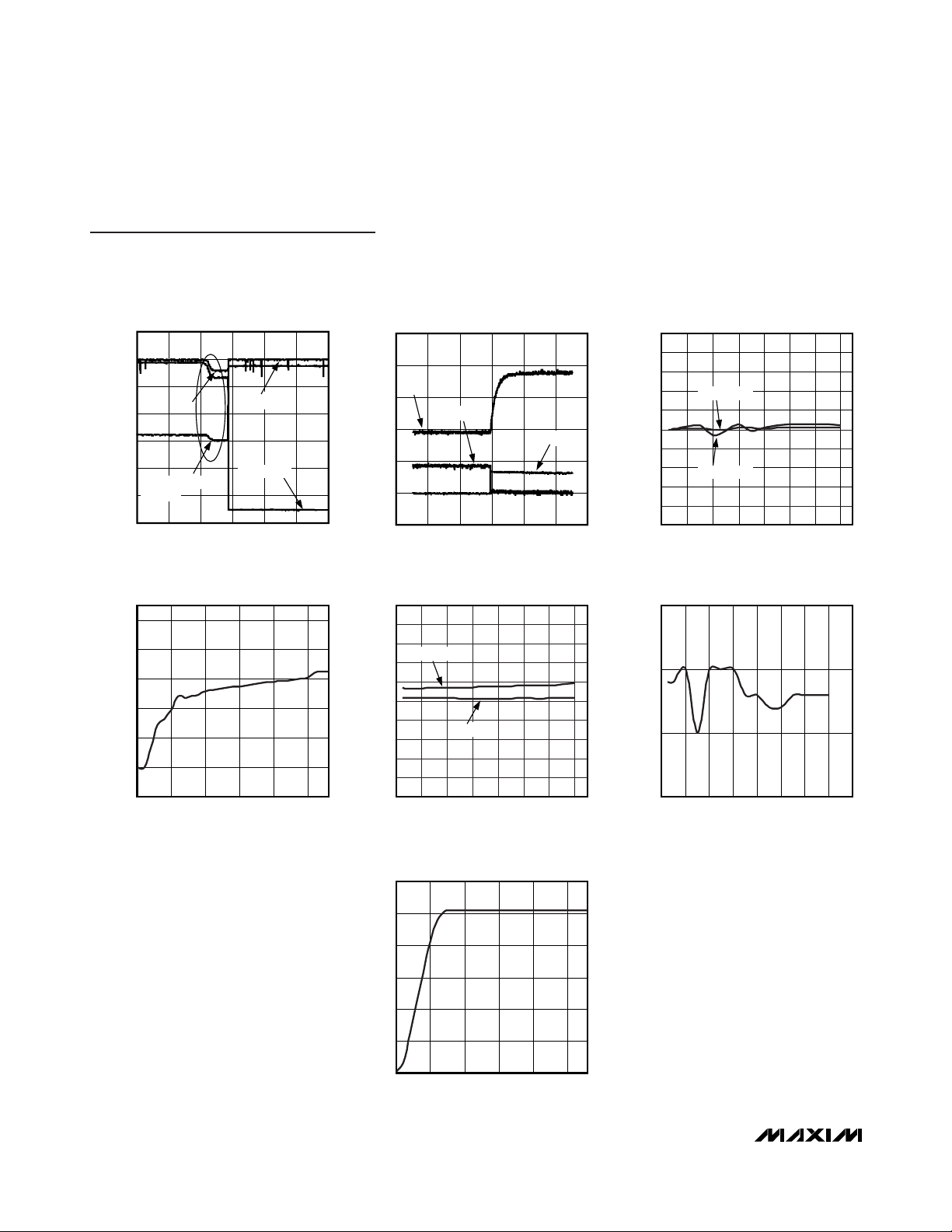
Typical Operating Characteristics
(V
OVLO
= 22.2V and V
UVLO
= 10.1V, R1 = 887kΩ, R2 = 66.5kΩ, R3 = 54.9kΩ, all resistors 1%, OV
REF
= UV
REF
= 1.228V.)
GATE1 Leakage Current G1I
GATE2 Leakage Current G2I
PARAMETER SYMBOL CONDITIONS MIN TYP MAX UNITS
LKGV OV S
LKGVCB
> OV
= 0V -1 +1 µA
CB
Logic-Level High V
Logic-Level Low V
CB Pulldown Resistor R
IH
IL
CBPD
TIMING
V
> VIN > V
Debounce Time t
GATE1 Assertion Delay from
CB Pin
GATE2 Assertion Delay from
CB Pin
Blanking Time t
DEB
t1
GATE
t2
GATE
BLANK
OVP
GATE1 to go low
CB = +3V to 0
rise time = fall time = 5ns (Note 3)
CB = 0 to +3V
rise time = fall time = 5ns (Note 3)
MAX4960
SOURCE1/GATE1 Resistance R
GATE1/Ground Resistance R
SG
GG
(MAX4960) 140 200 260 kΩ
GATE1 Asserted (MAX4960) 140 200 260 kΩ
, V
R E F
U V S
< U V
R E F
, or V
= + 5V -1 +1 µA
C B
1.5 V
123MΩ
for greater than t
UVP
DEB
for
10 25 40 ms
10 25 40 ms
0.4 V
50 ns
50 ns
POWER-UP RESPONSE
(R
V
V
GATE1
V
DD
PULLUP
IN
TIME (μs)
12
10
8
6
4
VOLTAGE (V)
2
0
-2
-150 150
= 1kΩ)
OVERVOLTAGE RESPONSE
30
V
V
IN
GATE1
MAX4959/60 toc01
100500-50-100
25
20
15
VOLTAGE (V)
10
5
0
-150 150
(R
PULLUP
TIME (μs)
= 5kΩ)
MAX4959/60 toc02
V
DD
100500-50-100
UNDERVOLTAGE RESPONSE
(WITHIN BLANKING TIME)
= 1kΩ)
(R
16
14
12
V
IN
10
8
VOLTAGE (V)
6
V
GATE1
4
2
0
070
PULLUP
DRAIN OF P1
MAX4959/60 toc03
605010 20 30 40
TIME (μs)
Page 4
MAX4959/MAX4960
High-Voltage OVP with Battery Switchover
4 _______________________________________________________________________________________
)
Typical Operating Characteristics (continued)
(V
OVLO
= 22.2V and V
UVLO
= 10.1V, R1 = 887kΩ, R2 = 66.5kΩ, R3 = 54.9kΩ, all resistors 1%, OV
REF
= UV
REF
= 1.228V.)
LOW-POWER ADAPTER RESPONSE
= 22.3V, V
(V
OVLO
13
11
9
7
5
VOLTAGE (V)
3
LOAD BECOMES
PRESENT
1
-1
0 0.3
= 10.1V, pFET = IRF7726
UVLO
V
IN
V
DRAIN OF P1
TIME (s)
MAX4959/60 toc04
GATE1
VOLTAGE (V)
0.250.20.150.1.05
SUPPLY CURRENT vs. INPUT VOLTAGE
200
MAX4959/60 toc07
LOGIC THRESHOLD (V)
252015105
(μA)
SUPP
I
160
120
-40
80
40
0
0
VIN (V)
BATTERY SWITCHOVER WITH ADAPTER-
PLUGGED RESPONSE
= 19V, V
(V
IN
25
20
15
10
5
0
-5
GATE2-PULLUP
V
GATE1
V
-150 150
GATE2
= 4.2V, R
TIME (μs)
PULLUP
CB
100500-50-100
LOGIC-INPUT THRESHOLD vs. TEMPERATURE
2
1.8
1.6
1.4
1.2
0.8
0.6
0.4
0.2
V
TH-HI
1
V
TH-LO
0
-50
TEMPERATURE (°C)
= 5kΩ)
907030 50-10 10-30
MAX4959/60 toc05
MAX4959/60 toc08
OVERVOLTAGE AND UNDERVOLTAGE TRIP
DIFFERENCE vs. TEMPERATURE
= 1kΩ)
(R
5
4
3
2
1
0
VOLTAGE (V)
-1
-2
-3
-4
-5
-50 90
PULLUP
UV TRIP DIFF
OV TRIP DIFF
TEMPERATURE (°C)
VDD SUPPLY CURRENT vs. TEMPERATURE
5
4.5
4
SUPPLY CURRENT (μA)
DD
V
3.5
-50 110
TEMPERATURE (°C)
MAX4959/60 toc06
70503010-10-30
MAX4959/60 toc09
9070503010-10-30
VOLTAGE RANGE vs. INPUT VOLTAGE RANGE
6
5
4
(V)
3
DD
V
2
1
0
0
1052515 20
VIN (V)
MAX4959/60 toc10
Page 5
Detailed Description
The MAX4959/MAX4960 provide up to +28V overvoltage
protection for low-voltage systems. When the input voltage exceeds the overvoltage trip level, the MAX4959/
MAX4960 turn off an external pFET to prevent damage
to the protected components.
The MAX4959/MAX4960 feature a control bit (CB) pin
that controls an external battery-switchover function that
switches in the battery when the adapter is unconnected. The host system detects when the battery switchover
must take place and pulls CB high to turn on P2. The
load current is not interrupted during battery switchover
as the body diode of P2 conducts until the CB line is driven high (see the
MAX4959 Typical Operating Circuit 1
,
Figure 4).
An additional safety feature latches off pFET P1 when a
low-power adapter is plugged in. This protects the system from seeing repeated adapter insertions and
removals when an incorrect low-power adapter is
plugged in that cannot provide sufficient current.
Undervoltage Lockout (UVLO)
The MAX4959/MAX4960 have an adjustable undervoltage lockout threshold ranging from +5V to +28V. When
VINis less than the V
UVLO
, the device waits for a blank-
ing time, t
BLANK
, to see if the fault still exists. If the fault
does not exist at the end of t
BLANK
, P1 remains on. If
VINis less than V
UVLO
for longer than the blanking
time, the device turns P1 off and P1 does not turn on
again until VIN< 0.75V. See Figure 1.
Overvoltage Lockout (OVLO)
The MAX4959/MAX4960 have an adjustable overvoltage lockout threshold ranging from +6V to +28V. When
VINis greater than the V
OVLO
, the device turns P1 off
immediately. When V
IN
drops below V
OVLO,
P1 turns on
again after the debounce time has elapsed.
Device Operation
High-Voltage Adapter (V
IN
> V
OVLO
)
If an adapter with a voltage higher than V
OVLO
is
plugged in, the MAX4959/MAX4960 is in an OVP condition, so P1 is kept off or immediately turned off. There is
MAX4959/MAX4960
High-Voltage OVP with Battery Switchover
_______________________________________________________________________________________ 5
Pin Description
PIN
MAX4959
NAME FUNCTION
1 1 GATE1
pFET Gate Drive Output Open Drain. GATE1 is actively driven low, except during fault
(OVP or UVP) condition (the external PFET is turned off). When V
UVLO
< VIN < V
OVLO
,
GATE1 is driven low (the external PFETP1 is turned on).
2, 9 9 N.C. No Connection. Not internally connected. (Connect to ground or leave unconnected.)
—2
pFET Source Output. An internal resistor is connected between SOURCE1 and GATE1.
33IN
Voltage Input. IN is both the power-supply input and the overvoltage/undervoltage
sense input. Bypass IN to GND with a 1µF ceramic capacitor to get a ±15kV protected
input. A minimum 0.1µF ceramic capacitor is required for proper operation.
4 4 UVS
Undervoltage Threshold Set Input. Connect UVS to an external resistive divider from IN to
GND to set the undervoltage lockout threshold. (See Typical Operating Circuits.)
5 5 OVS
Overvoltage Threshold Set Input. Connect OVS to an external resistive divider from
IN to GND to set the overvoltage lockout threshold. (See Typical Operating Circuits.)
66V
DD
Inter nal P ow er - S up p l y Outp ut. Byp ass V D D to GN D w i th a 0.1µF m i ni m um cap aci tor .
V D D p ow er s the i nter nal p ow er - on r eset ci r cui ts. ( S ee the V
D D
C ap aci tor S el ecti on secti on.)
77CB
Battery Switchover Control Input. When CB is high, GATE1 is high (P1 is off), and GATE2
is low (P2 is on). When CB is low, GATE1 is controlled by internal logic and GATE2 is
high (P2 is off). GATE1 is controlled by CB only if V
ULO
< VIN < V
OVLO
.
8 8 GND Ground
10 10 GATE2
pFET Gate Drive Output, Open Drain. When CB is high, GATE2 is low (P2 is on).
When CB is low, GATE2 is high impedance (P2 is off).
MAX4960
SOURCE1
Page 6
MAX4959/MAX4960
no blanking time for OVP, but the debounce time
applies once the IN voltage falls below V
OVLO
but
above V
UVLO
. When the voltage at IN is higher than
V
OVLO
, the CB pin does not control P1.
Correct Adapter (V
UVLO
< VIN< V
OVLO
)
In this case, when the adapter is plugged in, the device
goes through a 20ms (typ) debounce time and ensures
that the voltage at IN is between V
UVLO
and V
OVLO
before P1 is turned on. In this state, the CB pin controls
both P1 and P2.
Low-Power Adapter or Glitch Condition
If the adapter has the correct voltage but not enough
power (incorrect low-power adapter), the MAX4959/
MAX4960 protect pFET P1 from oscillation. When the
adapter is first plugged in, P1 is off so the voltage is correct. When P1 is turned on after the debounce time, the
low-power adapter is dragged down to below V
UVLO
.
The device waits for a 10ms blanking time to make sure
it is not a temporary glitch, and, if a fault still exists, it
latches off P1. P1 does not turn on again until the
adapter is unplugged (VIN<~0.75V) and plugged in
again. This feature can work without the battery present
High-Voltage OVP with Battery Switchover
6 _______________________________________________________________________________________
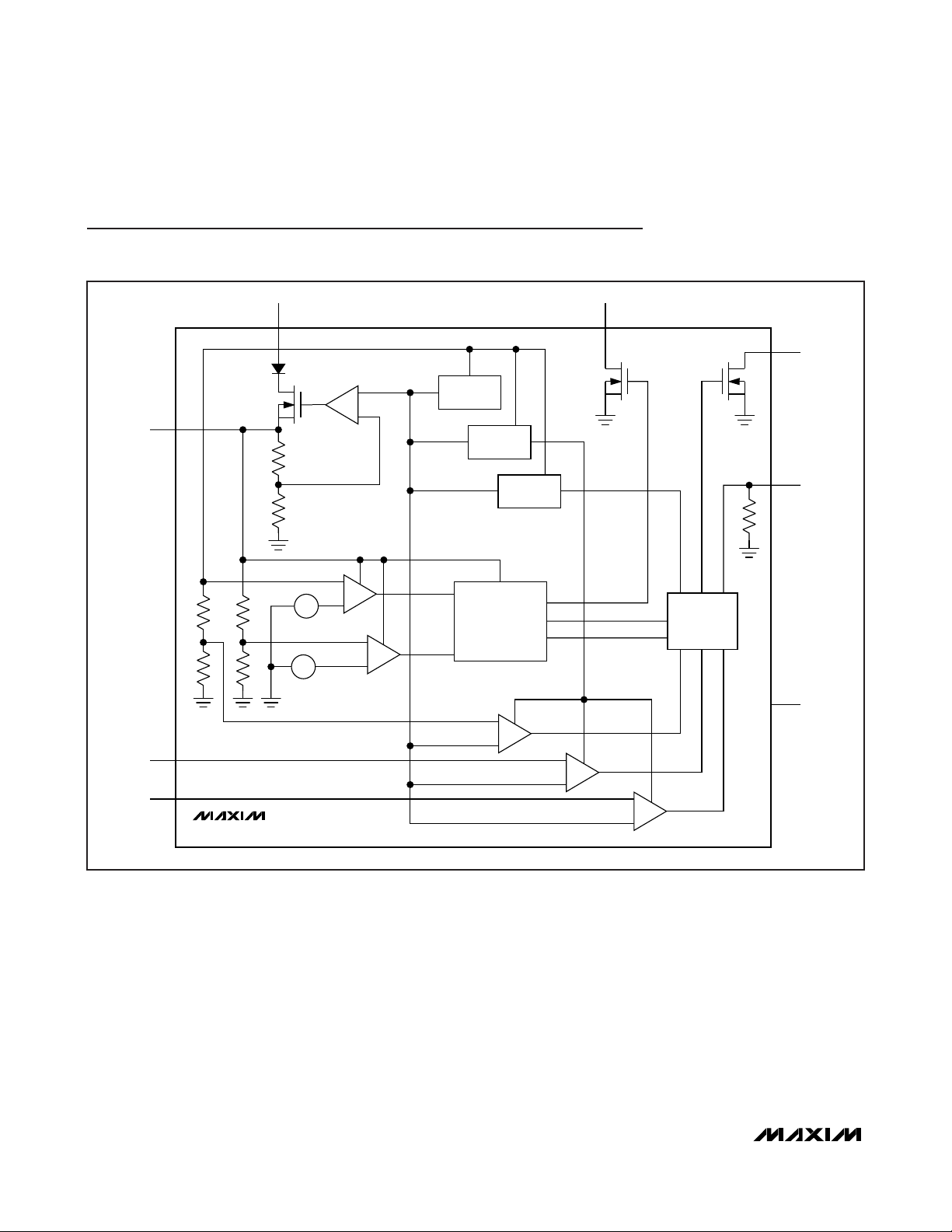
Functional Diagram for the MAX4959
Functional Diagrams
IN
N
V
DD
+
-
+
-
VREF2 = 0.7V
VREF1 = 2V
OVS
UVS
MAX4959
GATE1
GATE2
V
SG
+
-
POWER
ON
V
DD
UVLO
BANDGAP
OFF STORAGE
ANALOG
SUPPLY
POWER-ON
RESET AND
+
-
DIGITAL
SUPPLY
LOGIC
UVLOINT
+
OVLO
+
UVLO
-
N2N1
CB
GND
Page 7

only if the backup capacitor on VDDis large enough to
maintain power for greater than the 10ms blanking time.
The detection that the adapter is unplugged and
plugged in again is implemented by monitoring the V
IN
signal. The adapter is unplugged when VINdrops below
VIN=~ 0.75V, and it is plugged in when VINbecomes
greater than VIN=~ 0.75V. To ensure the monitoring of
this lower threshold, an external storage capacitor at the
VDDpin is necessary. When the input voltage VINdrops
below 4V, power for some internal VINmonitoring circuitry is supplied by the external capacitor at the VDDpin.
This capacitor is supplied by VINthrough a diode and is
internally limited to 5.5V.
Adapter Not Present (VIN< V
UVLO
)
When the input voltage VINdrops below 4.4V, P1 is
turned off automatically and P1 does not turn on again
until the adapter is unplugged (VIN<~0.75V) and
plugged in again. When the adapter is not present, P1 is
kept off with the gate-source resistor (which is internal for
the MAX4960 and external for the MAX4959), and the
CB pin controls the battery switchover pFET P2.
MAX4959/MAX4960
High-Voltage OVP with Battery Switchover
_______________________________________________________________________________________ 7
Functional Diagram for the MAX4960
Functional Diagrams (continued)
IN
V
SG
N
V
DD
VREF2 = 0.7V
+
-
+
-
+
-
POWER
ON
V
DD
UVLO
BANDGAP
OFF STORAGE
ANALOG
SUPPLY
POWER-ON
RESET AND
DIGITAL
SUPPLY
GATE1SOURCE1
GATE2
N2
N1
CB
LOGIC
VREF1 = 2V
OVS
UVS
MAX4960
GND
+
-
UVLOINT
+
OVLO
+
UVLO
-
Page 8

MAX4959/MAX4960
High-Voltage OVP with Battery Switchover
8 _______________________________________________________________________________________
Figure 1. Timing Diagram
The following table lists the different modes of operations:
V
IN
V
OVLO
V
OVLO
V
UVLO
INTUV
V
UVLO
REF
t
V
V
GATE1
DD
DEB
V
CB
V
GATE2
V
DD REGULATED
t
DEB
t
BLANK
t
t
BLANK
DEB
IN RANGE P1 STATE P2 STATE
VIN > V
OVLO
V
< VIN < V
UVLO
OVLO
(debounce timeout ongoing)
V
< VIN < V
UVLO
OVLO
(debounce timeout elapsed)
V
INTUVREF
< VIN < V
OVLO
(blanking timeout ongoing)
V
INTUVREF
< VIN < V
OVLO
(blanking timeout elapsed)
VIN < V
INTUVREF
P1 OFF (not affected by CB)
P1 OFF (not affected by CB)
CB = 1 -> P1 is OFF
CB = 0 -> P1 is ON
CB = 1 -> P1 is OFF
CB = 0 -> P1 is ON
P1 OFF (not affected by CB). P1 does not turn on again until
adapter is unplugged (VIN <~0.75V) and plugged in again.
P1 OFF (not affected by CB). P1 does not turn on again until
adapter is unplugged (V
<~0.75V) and plugged in again.
IN
CB = 1 -> P2 is ON
CB = 0 -> P2 is OFF
Page 9

Applications Information
MOSFET Configuration and Selection
The MAX4959/MAX4960 are used with a single MOSFET configuration as shown in the
Typical Operating
Circuits
to regulate voltage as a low-cost solution.
The MAX4959/MAX4960 are designed with pFETs. For
lower on-resistance, the external MOSFET can be multiple pFETs in parallel. In most situations, MOSFETs with
R
DS(ON)
specified for a VGSof 4.5V work well. Also,
MOSFETs (with VDS≥ 30V) withstand the full +28V IN
range of the MAX4959/MAX4960.
Resistor Selection for
Overvoltage/Undervoltage Window
The MAX4959/MAX4960 include undervoltage and
overvoltage comparators for window detection (see
Figure 4). GATE1 is enhanced and after the debounce
time, the pFET is turned on when the monitored voltage
is within the selected window.
The resistor values R1, R2, and R3 can be calculated
as follows:
where R
TOTAL
= R1 + R2 + R3.
Use the following steps to determine the values for R1,
R2, and R3:
1) Choose a value for R
TOTAL
, the sum of R1, R2, and
R3. Because the MAX4959/4960 have very high
input impedance, R
TOTAL
can be up to 5MΩ.
2) Calculate R3 based on R
TOTAL
and the desired
V
OVLO
trip point:
3) Calculate R2 based on R
TOTAL
, R3, and the desired
V
UVLO
trip point:
4) Calculate R1 based on R
TOTAL
, R2, and R3:
R1 = R
TOTAL
– R2 – R3
Note that the ratio between the externally set OVLO and
UVLO threshold must not exceed:
4 [V
OVLO
/ V
UVLO]MAX
≤ 4)
VDDCapacitor Selection
VDDis regulated to +5V by a linear regulator. Since the
minimum external adjustable UVLO trip threshold is
+5V, the VDDrange is +5V to +28V and the value at
VDDis:
VDD= VIN– 0.8V where VIN= 5V to 5.8V
VDD= +5V where VIN> 5.8V
The capacitor at VDDmust be large enough to provide
power to the device for an external settable time,
t
HOLD
, when VINdrops to 0V. The capacitor value to
have a minimum time of t
HOLD
is:
C = (I
VDD
x t
HOLD
) / (VDD- VDDUVLO)
The worst case scenario is where VIN= +5V, VDD= V
IN
- 0.8V = +4.2V, I
VDD
= 10µA (max). For a t
HOLD
time of
20ms, C = (10µA x 20ms) / (4.2V - 2.2V) = 100nF.
Note: The capacitor must be greater than 100nF for the
internal regulator to be stable, and needs to have low
ESR and low leakage current, for example, a ceramic
capacitor.
IN Bypass Considerations
For most applications, bypass IN to GND with a 1µF
ceramic capacitor. If the power source has significant
inductance due to long lead length, take care to prevent overshoots due to the LC tank circuit, and provide
protection if necessary to prevent exceeding the +30V
absolute maximum rating on VIN.
The MAX4959/MAX4960 provide protection against voltage faults up to+28V, but this does not include negative
voltages. If negative voltages are a concern, connect a
Schottky diode from IN to GND to clamp negative input
voltages.
ESD Test Conditions
The MAX4959/MAX4960 are protected from ±15kV
Human Body Model ESD on IN when IN is bypassed to
ground with a 1µF ceramic capacitor.
Human Body Model
Figure 2 shows the Human Body Model and Figure 3
shows the current waveform it generates when discharged into a low impedance. This model consists of a
100pF capacitor charged to the ESD voltage of interest
that is then discharged into the device through a 1.5kΩ
resistor.
MAX4959/MAX4960
High-Voltage OVP with Battery Switchover
_______________________________________________________________________________________ 9
VU
UVLO REF
VO
OVLO REF
R
R
3 =
23=
V
=
()
=
V
()
OR
⎡
⎢
⎣
×V
REF TOTAL
V
OVLO
UR
×
V
REF TOTAL
V
UVLO
⎛
R
⎜
R
⎝
R
⎛
⎜
⎝
⎞
TOTAL
⎟
R
23
+
⎠
⎞
TOTAL
⎟
⎠
R
3
⎤
−
R
⎥
⎦
Page 10

MAX4959/MAX4960
Chip Information
PROCESS: BiCMOS
High-Voltage OVP with Battery Switchover
10 ______________________________________________________________________________________
Figure 2. Human Body ESD Test Model
IP 100%
90%
36.8%
t
RL
TIME
t
DL
CURRENT WAVEFORM
PEAK-TO-PEAK RINGING
(NOT DRAWN TO SCALE)
I
r
10%
0
0
AMPERES
Figure 3. Human Body Current Waveform
R
D
1.5kΩ
DISCHARGE
RESISTANCE
STORAGE
CAPACITOR
HIGH-
VOLTAGE
DC
SOURCE
R
C
1MΩ
CHARGE-CURRENT-
LIMIT RESISTOR
C
s
100pF
DEVICE
UNDER
TEST
Page 11

MAX4959/MAX4960
High-Voltage OVP with Battery Switchover
______________________________________________________________________________________ 11
Typical Operating Circuits
Figure 4. MAX4959 Typical Operating Circuit 1
AC ADAPTER
D1
N1
UVLO
GATE1IN
RD1
P1
OVLO
LOGIC
C2
RD2
GATE2
N2
CB
GND
RU2
P2
C1
RU1
V
SUPPLY
HOLD-UP
V
DD
R1
UVS
R2
OVS
R3
POWER SUPPLY
V
REF
DC-DC
CONVERTER
BATTERY
CHARGER
1-CELL (4.2V) TO
4-CELL (16.8V)
Page 12

MAX4959/MAX4960
High-Voltage OVP with Battery Switchover
12 ______________________________________________________________________________________
Typical Operating Circuits (continued)
Figure 5. MAX4959 Typical Operating Circuit 2
28V
AC ADAPTER
PROTECTED
CHARGER
EN
DC-DC
CONVERTER
V
SUPPLY
V
DD
R1
UVS
R2
OVS
R3
HOLD-UP
POWER SUPPLY
RD1
GATE1IN
N1
V
REF
UVLO
OVLO
3.3V
LOGIC
SYSTEM LOAD
GATE2
N2
CB
GND
1-CELL (4.2V) TO
4-CELL (16.8V)
Page 13

MAX4959/MAX4960
High-Voltage OVP with Battery Switchover
______________________________________________________________________________________ 13
Typical Operating Circuits (continued)
Figure 6. MAX4960 Typical Operating Circuit 1
AC ADAPTER
DC-DC
CONVERTER
BATTERY
CHARGER
1-CELL (4.2V) TO
4-CELL (16.8V)
N1
UVLO
P1
C2
GATE1SOURCE1IN
LOGIC
OVLO
RD2
GATE2
N2
CB
GND
RU2
P2
C1
V
SUPPLY
HOLD-UP
V
DD
R1
UVS
R2
OVS
R3
POWER SUPPLY
V
REF
Page 14

MAX4959/MAX4960
High-Voltage OVP with Battery Switchover
14 ______________________________________________________________________________________
Typical Operating Circuits (continued)
Figure 7. MAX4960 Typical Operating Circuit 2
AC ADAPTER
V
SUPPLY
V
DD
R1
UVS
R2
OVS
R3
HOLD-UP
POWER SUPPLY
BATTERY
LOGIC
CHARGER
DC-DC
CONVERTER
SYSTEM LOAD
GATE2
N2
CB
GND
1-CELL (4.2V) TO
4-CELL (16.8V)
C1
SOURCE1
V
REF
P1
GATE1IN
N1
UVLO
OVLO
Page 15

MAX4959/MAX4960
High-Voltage OVP with Battery Switchover
______________________________________________________________________________________ 15
Package Information
(The package drawing(s) in this data sheet may not reflect the most current specifications. For the latest package outline information,
go to www.maxim-ic.com/packages
.)
D
XXXX
XXXX
XXXX
PIN 1
INDEX AREA
SAMPLE
MARKING
7
A1
A
E
L
b
A
A2
L
e
C
L
e
EVEN TERMINAL
A A
(N/2 -1) x e)
b
N
1
C
L
e
ODD TERMINAL
SOLDER
MASK
COVERAGE
PIN 1
0.10x45∞
L1
L
6, 8, 10L UDFN.EPS
-DRAWING NOT TO SCALE-
PACKAGE OUTLINE,
6, 8, 10L uDFN, 2x2x0.80 mm
21-0164
1
A
2
Page 16

MAX4959/MAX4960
High-Voltage OVP with Battery Switchover
16 ______________________________________________________________________________________
Package Information (continued)
(The package drawing(s) in this data sheet may not reflect the most current specifications. For the latest package outline information,
go to www.maxim-ic.com/packages
.)
COMMON DIMENSIONS
SYMBOL MIN. NOM.
A
A1
A2
D 1.95 2.00
E
L
L1
0.70 0.75
0.15 0.20 0.25
0.020 0.025 0.035
1.95 2.00
0.30 0.40
0.10 REF.
MAX.
0.80
2.05
-
2.05
0.50
-DRAWING NOT TO SCALE-
PACKAGE VARIATIONS
PKG. CODE N e b
6L622-1 0.65 BSC 0.30±0.05
0.25±0.050.50 BSC8L822-1
0.20±0.030.40 BSC10L1022-1
(N/2 -1) x e
1.30 REF.
1.50 REF.
1.60 REF.
PACKAGE OUTLINE,
6, 8, 10L uDFN, 2x2x0.80 mm
21-0164
2
A
2
Page 17

MAX4959/MAX4960
High-Voltage OVP with Battery Switchover
Maxim cannot assume responsibility for use of any circuitry other than circuitry entirely embodied in a Maxim product. No circuit patent licenses are
implied. Maxim reserves the right to change the circuitry and specifications without notice at any time.
Maxim Integrated Products, 120 San Gabriel Drive, Sunnyvale, CA 94086 408-737-7600 ____________________
17
© 2007 Maxim Integrated Products is a registered trademark of Maxim Integrated Products, Inc.
SPRINGER
Package Information (continued)
(The package drawing(s) in this data sheet may not reflect the most current specifications. For the latest package outline information,
go to www.maxim-ic.com/packages
.)
e
10
Ø0.50±0.1
0.6±0.1
1
0.6±0.1
TOP VIEW
D2
A2
D1
FRONT VIEW
4X S
10
DIM
H
1
BOTTOM VIEW
E2
GAGE PLANE
A
b
A1
α
E1
L
L1
SIDE VIEW
INCHES
MIN
-A
0.002
A1
A2 0.030 0.037 0.75 0.95
0.116
D1
0.114
D2
0.116
E1
0.114
E2
0.187
H
0.0157
L
L1
0.037 REF
0.007
b
e
0.0197 BSC
0.0035
c
0.0196 REF
S
α
0° 0° 6°
c
MAX
0.043
0.006
0.120
0.118
0.120
0.118
0.199
0.0275
0.0106
0.0078
6°
MILLIMETERS
MAX
MIN
-
1.10
0.05
0.15
2.95
3.05
2.89
3.00
2.95
3.05
2.89
3.00
4.75
5.05
0.40
0.70
0.940 REF
0.177
0.270
0.500 BSC
0.090
0.200
0.498 REF
10LUMAX.EPS
PROPRIETARY INFORMATION
TITLE:
PACKAGE OUTLINE, 10L uMAX/uSOP
REV.DOCUMENT CONTROL NO.APPROVAL
21-0061
1
1
 Loading...