

Page 1
General Description
The MAX4850/MAX4850H/MAX4852/MAX4852H family
of dual SPDT (single-pole/double-throw) switches operate from a single +2V to +5.5V supply and can handle
signals greater than the supply rail. These switches feature low 3.5Ω or 3.5Ω/7Ω on-resistance with low oncapacitance, making them ideal for switching audio
and data signals.
The MAX4850/MAX4850H are configured with two
SPDT switches and feature two comparators for headphone detection or mute/send key functions. The
MAX4852 has two SPDT switches with no comparators
for low 1µA supply current.
For over-rail applications, these devices offer either the
pass-through or high-impedance option. For the
MAX4850/MAX4852, the signal (up to 5.5V) passes
through the switch without distortion even when the positive supply rail is exceeded. For the MAX4850H/
MAX4852H, the switch input becomes high impedance
when the input signal exceeds the supply rail.
The MAX4850/MAX4850H/MAX4852/MAX4852H are
available in the space-saving (3mm x 3mm), 16-pin
TQFN package and operate over the extended temperature range of -40°C to +85°C.
Applications
USB Switching
Audio-Signal Routing
Cellular Phones
Notebook Computers
PDAs and Other Handheld Devices
Features
♦ USB 2.0 Full Speed (12MB) and USB 1.1 Signal
Switching Compliant
♦ Switch Signals Greater than V
CC
♦ 0.1ns Differential Skew
♦ 3.5Ω/7Ω On-Resistance
♦ 135MHz -3dB Bandwidth
♦ +2V to +5.5V Supply Range
♦ 1.8V Logic Compatible
♦ Low Supply Current
1µA (MAX4852)
5µA (MAX4850)
10µA (MAX4850H/MAX4852H)
♦ Available in a Space-Saving (3mm x 3mm),
16-Pin TQFN Package
MAX4850/MAX4850H/MAX4852/MAX4852H
Dual SPDT Analog Switches with
Over-Rail Signal Handling
________________________________________________________________ Maxim Integrated Products 1
Ordering Information
V
CC
3
MAX4850
MAX4850H
NC1
NO1
NC2
NO2
COUT2
COM1
IN1
IN2
COM2
CIN2
V
CC
3
COUT1
CIN1
MAX4852
MAX4852H
NC1
NO1
NC2
NO2
COM1
IN1
IN2
COM2
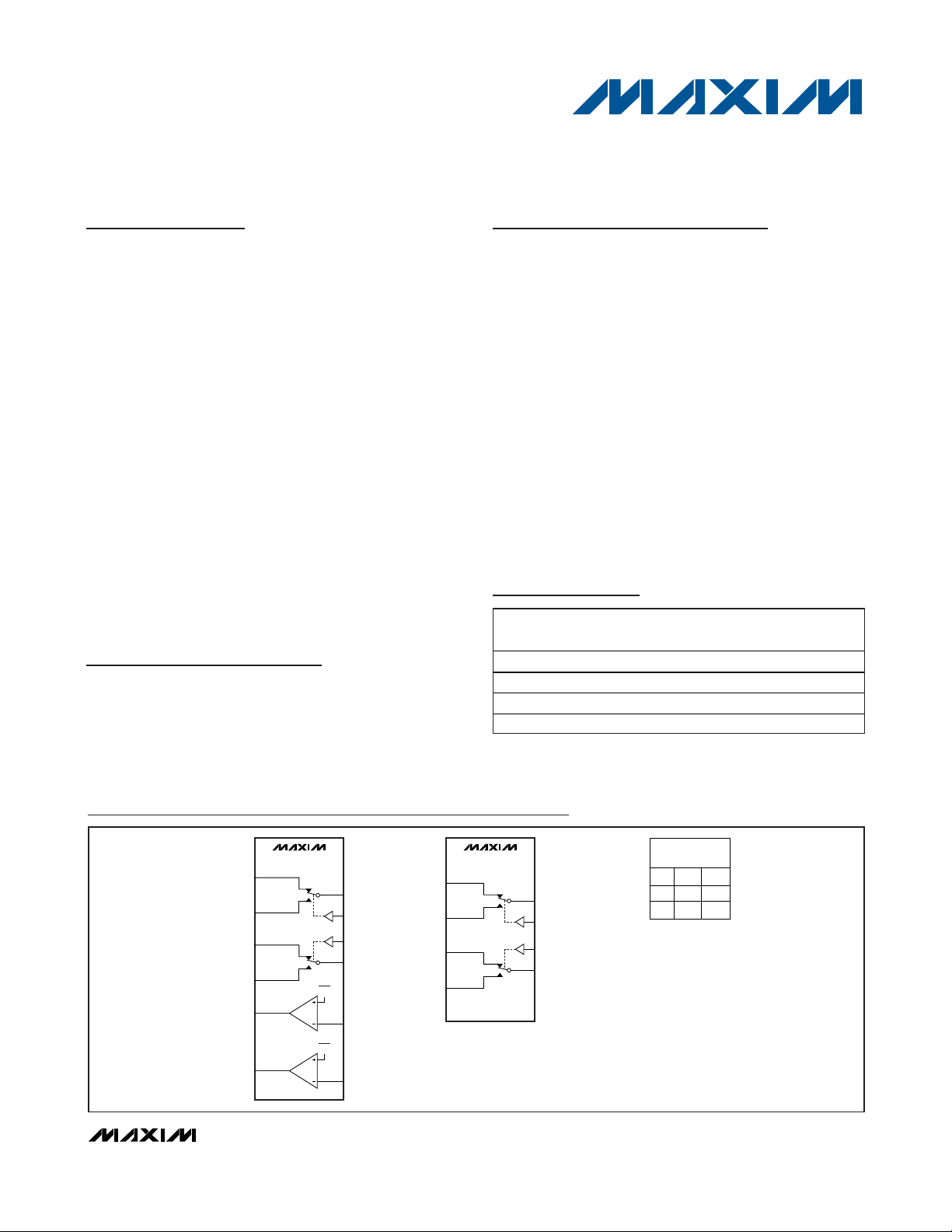
MAX4850_
MAX4852_
IN_ NO_ NC_
0 OFF ON
1 ON OFF
SWITCHES SHOWN FOR
LOGIC 0 INPUT
3.5Ω
3.5Ω
7Ω
3.5Ω
3.5Ω
7Ω
Block Diagrams/Truth Table
19-3375; Rev 0; 7/04
For pricing, delivery, and ordering information, please contact Maxim Direct at 1-888-629-4642,
or visit Maxim’s website at www.maxim-ic.com.
*EP = Exposed paddle.
Pin Configurations and Selector Guide appear at end of
data sheet.
PART TEMP RANGE PIN-PACKAGE
MAX4850ETE -40°C to +85°C 16 TQFN-EP* ABU
MAX4850HETE -40°C to +85°C 16 TQFN-EP* ABV
MAX4852ETE -40°C to +85°C 16 TQFN-EP* ABZ
MAX4852HETE -40°C to +85°C 16 TQFN-EP* ACA
TOP
MARK
Page 2
Dual SPDT Analog Switches with
Over-Rail Signal Handling
2 _______________________________________________________________________________________
ABSOLUTE MAXIMUM RATINGS
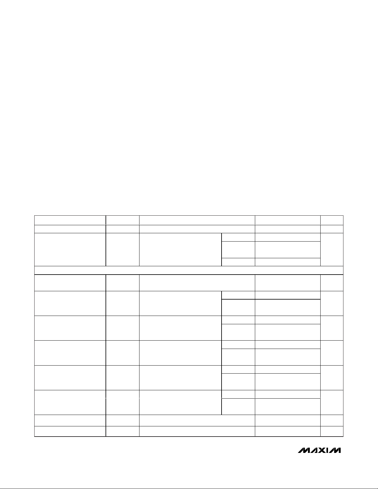
ELECTRICAL CHARACTERISTICS
(VCC= +2.7V to +5.5V, TA= -40°C to +85°C, unless otherwise noted. Typical values are at VCC= +3.0V, TA= +25°C, unless otherwise noted.) (Note 2)
Stresses beyond those listed under “Absolute Maximum Ratings” may cause permanent damage to the device. These are stress ratings only, and functional
operation of the device at these or any other conditions beyond those indicated in the operational sections of the specifications is not implied. Exposure to
absolute maximum rating conditions for extended periods may affect device reliability.
VCC, IN_, CIN_, COM_, NO_,
NC_ to GND (Note 1).........................................-0.3V to +6.0V
COUT_........................................................-0.3V to (V
CC
+ 0.3V)
COUT_ Continuous Current..............................................±20mA
Closed Switch Continuous Current COM_, NO_, NC_
3.5Ω Switch ................................................................±100mA
7Ω Switch .....................................................................±50mA
Peak Current COM_, NO_, NC_ (pulsed at 1ms, 50% duty cycle)
3.5Ω Switch ................................................................±200mA
7Ω Switch ...................................................................±100mA
Peak Current COM_, NO_, NC_ (pulsed at 1ms, 10% duty cycle)
3.5Ω Switch ................................................................±240mA
7Ω Switch ...................................................................±120mA
Continuous Power Dissipation (T
A
= +70°C)
16-Pin TQFN (derate 20.8mW/°C above +70°C) ...........1667mW
Operating Temperature Range ...........................-40°C to +85°C
Junction Temperature......................................................+150°C
Storage Temperature Range .............................-65°C to +150°C
Lead Temperature (soldering, 10s) .................................+300°C
MAX4850/MAX4850H/MAX4852/MAX4852H
Note 1: Signals on IN, NO, NC, or COM below GND are clamped by internal diodes. Limit forward-diode current to maximum
current rating.
PARAMETER SYMBOL CONDITIONS MIN TYP MAX UNITS
Supply Voltage V
Supply Current I
ANALOG SWITCH (3.5Ω Switch)
Analog Signal Range
On-Resistance (Note 3) R
On-Resistance Match
Between Channels
(Notes 3, 4)
On-Resistance Flatness
(Note 5)
NO_/NC_ Off-Leakage
Current
COM_ On-Leakage Current I
-3dB Bandwidth BW Signal = 0dBm, RL = 50Ω, CL = 5pF (Figure 5) 100 MHz
V
NO_
V
CC
CC
, V
COM_
ON
ΔR
R
FLAT
I
OFF
ON
ON
VCC = 5.5V, V
,
NC_
VCC = 3V, I
V
(MAX485_) or V
VCC = 3V, I
V
VCC = 3V, I
V
VCC = 5.5V, V
or 4.5V, V
VCC = 5.5V; V
4.5V, or floating;
V
IN_
COM_
NC_
NC_
NC_
COM_
or V
or V
or V
= 0 to 5.5V
NO_
COM
= 1.5V
NO_
COM_
= 1V, 2V, 3V
NO_
NC_
COM_
NC_
= 1V, 4.5V, or floating
2.0 5.5 V
MAX4850 5 10
= 0V or V
CC
MAX4850H/
MAX4852H
10 20
MAX4852 1
0 5.5 V
= 10mA,
(MAX485_H)
CC
TA = +25°C 3.5 4.5
= -40°C
T
A
to +85°C
TA = +25°C 0.1 0.2
= 10mA,
T
= -40°C
A
to +85°C
TA = +25°C 1.2 1.8
= 10mA,
T
= -40°C
A
to +85°C
TA = +25°C -2 +2
or V
= 4.5V or 1V
or V
NO_
NO_
= 1V
= 1V,
T
= -40°C
A
to +85°C
-10 +10
TA = +25°C -2 +2
T
= -40°C
A
to +85°C
-12.5 +12.5
5
0.25
2
µA
Ω
Ω
Ω
nA
nA
NO_/NC_ Off-Capacitance C
OFF
f = 1MHz (Figure 6) 20 pF
Page 3
MAX4850/MAX4850H/MAX4852/MAX4852H
Dual SPDT Analog Switches with
Over-Rail Signal Handling
_______________________________________________________________________________________ 3
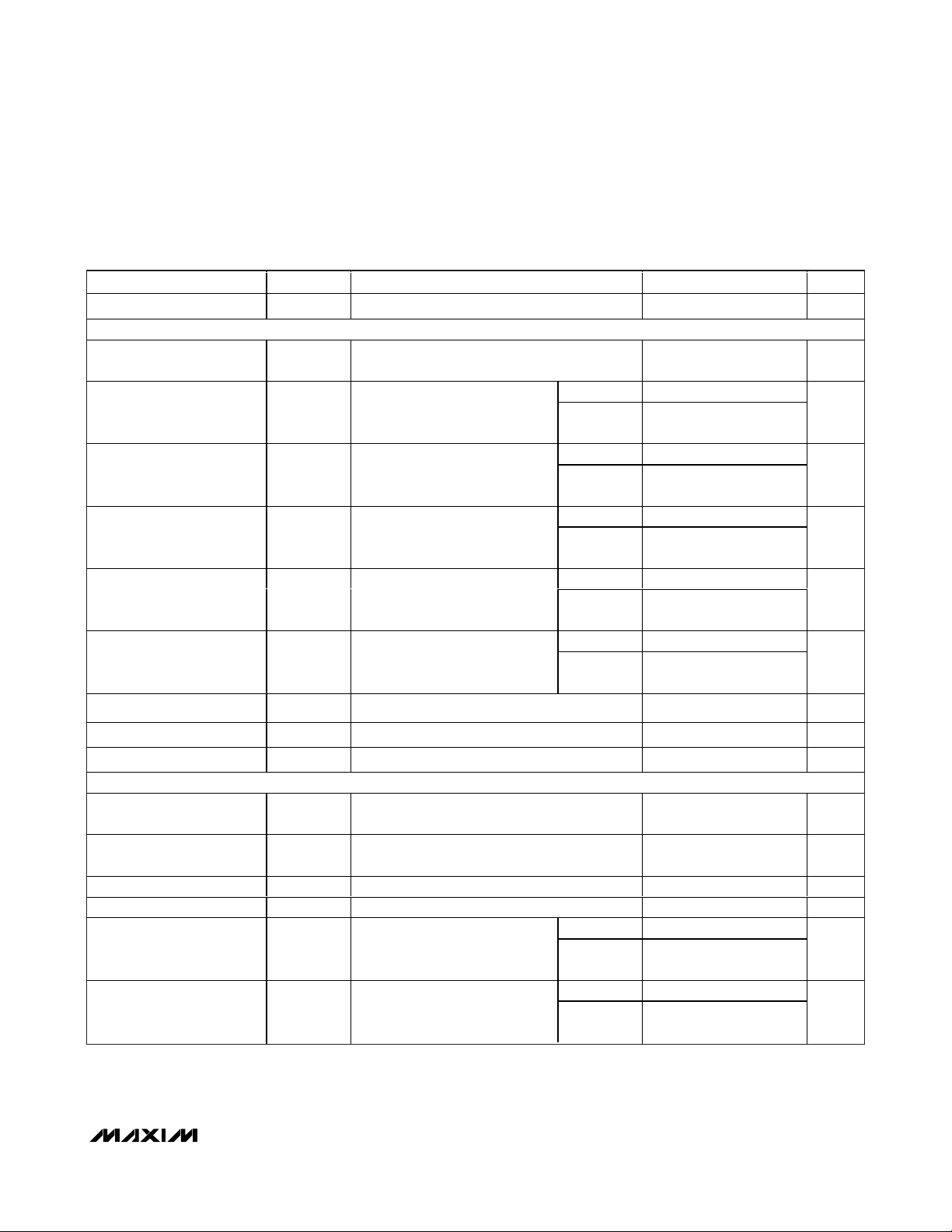
ELECTRICAL CHARACTERISTICS (continued)
(VCC= +2.7V to +5.5V, TA= -40°C to +85°C, unless otherwise noted. Typical values are at VCC= +3.0V, TA= +25°C, unless otherwise noted.) (Note 2)
PARAMETER SYMBOL CONDITIONS MIN TYP MAX UNITS
COM On-Capacitance C
ON
ANALOG SWITCH (7Ω Switch)
V
, V
Analog Signal Range
On-Resistance R
NO_
V
COM_
ON
On-Resistance Match
Between Channels
ΔR
ON
(Notes 3, 4)
On-Resistance Flatness
(Note 5)
NO_/NC_ Off-Leakage
Current
COM_ On-Leakage Current I
R
I
FLAT
OFF
ON
-3dB Bandwidth BW Signal = 0dBm, RL = 50Ω, CL = 5pF (Figure 5) 135 MHz
f = 1MHz (Figure 6) 60 pF
,
NC_
VCC = 3V, I
or V
or V
COM_
= 0 to 5.5V (MAX4852)
NO_
(MAX4852H)
CC
= 10mA, V
TA = +25°C 7 9
NC_
= -40°C
T
A
to +85°C
0 5.5 V
TA = +25°C 0.2 0.4
VCC = 3V, I
= 1.5V
V
NO_
= 10mA, V
COM
NC_
or
T
= -40°C
A
to +85°C
TA = +25°C 2.5 3.75
VCC = 3V, I
or V
= 1V, 2V, 3V
NO_
COM_
= 10mA, V
NC_
T
= -40°C
A
to +85°C
TA = +25°C -2 +2
VCC = 5.5V, V
or 4.5V, V
VCC = 5.5V; V
4.5V, or floating; V
4.5V, or floating
NC_
= 4.5V or 1V
COM_
NC_
or V
or V
COM_
NO_
NO_
= 1V,
= 1V
= 1V,
T
= -40°C
A
to +85°C
-10 +10
TA = +25°C -2 +2
T
= -40°C
A
to +85°C
-12.5 +12.5
10
0.5
4.0
Ω
Ω
Ω
nA
nA
NO_/NC_ Off-Capacitance C
COM On-Capacitance C
DYNAMIC CHARACTERISTICS
Signal Over-Rail to High-Z
Switching Time
High-Z to Low-Z Switching
Time
Skew (Note 3) t
Propagation Delay (Note 3) t
Turn-On Time t
Turn-Off Time t
OFF
ON
t
HIZ
t
HIZB
SKEW
PD
ON
OFF
f = 1MHz (Figure 6) 12 pF
f = 1MHz (Figure 6) 50 pF
MAX4850H/MAX4852H, V
(V
+ 0.5V), VCC < 5V (Figure 1)
CC
MAX4850H/MAX4852H, V
+ 0.5V) to VCC, VCC < 5V (Figure 1)
(V
CC
NO_
NO_
or V
or V
NC_
NC_
= VCC to
=
0.5 1 µs
0.5 1 µs
RS = 39Ω, CL = 50pF (Figure 2) 0.1 1 ns
RS = 39Ω, CL = 50pF (Figure 2) 0.9 2 ns
TA = +25°C 40 60
VCC = 3V, V
= 300Ω, CL = 50pF (Figure 1)
R
L
NO_
or V
NC_
= 1.5V,
T
= -40°C
A
to +85°C
100
ns
TA = +25°C 30 40
VCC = 3V, V
R
= 300Ω, CL = 50pF (Figure 1)
L
NO_
or V
NC_
= 1.5V,
T
= -40°C
A
to +85°C
60
ns
Page 4
MAX4850/MAX4850H/MAX4852/MAX4852H
Dual SPDT Analog Switches with
Over-Rail Signal Handling
4 _______________________________________________________________________________________
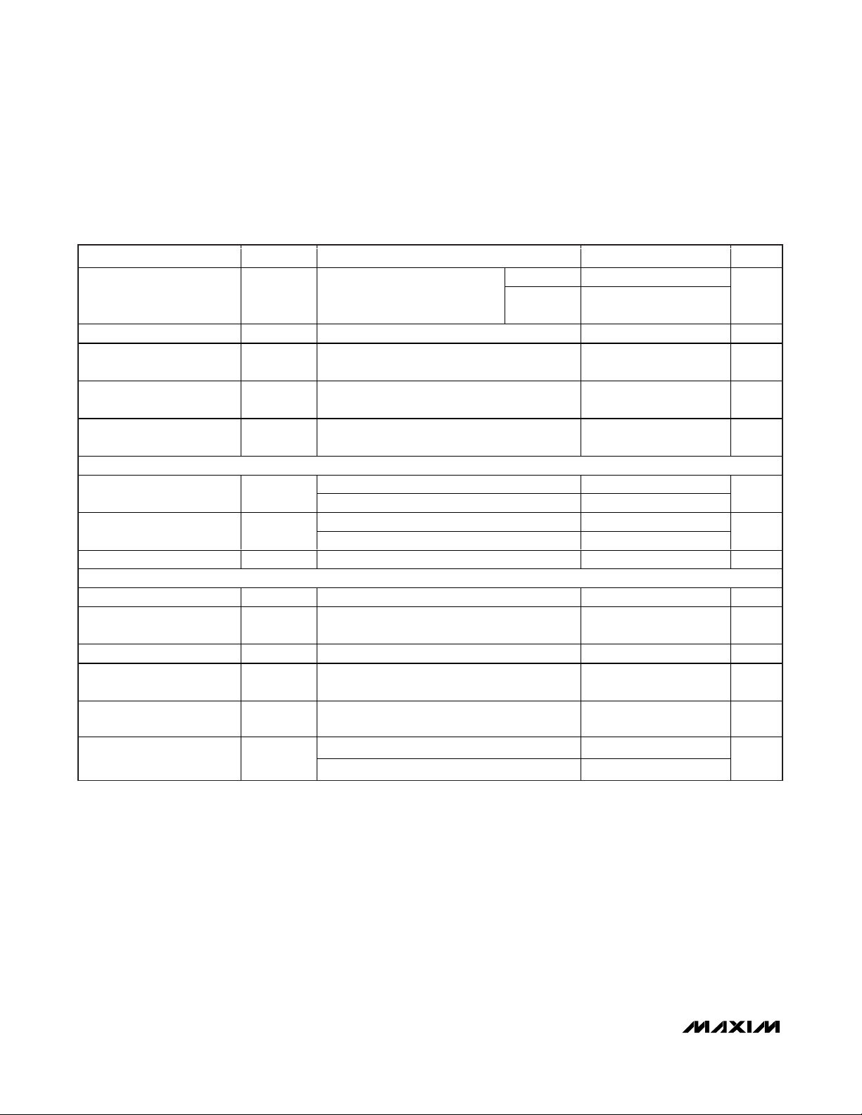
ELECTRICAL CHARACTERISTICS (continued)
(VCC= +2.7V to +5.5V, TA= -40°C to +85°C, unless otherwise noted. Typical values are at VCC= +3.0V, TA= +25°C, unless otherwise noted.) (Note 2)
Note 2: Specifications are 100% tested at TA= +85°C only, and guaranteed by design and characterization over the specified
temperature range.
Note 3: Guaranteed by design and characterization; not production tested.
Note 4: ΔR
ON
= R
ON(MAX)
- R
ON(MIN)
.
Note 5: Flatness is defined as the difference between the maximum and minimum value of on-resistance as measured over the
specified analog signal ranges.
Note 6: Off-isolation = 20log
10(VCOM_
/ V
NO_
), V
COM_
= output, V
NO_
= input to off switch.
PARAMETER SYMBOL CONDITIONS MIN TYP MAX UNITS
Break-Before-Make Time
Delay (Note 3)
t
D
Charge Injection Q V
Off-Isolation (Note 6) V
Crosstalk V
ISO
CT
Total Harmonic Distortion THD
VCC = 3V, V
R
= 300Ω, CL = 50pF (Figure 3)
L
= 1.5V, RS = 0Ω, CL = 1nF (Figure 4) 8 pC
COM_
f = 100kHz, V
C
= 5pF (Figure 5)
L
f = 1MHz, V
NO_
COM_
COM_
or V
= 1V
= 1.5V,
NC_
= 1V
RMS
, RL = 50Ω, CL = 5pF
RMS
(Figure 5)
f = 20Hz to 20kHz, V
R
= 600Ω
L
COM_
= 1V + 2V
DIGITAL I/O (IN_)
Input-Logic High Voltage V
Input-Logic Low Voltage V
Input Leakage Current I
IH
IL
IN
VCC = 2V to 3.6V 1.4
VCC = 3.6V to 5.5V 1.8
VCC = 2V to 3.6V 0.5
VCC = 3.6V to 5.5V 0.8
V
= 0 or 5.5V -0.5 +0.5 µA
IN_
COMPARATOR
Comparator Range 0 5.5 V
Comparator Threshold V
TH
VCC = 2V to 5.5V, falling input
Comparator Hysteresis VCC = 2V to 5.5V 50 mV
Comparator Output High
Voltage
Comparator Output Low
Voltage
Comparator Switching Time
I
I
= 1mA
SOURCE
= 1mA 0.4 V
SINK
Rising input (Figure 7) 2.5
Falling input (Figure 7) 0.5
TA = +25°C 15
T
= -40°C
A
to +85°C
, RL = 50Ω,
,
P-P
2
0.3 x
V
CC
V
CC
0.4V
-80 dB
-95 dB
0.04 %
0.33 x
V
0.36 x
CC
-
ns
V
V
V
CC
V
V
µs
Page 5
MAX4850/MAX4850H/MAX4852/MAX4852H
Dual SPDT Analog Switches with
Over-Rail Signal Handling
_______________________________________________________________________________________ 5
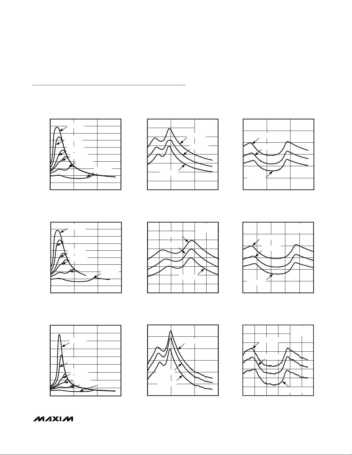
Typical Operating Characteristics
(VCC= 3.0V, TA = +25°C, unless otherwise noted.)
MAX4850/MAX4852
ON-RESISTANCE vs. COM VOLTAGE
10
9
8
7
6
5
4
ON-RESISTANCE (Ω)
3
2
1
0
06
VCC = 1.8V
VCC = 2.0V
VCC = 2.3V
VCC = 2.5V
VCC = 3.0V
COM VOLTAGE (V)
3.5Ω SWITCH
VCC = 5.0V
42
MAX4850 toc01
ON-RESISTANCE (Ω)
MAX4850H/MAX4852H
ON-RESISTANCE vs. COM VOLTAGE
10
9
8
7
6
5
4
ON-RESISTANCE (Ω)
3
2
1
0
06
VCC = 1.8V
VCC = 2.0V
VCC = 2.3V
VCC = 2.5V
VCC = 3.0V
COM VOLTAGE (V)
3.5Ω SWITCH
VCC = 5.0V
42
MAX4850 toc04
ON-RESISTANCE (Ω)
MAX4850/MAX4852
ON-RESISTANCE vs. COM VOLTAGE
4.5
4.0
3.5
3.0
2.5
2.0
1.5
1.0
0.5
TA = -40°C
06
COM VOLTAGE (V)
VCC = 3.0V
3.5Ω SWITCH
TA = +85°C
TA = +25°C
42
MAX4850 toc02
3.5
3.0
2.5
2.0
1.5
ON-RESISTANCE (Ω)
1.0
0.5
06
MAX4850H/MAX4852H
ON-RESISTANCE vs. COM VOLTAGE
5.0
4.5
4.0
3.5
3.0
2.5
2.0
1.5
1.0
0 3.0
TA = +85°C
TA = +25°C
COM VOLTAGE (V)
TA = -40°C
VCC = 3.0V
3.5Ω SWITCH
2.52.00.5 1.0 1.5
MAX4850 toc05
3.5
3.0
2.5
2.0
1.5
ON-RESISTANCE (Ω)
1.0
0.5
05
MAX4850/MAX4852
ON-RESISTANCE vs. COM VOLTAGE
TA = +85°C
TA = +25°C
TA = -40°C
COM VOLTAGE (V)
MAX4850H/MAX4852H
ON-RESISTANCE vs. COM VOLTAGE
TA = +85°C
TA = +25°C
TA = -40°C
COM VOLTAGE (V)
VCC = 5.0V
3.5Ω SWITCH
42
VCC = 5.0V
3.5Ω SWITCH
4321
MAX4850 toc03
MAX4850 toc06
MAX4852
ON-RESISTANCE vs. COM VOLTAGE
45
40
35
30
25
20
15
ON-RESISTANCE (Ω)
10
5
0
06
VCC = 1.8V
VCC = 2.0V
VCC = 2.3V
VCC = 2.5V
VCC = 3.0V
COM VOLTAGE (V)
7Ω SWITCH
MAX4850 toc07
VCC = 5.0V
42
ON-RESISTANCE vs. COM VOLTAGE
8
7
6
5
4
ON-RESISTANCE (Ω)
TA = +25°C
3
2
TA = -40°C
06
MAX4852
TA = +85°C
COM VOLTAGE (V)
VCC = 3.0V
7Ω SWITCH
42
MAX4850 toc08
ON-RESISTANCE vs. COM VOLTAGE
MAX4852
5.5
5.0
4.5
4.0
3.5
3.0
ON-RESISTANCE (Ω)
2.5
2.0
1.5
06
TA = +85°C
TA = +25°C
COM VOLTAGE (V)
VCC = 5.0V
7Ω SWITCH
TA = -40°C
MAX4850 toc09
541 2 3
Page 6
MAX4850/MAX4850H/MAX4852/MAX4852H
Dual SPDT Analog Switches with
Over-Rail Signal Handling
6 _______________________________________________________________________________________
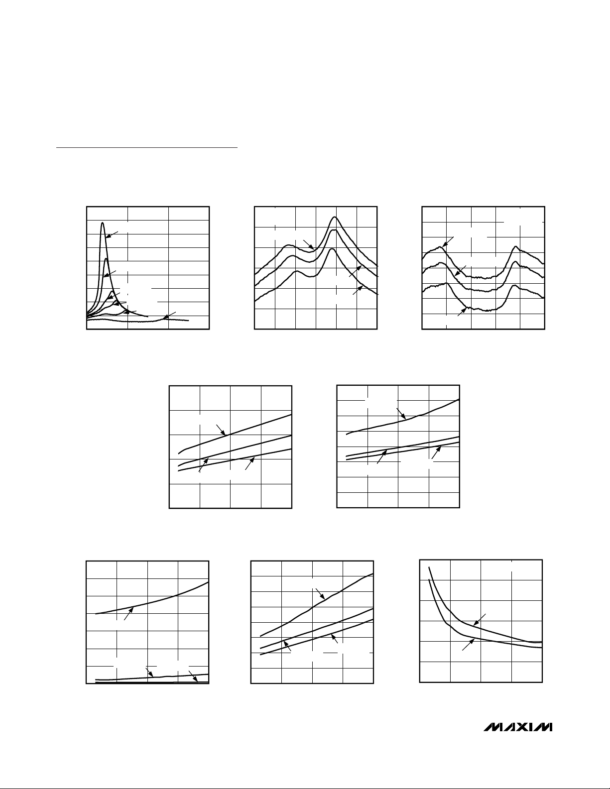
Typical Operating Characteristics (continued)
(VCC= 3.0V, TA = +25°C, unless otherwise noted.)
MAX4852H
ON-RESISTANCE vs. COM VOLTAGE
MAX4850 toc10
COM VOLTAGE (V)
ON-RESISTANCE (Ω)
42
5
10
15
20
25
30
35
40
45
0
06
VCC = 1.8V
7Ω SWITCH
VCC = 2.0V
VCC = 2.3V
VCC = 2.5V
VCC = 3.0V
VCC = 5.0V
MAX4852H
ON-RESISTANCE vs. COM VOLTAGE
MAX4850 toc11
COM VOLTAGE (V)
ON-RESISTANCE (Ω)
2.52.01.51.00.5
3
4
5
6
7
8
2
0 3.0
VCC = 3.0V
7Ω SWITCH
TA = +85°C
TA = +25°C
TA = -40°C
MAX4852H
ON-RESISTANCE vs. COM VOLTAGE
MAX4850 toc12
COM VOLTAGE (V)
ON-RESISTANCE (Ω)
431 2
2.0
2.5
3.0
3.5
4.0
4.5
5.0
5.5
1.5
05
VCC = 5.0V
7Ω SWITCH
TA = +85°C
TA = +25°C
TA = -40°C
MAX4850
SUPPLY CURRENT vs. SUPPLY VOLTAGE
MAX4850 toc13
SUPPLY VOLTAGE (V)
SUPPLY CURRENT (μA)
4.53.52.5
3
4
5
6
7
2
1.5 5.5
TA = -40°C
TA = +25°C
TA = +85°C
MAX4850H
SUPPLY CURRENT vs. SUPPLY VOLTAGE
MAX4850 toc14
SUPPLY VOLTAGE (V)
SUPPLY CURRENT (μA)
4.53.52.5
3
4
5
6
7
8
9
10
2
1.5 5.5
TA = -40°C
TA = +25°C
TA = +85°C
TA = -40°C
TA = +25°C
TA = +85°C
MAX4852
SUPPLY CURRENT vs. SUPPLY VOLTAGE
MAX4850 toc15
SUPPLY VOLTAGE (V)
SUPPLY CURRENT (nA)
4.53.52.5
0.5
1.0
1.5
2.0
2.5
3.0
3.5
0
1.5 5.5
TA = -40°C
TA = +85°C
TA = +25°C
MAX4852H
SUPPLY CURRENT vs. SUPPLY VOLTAGE
MAX4850 toc16
SUPPLY VOLTAGE (V)
SUPPLY CURRENT (μA)
4.53.52.5
3.5
4.0
4.5
5.0
5.5
6.0
6.5
7.0
3.0
1.5 5.5
TA = -40°C
TA = +25°C
TA = +85°C
TURN-ON/TURN-OFF TIME
vs. SUPPLY VOLTAGE
MAX4850 toc17
SUPPLY VOLTAGE (V)
TURN-ON/TURN-OFF TIME (ns)
4.53.52.5
10
20
30
40
50
60
0
1.5 5.5
t
ON
t
OFF
3.5Ω SWITCH
Page 7
MAX4850/MAX4850H/MAX4852/MAX4852H
Dual SPDT Analog Switches with
Over-Rail Signal Handling
_______________________________________________________________________________________ 7
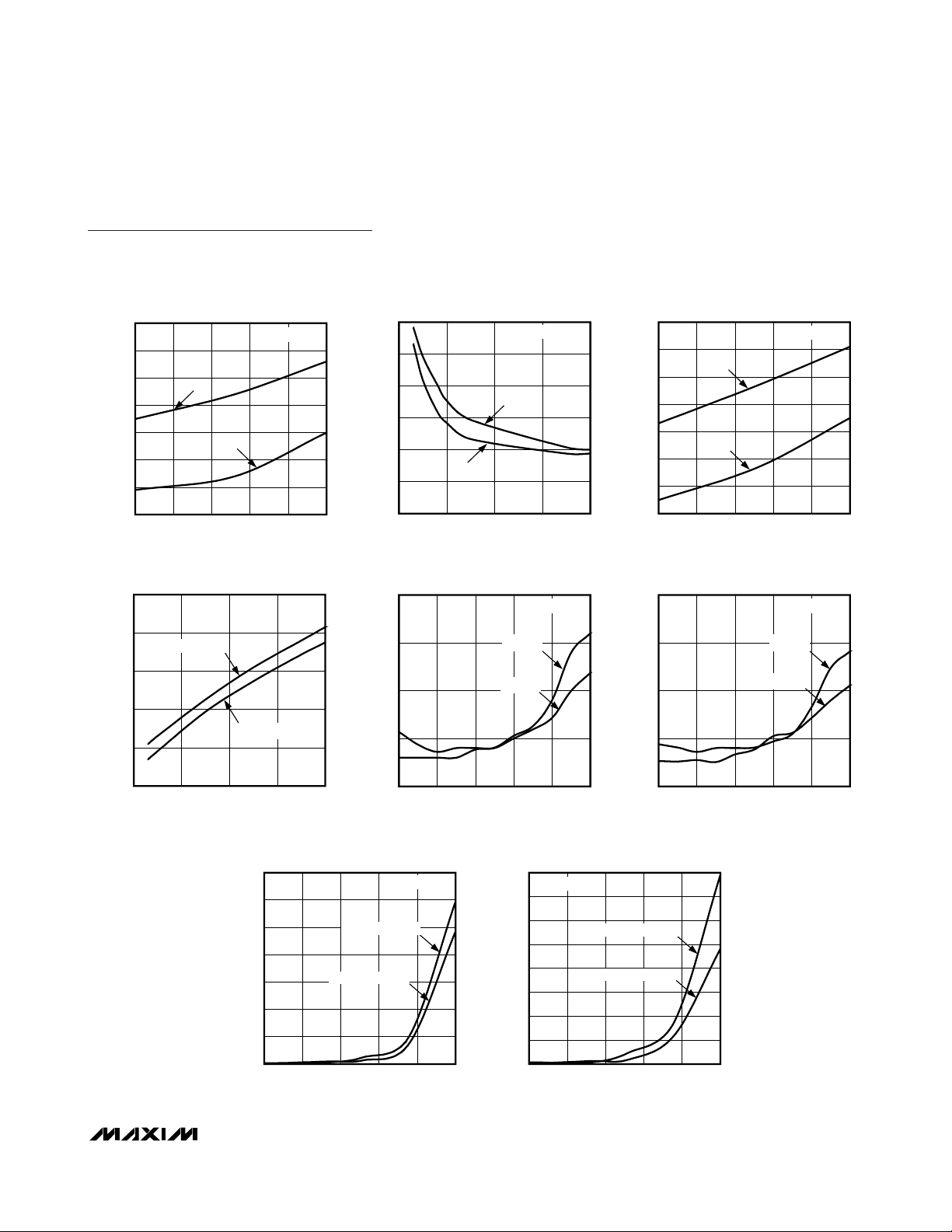
Typical Operating Characteristics (continued)
(VCC= 3.0V, TA = +25°C, unless otherwise noted.)
TURN-ON/TURN-OFF TIME
vs. TEMPERATURE
34
32
30
28
26
24
TURN-ON/TURN-OFF TIME (ns)
22
20
-40 85
t
ON
t
TEMPERATURE (°C)
3.5Ω SWITCH
MAX4850 toc18
OFF
TURN-ON/TURN-OFF TIME (ns)
603510-15
LOGIC THRESHOLD vs. SUPPLY VOLTAGE
1.6
1.4
1.2
1.0
LOGIC THRESHOLD (V)
0.8
VIN RISING
VIN FALLING
MAX4850 toc21
CHARGE INJECTION (pC)
TURN-ON/TURN-OFF TIME
vs. SUPPLY VOLTAGE
60
50
40
30
20
t
10
0
1.5 5.5
OFF
SUPPLY VOLTAGE (V)
t
ON
7Ω SWITCH
4.53.52.5
CHARGE INJECTION vs. COM VOLTAGE
40
30
20
10
3.5Ω SWITCH
VCC = 3V
VCC = 5V
34
32
MAX4850 toc19
30
28
26
24
TURN-ON/TURN-OFF TIME (ns)
22
20
40
MAX4850 toc22
30
20
CHARGE INJECTION (pC)
10
TURN-ON/TURN-OFF TIME
vs. TEMPERATURE
7Ω SWITCH
t
ON
t
OFF
-40 85
TEMPERATURE (°C)
603510-15
CHARGE INJECTION vs. COM VOLTAGE
7Ω SWITCH
VCC = 3V
VCC = 5V
MAX4850 toc20
MAX4850 toc23
0.6
1.5 5.5
SUPPLY VOLTAGE (V)
4.53.52.5
LEAKAGE CURRENT vs. TEMPERATURE
1.4
1.2
1.0
0.8
0.6
LEAKAGE CURRENT (nA)
0.4
0.2
0
-40 85
0
COM ON-LEAKAGE
COM OFF-LEAKAGE
TEMPERATURE (°C)
05
COM VOLTAGE (V)
4321
0
05
COM VOLTAGE (V)
LEAKAGE CURRENT vs. TEMPERATURE
3.5Ω SWITCH
603510-15
1.6
1.4
MAX4850 toc24
1.2
1.0
0.8
0.6
LEAKAGE CURRENT (nA)
0.4
0.2
7Ω SWITCH
COM ON-LEAKAGE
COM OFF-LEAKAGE
0
-40 85
TEMPERATURE (°C)
6035-15 10
MAX4850 toc25
4321
Page 8
MAX4850/MAX4850H/MAX4852/MAX4852H
Dual SPDT Analog Switches with
Over-Rail Signal Handling
8 _______________________________________________________________________________________
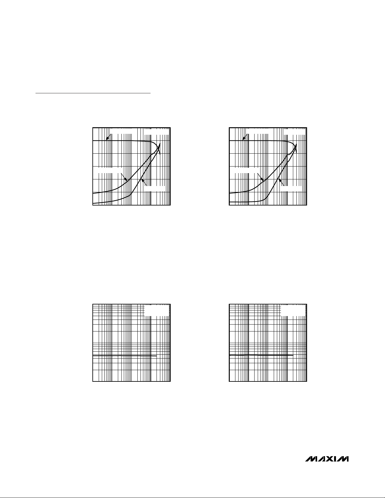
Typical Operating Characteristics (continued)
(VCC= 3.0V, TA = +25°C, unless otherwise noted.)
20
0
-20
-40
-60
FREQUENCY RESPONSE (dB)
-80
-100
0.1 1000
ON-RESPONSE
OFF-RESPONSE
3.5Ω SWITCH
CROSSTALK
FREQUENCY (MHz)
TOTAL HARMONIC DISTORTION
vs. FREQUENCY
FREQUENCY RESPONSE
1
3.5Ω SWITCH
R
100101
= 600Ω
L
MAX4850 toc26
MAX4850 toc28
20
0
-20
-40
-60
FREQUENCY RESPONSE (dB)
-80
-100
0.1 1000
ON-RESPONSE
OFF-RESPONSE
CROSSTALK
FREQUENCY (MHz)
TOTAL HARMONIC DISTORTION
vs. FREQUENCY
1
FREQUENCY RESPONSE
7Ω SWITCH
100101
7Ω SWITCH
= 600Ω
R
L
MAX4850 toc27
MAX4850 toc29
0.1
THD (%)
0.1
THD (%)
0.01
10 100k
FREQUENCY (Hz)
10k1k100
0.01
10 100k
FREQUENCY (Hz)
10k1k100
Page 9
MAX4850/MAX4850H/MAX4852/MAX4852H
Dual SPDT Analog Switches with
Over-Rail Signal Handling
_______________________________________________________________________________________ 9
Typical Operating Characteristics (continued)
(VCC= 3.0V, TA = +25°C, unless otherwise noted.)
COMPARATOR THRESHOLD
vs. TEMPERATURE
1.10
VCC = 3.0V
1.08
1.06
1.04
COMPARATOR THRESHOLD (V)
1.02
1.00
V
RISING
CMPI_
V
FALLING
CMPI_
-40 85
TEMPERATURE (°C)
COMPARATOR THRESHOLD
VCC = 5.0V
vs. TEMPERATURE
V
RISING
CMPI_
V
FALLING
CMPI_
TEMPERATURE (°C)
MAX4850 toc31
603510-15
1.750
MAX4850 toc30
603510-15
1.725
1.700
1.675
1.650
COMPARATOR THRESHOLD (V)
1.625
1.600
-40 85
V
2V/div
V
COM
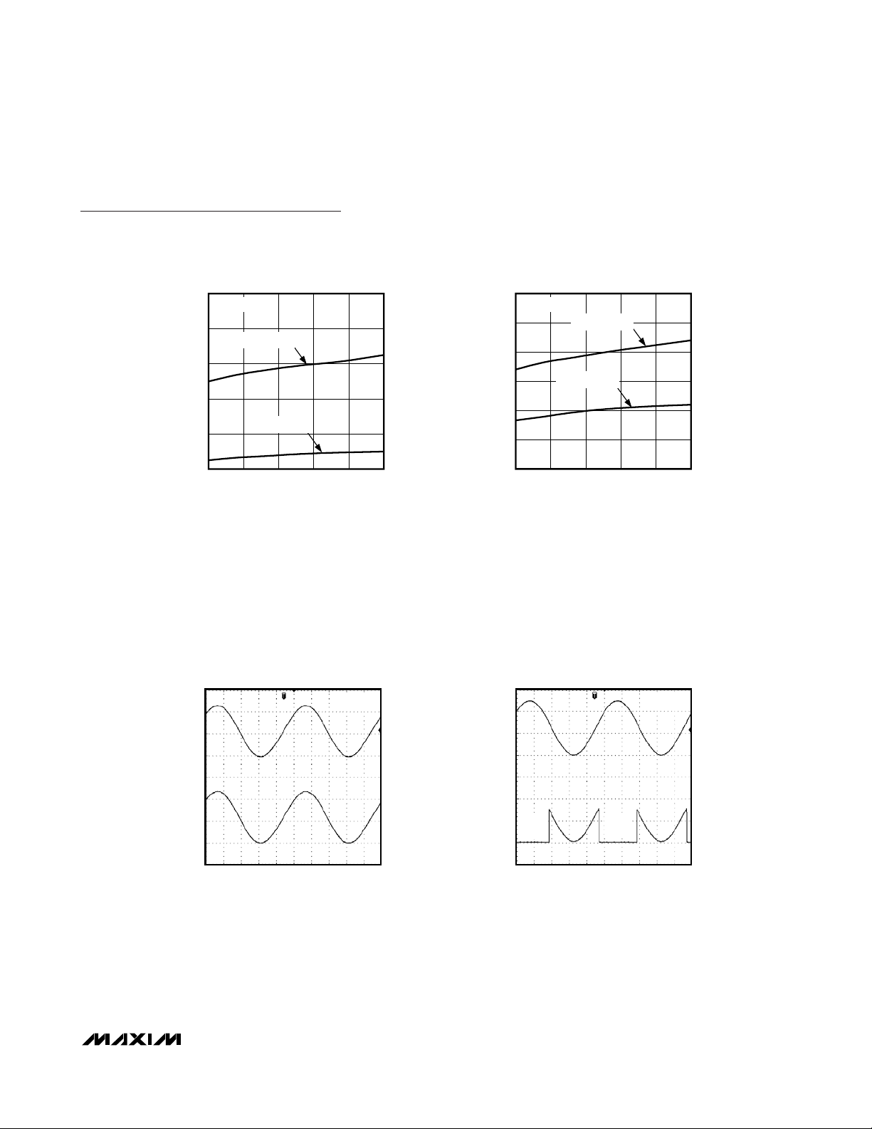
MAX4850/MAX4852
SWITCH PASSING SIGNALS
ABOVE SUPPLY VOLTAGE
NC
0V
0V
200μs/div
MAX4850 toc32
VCC = 3.0V
V
2V/div
V
COM
NC
0V
0V
MAX4850H/MAX4852H
SWITCH ENTERING
HIGH-IMPEDANCE STATE
HI-Z
STATE
200μs/div
HI-Z
STATE
MAX4850 toc33
VCC = 3.0V
Page 10
MAX4850/MAX4850H/MAX4852/MAX4852H
Dual SPDT Analog Switches with
Over-Rail Signal Handling
10 ______________________________________________________________________________________
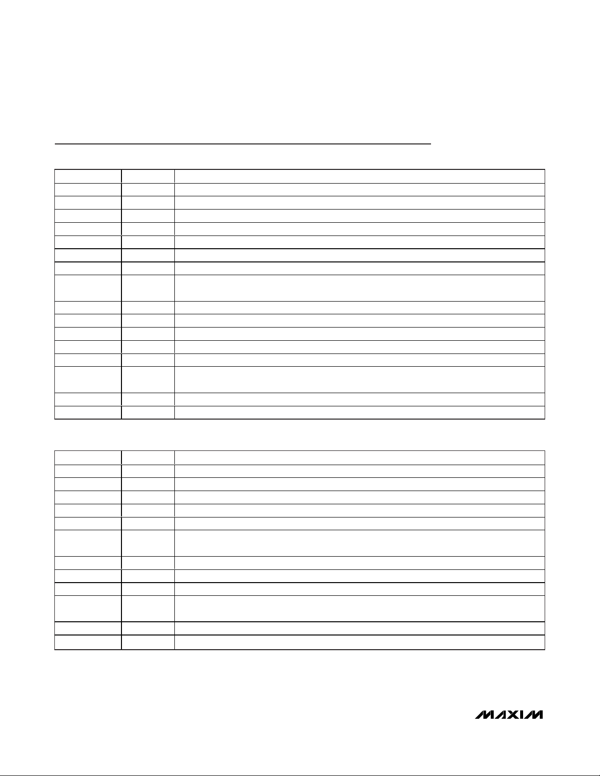
Pin Descriptions
MAX4850/MAX4850H
MAX4852/MAX4852H
PIN NAME FUNCTION
1, 8 N.C. No Connection. Not internally connected.
2 CIN1 Inverting Input for Comparator 1
3 CIN2 Inverting Input for Comparator 2
4 COM1 Common Terminal for Analog Switch 1
5 NO1 Normally Open Terminal for Analog Switch 1
6 GND Ground
7 NC2 Normally Closed Terminal for Analog Switch 2
9 IN2
10 COM2 Common Terminal for Analog Switch 2
11 COUT1 Output for Comparator 1
12 NO2 Normally Open Terminal for Analog Switch 2
13 COUT2 Output for Comparator 2
14 V
15 IN1
16 NC1 Normally Closed Terminal for Analog Switch 1
EP — Exposed Paddle. Connect to PC board ground plane.
CC
Digital Control Input for Analog Switch 2. A logic LOW on IN2 connects COM2 to NC2 and a logic
HIGH connects COM2 to NO2.
Supply Voltage. Bypass to GND with a 0.01µF capacitor as close to the pin as possible.
Digital Control Input for Analog Switch 1. A logic LOW on IN1 connects COM1 to NC1 and a logic
HIGH connects COM1 to NO1.
PIN NAME FUNCTION
1, 2, 3, 8, 11, 13 N.C. No Connection. Not internally connected.
4 COM1 Common Terminal for Analog Switch 1
5 NO1 Normally Open Terminal for Analog Switch 1
6 GND Ground
7 NC2 Normally Closed Terminal for Analog Switch 2
9 IN2
10 COM2 Common Terminal for Analog Switch 2
12 NO2 Normally Open Terminal for Analog Switch 2
14 V
15 IN1
16 NC1 Normally Closed Terminal for Analog Switch 1
EP — Exposed Paddle. Connect to PC board ground plane.
CC
Digital Control Input for Analog Switch 2. A logic LOW on IN2 connects COM2 to NC2 and a logic
HIGH connects COM2 to NO2.
Supply Voltage. Bypass to GND with a 0.01µF capacitor as close to the pin as possible.
Digital Control Input for Analog Switch 1. A logic LOW on IN1 connects COM1 to NC1 and a logic
HIGH connects COM1 to NO1.
Page 11

Detailed Description
The MAX4850/MAX4850H/MAX4852/MAX4852H are low
on-resistance, low-voltage, analog switches that operate
from a +2V to +5.5V single supply and are fully specified
for nominal 3.0V applications. These devices feature
over-rail signal capability that allows signals up to 5.5V
with supply voltages down to 2.0V. These devices are
configured as dual SPDT switches.
These switches have low 50pF on-channel capacitance,
which allows for 12Mbps switching of the data signals for
USB 2.0 full speed/1.1 applications. The MAX485_ _ are
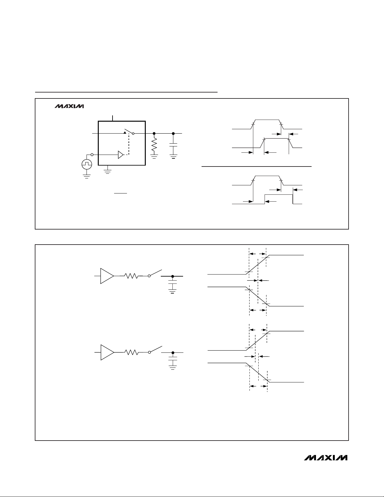
designed to switch D+ and D- USB signals with a guaranteed skew of less than 1ns (see Figure 1), as measured
from 50% of the input signal to 50% of the output signal.
The MAX4850_ feature a comparator that can be used
for headphone or mute detection. The comparator
threshold is internally generated to be approximately 1/3
of VCC.
Applications Information
Digital Control Inputs
The logic inputs (IN_) accept up to +5.5V even if the
supply voltages are below this level. For example, with a
+3.3V VCCsupply, IN_ can be driven low to GND and
high to +5.5V, allowing for mixing of logic levels in a
system. Driving IN_ rail-to-rail minimizes power con-
sumption. For a +2V supply voltage, the logic thresholds
are 0.5V (low) and 1.4V (high); for a +5V supply voltage,
the logic thresholds are 0.8V (low) and 1.8V (high).
Analog Signal Levels
The on-resistance of these switches changes very little
for analog input signals across the entire supply voltage range (see Typical Operating Characteristics). The
switches are bidirectional, so NO_, NC_, and COM_
can be either inputs or outputs.
Comparator
The positive terminal of the comparator is internally set to
V
CC
/3. When the negative terminal (CIN_) is below the
threshold (VCC/3), the comparator output (COUT_) goes
high. When CIN_ rises above VCC/3, COUT_ goes low.
The comparator threshold allows for detection of headphones since headphone audio signals are typically
biased to VCC/2.
Power-Supply Sequencing
Caution: Do not exceed the absolute maximum ratings
because stresses beyond the listed ratings may cause
permanent damage to the device.
Proper power-supply sequencing is recommended for
all CMOS devices. Always apply VCCbefore applying
analog signals, especially if the analog signal is not
current-limited.
MAX4850/MAX4850H/MAX4852/MAX4852H
Dual SPDT Analog Switches with
Over-Rail Signal Handling
______________________________________________________________________________________ 11
Page 12
MAX4850/MAX4850H/MAX4852/MAX4852H
Dual SPDT Analog Switches with
Over-Rail Signal Handling
12 ______________________________________________________________________________________
Test Circuits/Timing Diagrams
Figure 1. Switching Time
Figure 2. Input/Output Skew Timing Diagram
MAX4850_
MAX4852_
V
NO
LOGIC
INPUT
TxD+
V
CC
V
CC
NO_
IN_
GND
C
INCLUDES FIXTURE AND STRAY CAPACITANCE.
L
R
= V
V
OUT
NO (
RL + R
COM_
R
L
)
ON
A
R
s
tR < 20ns
V
CC
LOGIC
INPUT
INPUT
0V
V
OUT
0V
IN DEPENDS ON SWITCH CONFIGURATION;
INPUT POLARITY DETERMINED BY SENSE OF SWITCH.
10%
90%
V
OUT
INPUT A
INPUT A-
SWITCH
OUTPUT
SWITCH
L
C
L
B
C
L
50%
0.9 x V
t
ON
V
+ 0.5V
CC
HIGH-Z MODE
t
HIZ
NORMAL MODE NORMAL MODE
t
ri
90%
50%
t
skew_i
tF < 20ns
t
OFF
0.9 x V
0UT
t
OUT
HIZB
50%
10%
t
fi
t
ro
90%
TxD-
Rs = 39Ω
= 50pF
C
L
A-
R
s
B-
OUTPUT B
C
L
OUTPUT B-
10%
90%
50%
50%
t
skew_o
10%
t
fo
|t
|
DELAY DUE TO SWITCH FOR RISING INPUT AND RISING OUTPUT SIGNALS.
ro - tri
|t
|
DELAY DUE TO SWITCH FOR FALLING INPUT AND FALLING OUTPUT SIGNALS.
fo - tfi
|t
|
CHANGE IN SKEW THROUGH THE SWITCH FOR OUTPUT SIGNALS.
skew_o
|
|t
CHANGE IN SKEW THROUGH THE SWITCH FOR INPUT SIGNALS.
skew_i
Page 13
MAX4850/MAX4850H/MAX4852/MAX4852H
Dual SPDT Analog Switches with
Over-Rail Signal Handling
______________________________________________________________________________________ 13
MAX4850_
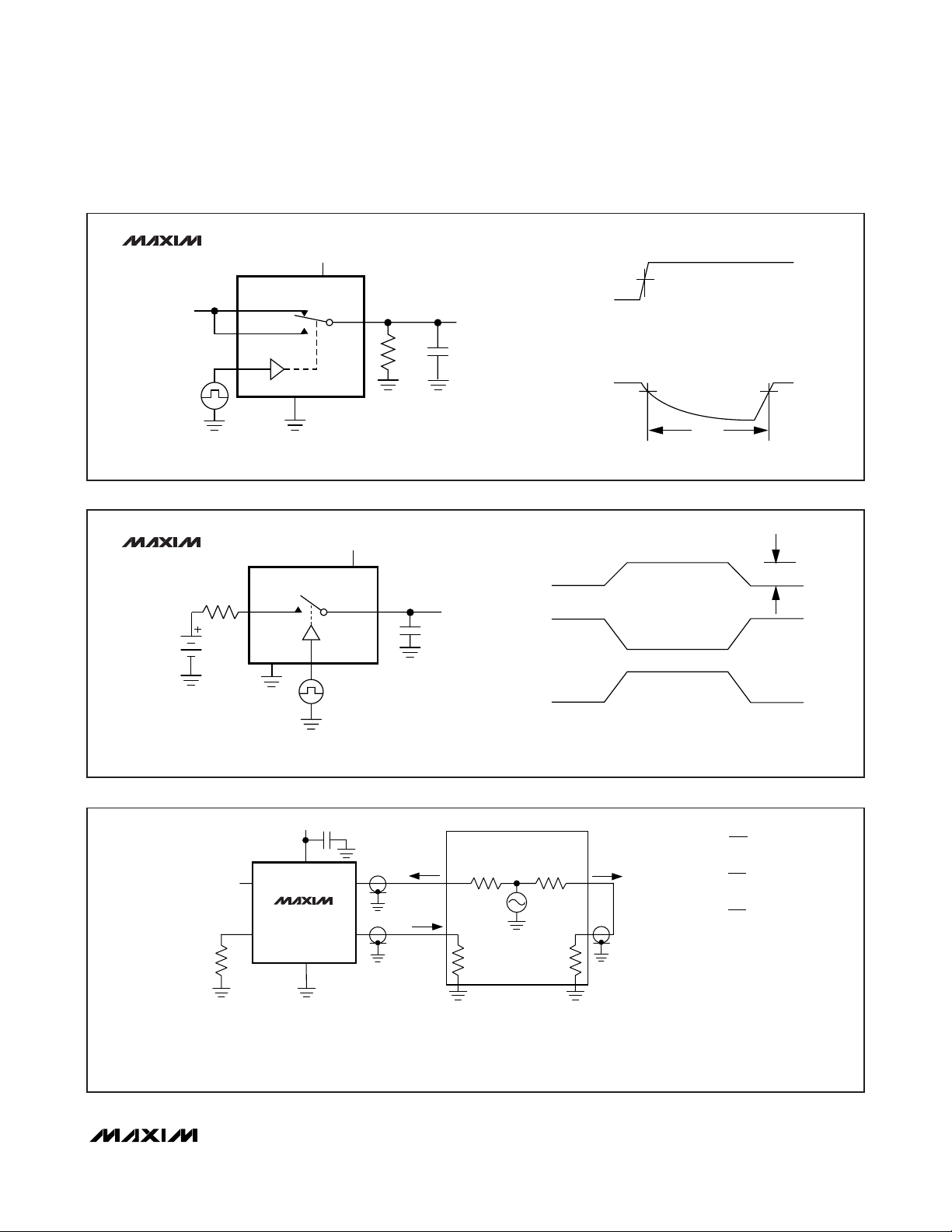
Figure 3. Break-Before-Make Interval
Figure 4. Charge Injection
Figure 5. On-Loss, Off-Isolation, and Crosstalk
MAX4852_
V
N_
NC_
NO_
IN_
V
CC
V
CC
V
COM_
OUT
R
L
C
L
LOGIC
INPUT
V
CC
50%
0V
LOGIC
INPUT
C
L
GND
INCLUDES FIXTURE AND STRAY CAPACITANCE.
MAX4850_
MAX4852_
R
GEN
NC_
OR NO_
V
GEN
GND
0V OR V
50Ω
IN_
CC
MAX4850_
MAX4852_
NC1
+5V
V
GND
0.9 x V
OUT
OFF
V
CC
V
CC
COM_
V
OUT
t
BBM
ΔV
OUT
V
OUT
V
OUT
C
L
IN
OFF
ON
IN_
Q = (ΔV
ON
OUT
OFF
)(CL)
TO V
V
IL
IH
OFF
IN
LOGIC-INPUT WAVEFORMS INVERTED FOR SWITCHES
THAT HAVE THE OPPOSITE LOGIC SENSE.
10nF
NETWORK
ANALYZER
CC
COM1
NO1*
V
IN
V
OUT
50Ω
MEAS REF
50Ω 50Ω
50Ω
OFF-ISOLATION = 20log
ON-LOSS = 20log
CROSSTALK = 20log
V
OUT
V
IN
V
OUT
V
IN
V
OUT
V
IN
MEASUREMENTS ARE STANDARDIZED AGAINST SHORTS AT IC TERMINALS.
OFF-ISOLATION IS MEASURED BETWEEN COM_ AND "OFF", NO_ OR NC_ TERMINAL ON EACH SWITCH.
ON-LOSS IS MEASURED BETWEEN COM_ AND "ON", NO_ OR NC_ TERMINAL ON EACH SWITCH.
CROSSTALK IS MEASURED FROM ONE CHANNEL TO THE OTHER CHANNEL.
SIGNAL DIRECTION THROUGH SWITCH IS REVERSED; WORST VALUES ARE RECORDED.
*FOR CROSSTALK THIS PIN IS NO2.
NC2 AND COM2 ARE OPEN.
Page 14
MAX4850/MAX4850H/MAX4852/MAX4852H
Dual SPDT Analog Switches with
Over-Rail Signal Handling
14 ______________________________________________________________________________________
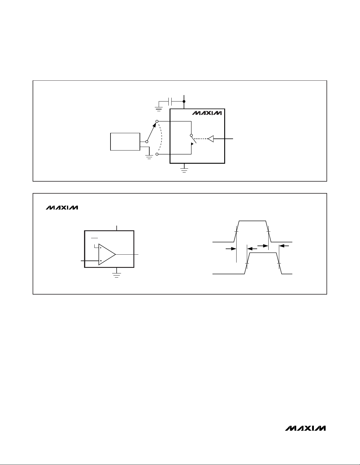
Figure 6. Channel Off-/On-Capacitance
Figure 7. Comparator Switching Time
V
CC
10nF
V
CC
CAPACITANCE
METER
f = 1MHz
COM_
NC_ OR
NO_
MAX4850_
MAX4852_
IN
GND
V
OR V
IL
IH
MAX4850_
V
CIN_
NO_
CIN_
V
TH
V
CC
3
= VCC/3
V
CC
V
CC
GND
COUT_
V
COUT_
COMPARATOR
INPUT (V
COMPARATOR
OUTPUT (V
CIN_
COUT_
VTH + 100mV
)
V
- 100mV
TH
V
)
OUT
50%
t
COMP
50%
0V
tR < 20ns
t
50%
F
< 20ns
50%
t
COMP
Page 15
MAX4850/MAX4850H/MAX4852/MAX4852H
Dual SPDT Analog Switches with
Over-Rail Signal Handling
______________________________________________________________________________________ 15
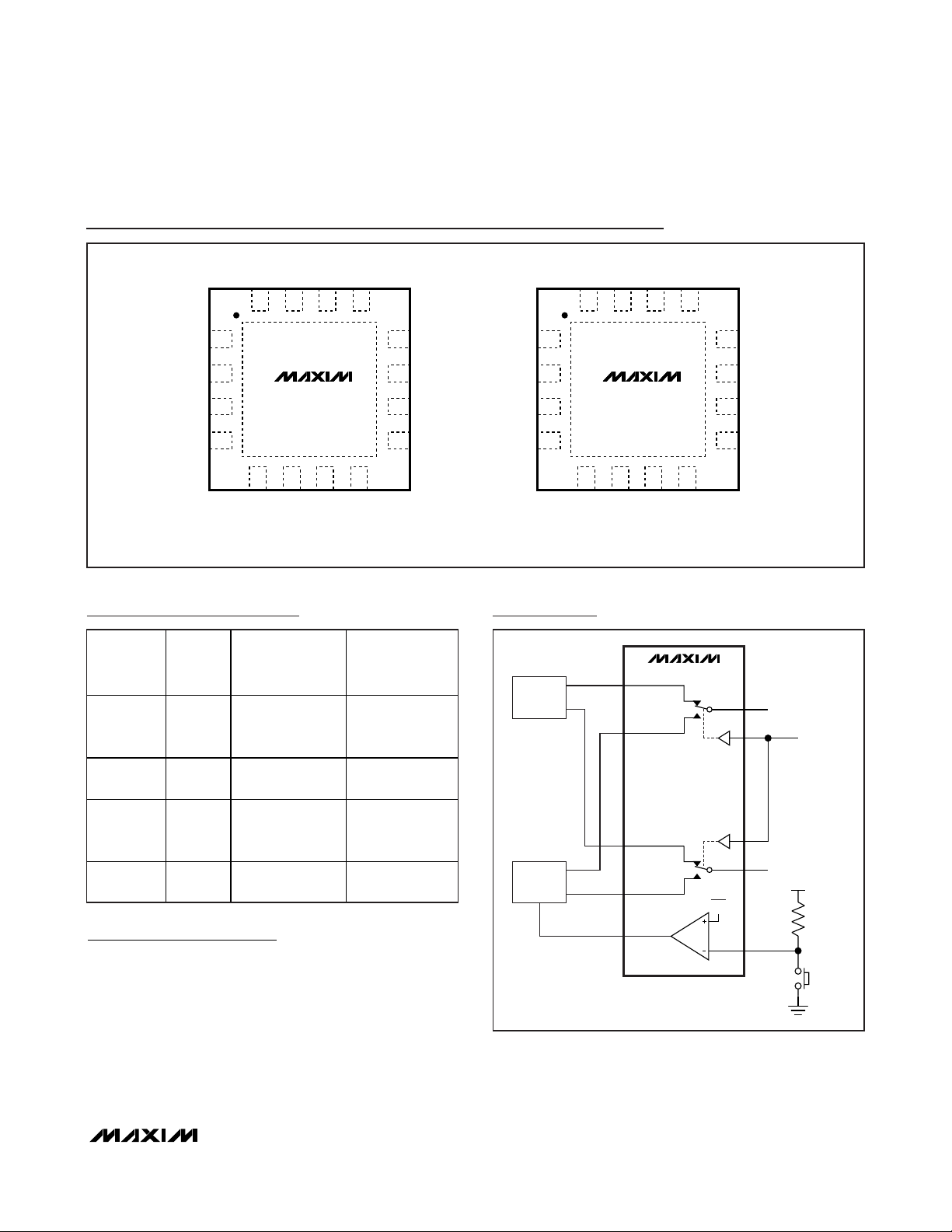
Pin Configurations
Selector Guide
Chip Information
TRANSISTOR COUNT: 735
PROCESS: CMOS
Typical Operating Circuit
TOP VIEW
N.C.
CIN1
CIN2
COM1
NC1
16
1
2
3
4
5678
NO1
THIN QFN THIN QFN
CONNECT EXPOSED PADDLE TO GROUND.
R
ON
PART
NC_/NO_
COMPARATORS
(Ω)
MAX4850 3.5/3.5 2
IN1
VCCCOUT2
15 14 13
NO2
12
COUT1
11
MAX4850
MAX4850H
GND
NC2
N.C.
COM2
10
IN2
9
OVER-RAIL
HANDLING
Input signal
passes through
the switch
N.C.
N.C.
N.C.
COM1
DATA
SOURCE
NC1
IN1
VCCN.C.
16
15 14 13
1
2
NO2
12
N.C.
11
MAX4852
3
4
MAX4852H
5678
NO1
GND
NC2
N.C.
COM2
10
IN2
9
OUT+
OUT-
NC1
NO1
MAX4850_
COM1
IN1
INPUT
SELECT
MAX4850H 3.5/3.5 2
MAX4852 3.5/7 —
MAX4852H 3.5/7 —
High-impedance
switch input
Input signal
passes through
the switch
High-impedance
switch input
MUTE
AUDIO
SOURCE
OUT+
OUT-
NC2
NO2
COUT
IN2
COM2
V
CIN
CC
MUTE
BUTTON
V
CC
3
Page 16
MAX4850/MAX4850H/MAX4852/MAX4852H
Dual SPDT Analog Switches with
Over-Rail Signal Handling
Maxim cannot assume responsibility for use of any circuitry other than circuitry entirely embodied in a Maxim product. No circuit patent licenses are
implied. Maxim reserves the right to change the circuitry and specifications without notice at any time.
16 ____________________Maxim Integrated Products, 120 San Gabriel Drive, Sunnyvale, CA 94086 408-737-7600
© 2004 Maxim Integrated Products is a registered trademark of Maxim Integrated Products.
Package Information
(The package drawing(s) in this data sheet may not reflect the most current specifications. For the latest package outline information
go to www.maxim-ic.com/packages
.)
MARKING
D/2
D
0.10 C 0.08 C
8L 3x3
PKG
MIN.
NOM. MAX.
REF. MIN.
0.70 0.75 0.80
A
b
0.25 0.30 0.35
3.00 3.10
D
2.90
2.90 3.00 3.10
E
e
0.65 BSC.
0.55 0.75
L
0.35
8
ND
2
2
NE
A1
0
0.02
A2
k
0.05
0.20 REF
-
-
0.25
E/2
AAAA
C
L
12L 3x3
NOM. MAX. NOM.
0.70
0.75
0.80
0.20
0.25
0.30
2.90
3.00
3.10
3.00
2.90
3.10
0.50 BSC.
0.55
0.45
0.65
12N
3
0
0.0230.05
0.20 REF
-
0.25
E
A
A2
A1
MIN. MAX.
0.70
0.20
2.90
2.90
0.30
040.02
-
0.25
16L 3x3
0.75
0.25
3.00
3.00
0.50 BSC.
0.40
16
4
0.20 REF
-
(NE - 1) X e
E2/2
MAX.
1.25
1.25
0.95
0.95
1.25
D2/2
D2
b
C
L
e
21-0136
JEDEC
PIN ID
WEED-1
0.35 x 45°
WEED-11.25
0.35 x 45°
0.35 x 45°
WEED-2
0.225 x 45°
WEED-2
0.225 x 45°
WEED-2
0.35 x 45°
WEED-2
0.35 x 45° WEED-2
0.10 M C A B
L
12x16L QFN THIN.EPS
1
I
2
(ND - 1) X e
C
L
L
PKG.
CODES
0.80
0.30
TQ833-1 1.250.25 0.70 0.35 x 45° WEEC1.250.700.25
3.10
T1233-1
3.10
T1233-3
T1233-4
0.50
T1633-2 0. 95
T1633F-3
T1633FH-3 0.65 0.80 0.95
T1633-4 0. 95
0.05
T1633-5 0. 95
-
e
k
L
C
L
e
EXPOSED PAD VARIATIONS
D2
MIN.
NOM.
MAX.
MIN.
1.25
0.95
1.10
0.95
1.25
1.10
0.95 1.10 0.35 x 45°1.2 5 WEED-10.95
1.251.10
0.95
1.25
1.10
0.65
0.95
0.95
0.80
0.65
0.65 0.80
1.10 1.25 0.95 1.10
1.25
0.95
1.10
E2
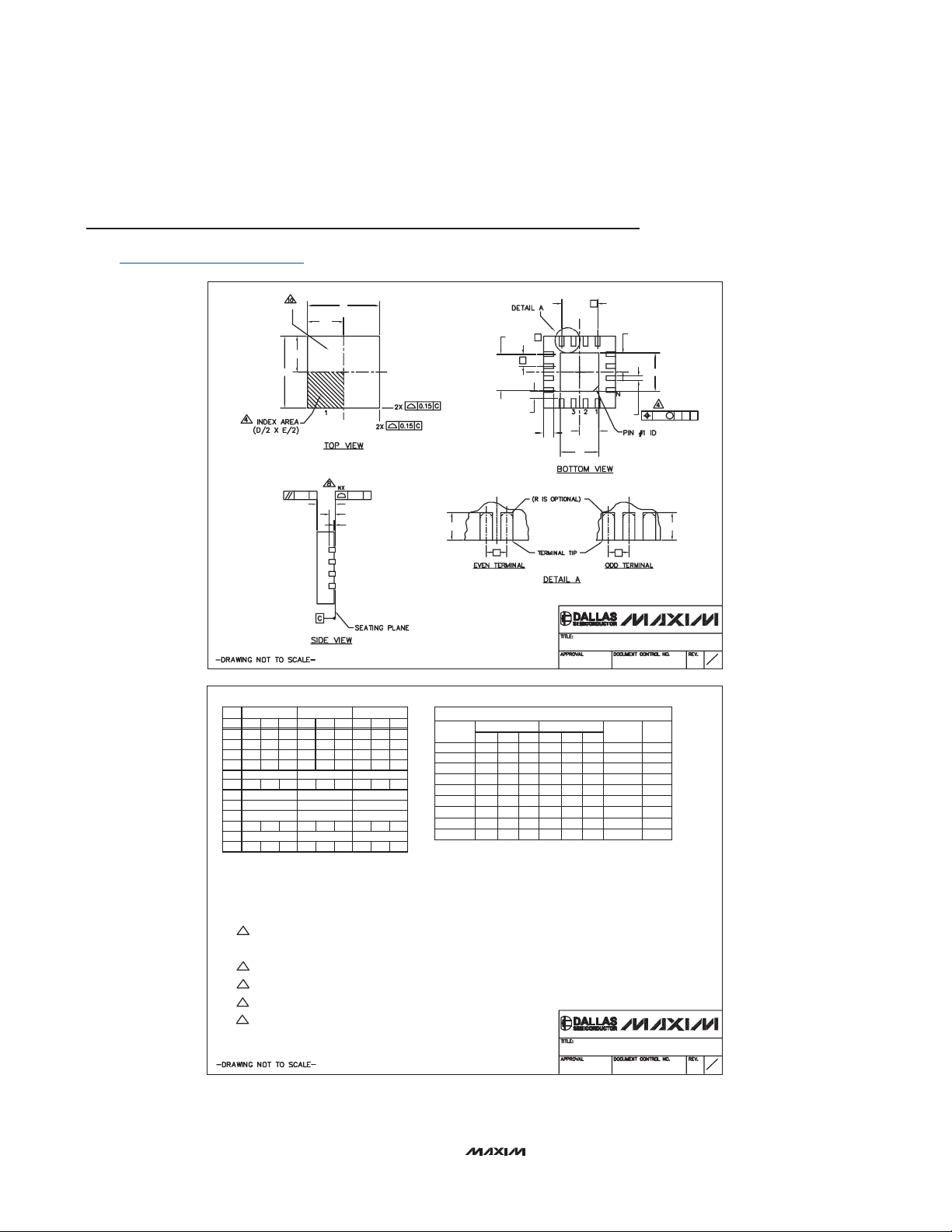
PACKAGE OUTLINE
8, 12, 16L THIN QFN, 3x3x0.8mm
E2
NOM.
1.10
1.100.95
1.10
0.80
1.10 1.25
NOTES:
1. DIMENSIONING & TOLERANCING CONFORM TO ASME Y14.5M-1994.
2. ALL DIMENSIONS ARE IN MILLIMETERS. ANGLES ARE IN DEGREES.
3. N IS THE TOTAL NUMBER OF T ERMINALS.
4. THE TERMINAL #1 IDENTIFIER AND TERMINAL NUMBERING CONVENTION SHALL CONFORM TO
JESD 95-1 SPP-012. DETAILS OF TERMINAL #1 IDENTIFIER ARE OPTIONAL, BUT MUST BE LOCATED
WITHIN THE ZONE INDICATED. THE TERMINAL #1 IDENTIFIER MAY BE EITHER A MOLD OR
MARKED FEATURE.
5. DIMENSION b APPLIES TO METALLIZED TERMINAL AND IS MEASURED BETWEEN 0.20 mm AND 0.25 mm
FROM TERMINAL TIP.
6. ND AND NE REFER TO THE NUMBER OF TERMINALS ON EACH D AND E SIDE RESPECTIVELY.
7. DEPOPULATION IS POSSIBLE IN A SYMMETRICAL FASHION.
8. COPLANARITY APPLIES TO THE EXPOSED HEAT SINK SLUG AS WELL AS THE TERMINALS .
9. DRAWING CONFORMS TO JEDEC MO220 REVISION C.
10. MARKING IS FOR PACKAGE ORIENTATION REFERENCE ONLY.
11. NUMBER OF LEADS SHOWN ARE FOR REFERENCE ONLY.
12. WARPAGE NOT TO EXCEED 0.10mm.
PACKAGE OUTLINE
8, 12, 16L THIN QFN, 3x3x0.8mm
21-0136
2
I
2
 Loading...