

Page 1
General Description
The MAX4729/MAX4730 single-pole/double-throw
(SPDT) switches operate from a single supply ranging
from +1.8V to +5.5V. These switches provide low 3.5Ω
on-resistance (RON), as well as 0.45Ω RONflatness with
a +2.7V supply. These devices typically consume only
1nA of supply current, making them ideal for use in lowpower, portable applications. The MAX4729/MAX4730
feature low-leakage currents over the extended temperature range, TTL/CMOS-compatible digital logic, and
excellent AC characteristics.
The MAX4729/MAX4730 are available in small 6-pin
SC70 and 6-pin µDFN packages. The MAX4729/
MAX4730 are offered in three pinout configurations to
ease design. The MAX4729/MAX4730 are specified
over the extended -40°C to +85°C temperature range.
Applications
Battery-Operated Equipment
Audio and Video-Signal Routing
Low-Voltage Data-Acquisition Systems
Sample-and-Hold Circuits
Communications Circuits
Relay Replacement
Features
♦ Low 3.5Ω RON(+2.7V Supply)
♦ 0.45Ω RONFlatness (+2.7V Supply)
♦ 0.05Ω R
ON
Match Between Channels (+2.7V
Supply)
♦ Tiny SC70 and µDFN Packages
♦ -3dB Bandwidth: 300MHz
♦ Low On-Capacitance: 19.5pF
♦ 0.036% Total Harmonic Distortion
♦ Low Supply Current: 1nA
♦ +1.8V to +5.5V Single-Supply Operation
MAX4729/MAX4730
Low-Voltage 3.5ΩΩ, SPDT,
CMOS Analog Switches
________________________________________________________________ Maxim Integrated Products 1
5
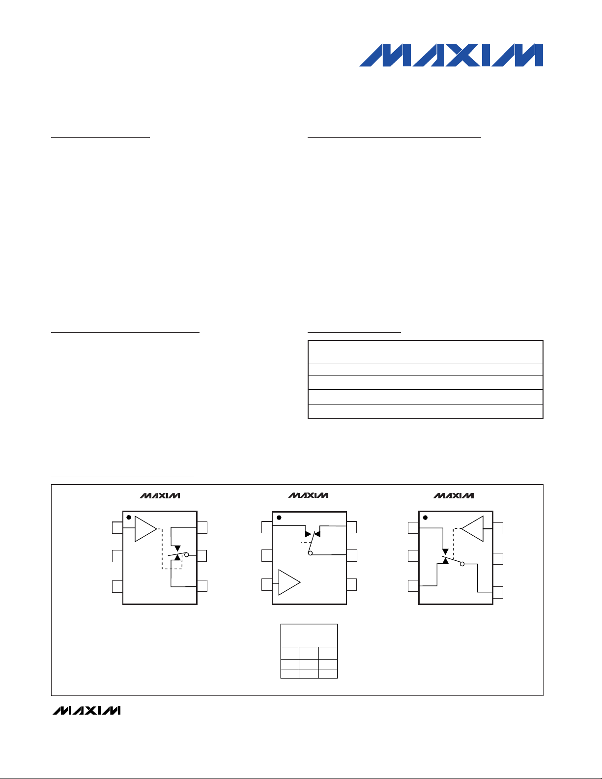
COM
TOP VIEW
V+
NC
SWITCHES SHOWN FOR LOGIC 0 INPUT.
GND
1
6
NO
IN
SC70
2
3
4
V+
GND
IN
16
NC
NO
µDFN
2
3
4
GND
NC
1
6 IN
5 V+
NO
SC70
µDFN
2
3
4
MAX4729
MAX4729
MAX4730
COM
NO
OFF
ON
NC
ON
OFF
0
1
MAX4729/
MAX4730
IN
5
COM
Pin Configurations/Functional Diagrams/Truth Table
Ordering Information
19-3284; Rev 1; 2/05
For pricing, delivery, and ordering information, please contact Maxim/Dallas Direct! at
1-888-629-4642, or visit Maxim’s website at www.maxim-ic.com.
PART
PIN-
TOP
MARK
MAX4729EXT-T
6 SC70-6 ABU
MAX4729ELT-T*
6 µDFN-6 —
MAX4730EXT-T
6 SC70-6 ABV
MAX4730ELT-T*
6 µDFN-6 —
*Future product—contact factory for availability.
TEMP RANGE
-40ºC to +85ºC
-40ºC to +85ºC
-40ºC to +85ºC
-40ºC to +85ºC
PACKAGE
Page 2
MAX4729/MAX4730
Low-Voltage 3.5ΩΩ, SPDT,
CMOS Analog Switches
2 _______________________________________________________________________________________
ABSOLUTE MAXIMUM RATINGS
Stresses beyond those listed under “Absolute Maximum Ratings” may cause permanent damage to the device. These are stress ratings only, and functional
operation of the device at these or any other conditions beyond those indicated in the operational sections of the specifications is not implied. Exposure to
absolute maximum rating conditions for extended periods may affect device reliability.
(All voltages referenced to ground)
V+, IN .......................................................................-0.3V to +6V
COM, NO, NC (Note 1)..................................-0.3V to (V+ +0.3V)
Continuous Current (IN, V+, GND) ...................................±30mA
Continuous Current (COM, NO, NC) ................................±80mA
Peak Current COM, NO, NC
(Pulsed at 1ms, 10% Duty Cycle)................................±150mA
Continuous Power Dissipation (T
A
= +70°C)
6-Pin µDFN (derate 2.1mW/°C above +70°C) ..............168mW
6-Pin SC70 (derate 3.1mW/°C above +70°C)...............245mW
Operating Temperature Range ...........................-40°C to +85°C
Maximum Junction Temperature .....................................+150°C
Storage Temperature Range .............................-65°C to +150°C
Lead Temperature (soldering, 10s) .................................+300°C
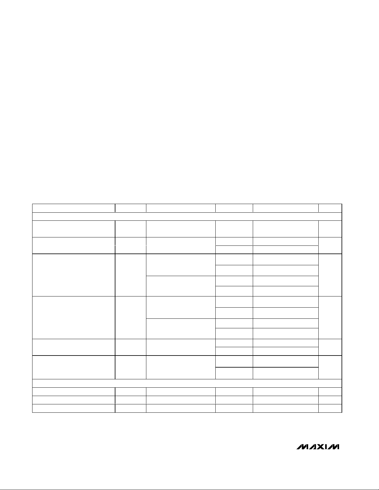
ELECTRICAL CHARACTERISTICS
(V+ = +2.7V to +3.6V, VIH= +2.0V, VIL= +0.4V, TA= T
MIN
to T
MAX
, unless otherwise noted. Typical values are at TA= +25°C.) (Note 2)
PARAMETER
SYMBOL
CONDITIONS T
A
MIN
TYP
MAX
UNITS
ANALOG SWITCH
Analog Signal Range
V
COM
,
0V+V
+25°C 3.5 5.5
On-Resistance (Note 6) R
ON
V+ = 2.7V, I
COM
= 10mA,
V
NO
or VNC = 0V to V+
5.7
Ω
+25°C
V+ = 2.7V, I
COM
= 10mA,
V
NO
or VNC = 0.7V, 1.2V,
2V (MAX4729)
0.2
+25°C 0.2
On-Resistance Match Between
Channels (Notes 3, 6)
∆R
ON
V+ = 2.7V, I
COM
= 10mA,
V
NO
or VNC = 0.7V, 1.2V,
2V (MAX4730)
Ω
+25°C 0.8 1.5
V+ = 2.7V, I
COM
= 10mA,
V
NO
or VNC = 0.7V, 1.2V,
2V (MAX4729)
2.2
+25°C
On-Resistance Flatness (Note 4)
)
V+ = 2.7V, I
COM
= 10mA,
V
NO
or VNC = 0.7V, 1.2V,
2V (MAX4730)
1.3
Ω
+25°C -2
+2
NO, NC Off-Leakage Current
I
NO (OFF),
)
V+ = 3.3V, V
COM
= 1V, 3V,
V
NO
or VNC = 3V, 1V
-3 +3
nA
+25°C -3
+3
COM On-Leakage Current
)
V+ = 3.3V, V
COM
= 1V or
3V, V
NO
or VNC = 1V, 3V, or
float
-4 +4
nA
DIGITAL INPUTS
Input Logic High V
IH
2.0 V
Input Logic Low V
IL
0.4 V
Input Leakage Current I
IN
VIN = 0V or 3.6V
-1
+1 µA
Note 1: Signals on NO, NC, or COM exceeding V+ or GND are clamped by internal diodes. Signals on IN exceeding GND are
clamped by an internal diode. Limit forward-diode current to maximum current rating.
V
NO, VNC
R
FLAT(ON
I
NC (OFF
I
COM (ON
T
to T
MIN
MAX
0.05 0.15
T
to T
MIN
MAX
0.34
T
MIN
to T
MAX
0.37
T
to T
MIN
MAX
0.45 0.95
T
to T
MIN
MAX
+0.01
T
MIN
to T
MAX
+0.01
T
to T
MIN
MAX
T
to T
MIN
MAX
T
to T
MIN
MAX
T
to T
MIN
MAX
+0.005
Page 3
MAX4729/MAX4730
Low-Voltage 3.5ΩΩ, SPDT,
CMOS Analog Switches
_______________________________________________________________________________________ 3
PARAMETER
SYMBOL
CONDITIONS T
A
MIN
TYP
MAX
UNITS
DYNAMIC
+25°C 18 45
Turn-On Time (Note 5) t
ON
CL = 35pF, Figure 1
45
ns
+25°C 10 26
Turn-Off Time (Note 5) t
OFF
CL = 35pF, Figure 1
26
ns
+25°C 5
Break-Before-Make (Note 5)
CL = 35pF, Figure 1
1
ns
Charge Injection Q
3pC
NO, NC Off-Capacitance
C
NO(OFF)
,
)
f = 1MHz, Figure 4 6.5 pF
Switch On-Capacitance C
ON
f = 1MHz, Figure 4
pF
f = 1MHz -67
Off-Isolation (Note 7) V
ISO
VNO = VNC = 1V
RMS
, RL =
50Ω, C
L
= 5pF, Figure 2
f = 10MHz -45
dB
On-Channel Bandwidth -3dB BW Signal = 0dBm, 50Ω in and out, Figure 2
MHz
f = 1MHz -67
Crosstalk (Note 8) V
CT
NO or NC = 1V
RMS
, CL =
5pF, R
L
= 50Ω, Figure 2
f = 10MHz -52
dB
Total Harmonic Distortion THD
R
L
= 600Ω, VNC or VNO =
2V
P-P
, f = 20Hz to 20kHz
+25°C
%
POWER SUPPLY
Power-Supply Range V+ 1.8 5.5 V
+25°C
Positive Supply Current I+
1
µA
ELECTRICAL CHARACTERISTICS (continued)
(V+ = +2.7V to +3.6V, VIH= +2.0V, VIL= +0.4V, TA= T
MIN
to T
MAX
, unless otherwise noted. Typical values are at TA= +25°C.) (Note 2)
Note 2: SC70 and µDFN parts are 100% tested at T
A
= +25°C. Limits across the full-temperature range are guaranteed by design
and correlation.
Note 3: ∆R
ON
= R
ON(MAX)
- R
ON(MIN)
.
Note 4: R
ON
flatness is defined as the difference between the maximum and minimum value of on-resistance as measured over the
specified analog signal ranges.
Note 5: Guaranteed by design.
Note 6: µDFN is guaranteed by design.
Note 7: Off-Isolation = 20log10 (VO / VI), where VO is V
COM
and VI is either VNCor VNOfrom the network analyzer.
Note 8: Crosstalk is measured between the two switches.
C
NC(OFF
VNO, VNC = 2V, RL = 300Ω,
VNO, VNC = 2V, RL = 300Ω,
VNO, VNC = 2V, RL = 300Ω,
V
= 0V, R
GEN
GEN
T
to T
MIN
MAX
T
to T
MIN
MAX
T
to T
MIN
MAX
= 0, CL = 1.0nF, Figure 3
19.5
300
0.035
V+ = 5.5V, VIN = 0V or 5.5V
T
MIN
to T
MAX
0.001
Page 4

MAX4729/MAX4730
Low-Voltage 3.5ΩΩ, SPDT,
CMOS Analog Switches
4 _______________________________________________________________________________________
Typical Operating Characteristics
(TA = +25°C, unless otherwise noted.)
0
1.0
2.0
1.5
2.5
3.0
021345
ON-RESISTANCE vs. V
COM
(V+ = +5V)
MAX4729 toc04
COM VOLTAGE (V)
R
ON
(Ω)
TA = -40°C
TA = +25°C
TA = +85°C
-100
100
0
300
200
400
500
-40 10-15 35 60 85
ON/OFF-LEAKAGE CURRENT
vs. TEMPERATURE
MAX4729 toc05
TEMPERATURE (°C)
ON/OFF-LEAKAGE CURRENT (pA)
ON, VCC = 5V
OFF, VCC = 5V
ON, VCC = 3V
OFF, VCC = 3V
0
20
10
40
30
50
60
021345
CHARGE INJECTION vs. V
COM
MAX4729 toc06
V
COM
(V)
CHARGE INJECTION (pC)
1.8V
5V
3V
0
200
600
400
800
1000
-40 10-15 35 60 85
SUPPLY CURRENT vs. TEMPERATURE
MAX4729 toc07
TEMPERATURE (°C)
SUPPLY CURRENT (pA)
V+ = 5V
V+ = 3V
0.001
100
10,000
1000
100,000
1,000,000
SUPPLY CURRENT
vs. LOGIC INPUT VOLTAGE
MAX4729 toc08
LOGIC INPUT VOLTAGE (V)
SUPPLY CURRENT (nA)
02 46
10
1
0.1
0.01
V+ = 5V
V+ = 3V
0
10
5
20
15
30
25
35
tON/t
OFF
vs. SUPPLY VOLTAGE
MAX4729 toc09
SUPPLY VOLTAGE (V)
t
ON
/t
OFF
(ns)
1.5 2.5 3.5 4.5 5.5
t
ON
t
OFF
0
10
5
20
15
25
30
021345
ON-RESISTANCE vs. V
COM
MAX4729 toc01
V
COM
(V)
R
ON
(Ω)
V+ = 1.8V
V+ = 2.5V
V+ = 3V
V+ = 4.5V
V+ = 5V
0
5
10
15
20
25
30
35
40
0 0.60.3 0.9 1.2 1.5 1.8
ON-RESISTANCE vs. V
COM
(V+ = +1.8V)
MAX4729 toc02
V
COM
(V)
R
ON
(Ω)
TA = -40°C
TA = +25°C
TA = +85°C
0
1
3
2
4
5
0 1.00.5 1.5 2.0 2.5 3.0
ON-RESISTANCE vs. V
COM
(V+ = +3V)
MAX4729 toc03
V
COM
(V)
R
ON
(Ω)
TA = -40°C
TA = +25°C
TA = +85°C
Page 5

0
10
5
20
15
25
30
-40 10-15 35 60 85
MAX4729 toc10
TEMPERATURE (°C)
t
ON
/t
OFF
(ns)
V+ = 3V
tON/t
OFF
vs. TEMPERATURE
t
ON
t
OFF
V+ = 5V
V+ = 3V
V+ = 5V
OFF-ISOLATION
MAX4729 toc11
FREQUENCY (MHz)
RESPONSE (dB)
100101
-80
-70
-60
-50
-40
-30
-20
-10
0
-90
0.1 1000
V+ = 3V
V+ = 5V
50Ω IN AND OUT
CROSSTALK
MAX4729 toc12
FREQUENCY (MHz)
RESPONSE (dB)
100101
-80
-70
-60
-50
-40
-30
-20
-10
0
-90
0.1 1000
V+ = 3V
V+ = 5V
50Ω IN AND OUT
MAX4729/MAX4730
Low-Voltage 3.5ΩΩ, SPDT,
CMOS Analog Switches
_______________________________________________________________________________________ 5
ON-LOSS BANDWIDTH
MAX4729 toc13
FREQUENCY (MHz)
RESPONSE (dB)
1001010.1
-6
-5
-4
-3
-2
-1
0
-7
0.01 1000
V+ = 3V
V+ = 5V
50Ω IN AND OUT
TOTAL HARMONIC DISTORTION
vs. FREQUENCY
MAX4729 toc14
FREQUENCY (kHz)
THD (%)
1010.1
0.01
0.02
0.03
0.04
0.05
0.06
0
0.01 100
OUTPUT IMPEDANCE = 600Ω
f = 20Hz to 20kHz
V+ = 3V, V
GEN
= 3V
P-P
V+ = 3V, V
GEN
= 2V
P-P
V+ = 5V, V
GEN
= 5V
P-P
V+ = 5V, V
GEN
= 3V
P-P
TOTAL HARMONIC DISTORTION
vs. FREQUENCY
MAX4729 toc15
FREQUENCY (kHz)
THD (%)
1010.1
0.01
0.02
0.03
0.04
0.05
0.06
0
0.01 100
OUTPUT IMPEDANCE = 600Ω
MAX4730
V+ = 3V, V
GEN
= 3V
P-P
V+ = 3V, V
GEN
= 2V
P-P
V+ = 5V, V
GEN
= 5V
P-P
V+ = 5V, V
GEN
= 3V
P-P
Typical Operating Characteristics (continued)
(TA = +25°C, unless otherwise noted.)
Pin Description
PIN
MAX4729 MAX4730
SC70 µDFN SC70/µDFN
NAME FUNCTION
13 6INLogic-Control Input
22 5V+Positive Supply Voltage
34 2 GND Ground
46 3NCAnalog Switch Normally Closed Terminal
55 4 COM Analog Switch Common Terminal
61 1NOAnalog Switch Normally Open Terminal
Page 6

MAX4729/MAX4730
Low-Voltage 3.5ΩΩ, SPDT,
CMOS Analog Switches
6 _______________________________________________________________________________________
50%
0V
R
L
IN
V
IN
V+
t
OFF
0V
t
ON
C
L
V+
V
COM
MAX4729
MAX4730
GND
t
r
< 5ns
t
f
< 5ns
NO/NC
V
NO/NC
V+
OPEN
NC/NO
COM
R
L
IN
V
IN
C
L
V+
V
COM
MAX4729
MAX4730
GND
NO
V
S
V+
V
S
NC
COM
IN
50%
90%90%
V
NO/NC
V
COM
50%
0V
V+
t
BBM
IN
50%
90%
V
S
V
COM
0V
90%
t
BBM
t
BBM = tON(NC) - tOFF(NO)
OR t
BBM = tON(NO) - tOFF(NC)
Figure 1. Switching Times
Detailed Description
The MAX4729/MAX4730 single-pole/double-throw
(SPDT) switches operate from a single supply ranging
from +1.8V to +5.5V. These switches provide low 3.5Ω
on-resistance (RON), as well as 0.45Ω RONflatness with
a 2.7V supply. These devices typically consume only
1nA of supply current, making them suitable for use in
low-power, portable applications. The MAX4729/
MAX4730 feature low-leakage currents over the entire
temperature range, TTL/CMOS-compatible digital logic,
and excellent AC characteristics.
Applications Information
Digital Control Inputs
The MAX4729/MAX4730 logic inputs accept up to +5.5V,
regardless of supply voltage. For example, with a +3.3V
supply, IN can be driven low to GND and high to +5.5V,
allowing for mixing of logic levels in a system. With a 2.7V
to 3.6V power-supply voltage range, the logic thresholds
are set so V
IL
= 0.4V (max) and VIH= 2V (min).
Power-Supply Sequencing
and Overvoltage Protection
Caution: Do not exceed the absolute maximum ratings
because stresses beyond the listed ratings can cause
permanent damage to the device. Proper power-supply
sequencing is recommended for all CMOS devices.
Always apply V+ before applying analog signals, especially if the analog signal is not current limited.
Page 7

MAX4729/MAX4730
Low-Voltage 3.5ΩΩ, SPDT,
CMOS Analog Switches
_______________________________________________________________________________________ 7
MEASUREMENTS ARE STANDARDIZED AGAINST
SHORT AT SOCKET TERMINALS. OFF-ISOLATION IS
MEASURED BETWEEN COM AND “OFF” NO OR NC
TERMINAL ON EACH SWITCH. ON-LOSS IS MEASURED
BETWEEN COM AND “ON” TERMINAL ON EACH SWITCH.
CROSSTALK IS MEASURED FROM ONE CHANNEL TO ALL
OTHER CHANNELS. SIGNAL DIRECTION THROUGH SWITCH
IS REVERSED; WORST VALUES ARE RECORDED.
V+
V+
V
MEAS
GND
V+
IN
NO
OR
NC
COM
V
IN
MAX4729
MAX4730
ON-LOSS = 20log
V
MEAS
V
REF
CROSSTALK = 20log
V
MEAS
V
REF
NETWORK
ANALYZER
50Ω
50Ω 50Ω
50Ω
MEAS REF
0.1µF
50Ω
V
REF
OFF-ISOLATION = 20log
V
MEAS
V
REF
Figure 2. Off-Isolation/On-Loss Bandwidth, Crosstalk
V
GEN
GND
C
L
V
OUT
V+
V
OUT
∆V
OUT
Q = (∆V
OUT
)(CL)
COM
SWITCH
INPUT
ON
0V
V+
OFFOFF
IN
V+
R
GEN
IN
MAX4729
MAX4730
SWITCH
OUTPUT
LOGIC INPUT (0 TO V+)
NO
OR NC
Figure 3. Charge Injection
V+
GND
V+
IN
NO
OR
NC
COM
MAX4729
MAX4730
AS
REQUIRED
f = 1MHz
CAPACITANCE
ANALYZER
Figure 4. NO, NC, and COM Capacitance
Chip Information
TRANSISTOR COUNT: 190
PROCESS: CMOS
Page 8

MAX4729/MAX4730
Low-Voltage 3.5ΩΩ, SPDT,
CMOS Analog Switches
8 _______________________________________________________________________________________
Package Information
(The package drawing(s) in this data sheet may not reflect the most current specifications. For the latest package outline information,
go to www.maxim-ic.com/packages
.)
SC70, 6L.EPS
PACKAGE OUTLINE, 6L SC70
21-0077
1
1
C
Page 9

MAX4729/MAX4730
Low-Voltage 3.5ΩΩ, SPDT,
CMOS Analog Switches
Maxim cannot assume responsibility for use of any circuitry other than circuitry entirely embodied in a Maxim product. No circuit patent licenses are
implied. Maxim reserves the right to change the circuitry and specifications without notice at any time.
Maxim Integrated Products, 120 San Gabriel Drive, Sunnyvale, CA 94086 408-737-7600 _____________________ 9
© 2005 Maxim Integrated Products Printed USA is a registered trademark of Maxim Integrated Products, Inc.
Package Information (continued)
(The package drawing(s) in this data sheet may not reflect the most current specifications. For the latest package outline information,
go to www.maxim-ic.com/packages
.)
6L UDFN.EPS
L
TOP VIEW
D
E
SIDE VIEW
A1
PIN 1
INDEX AREA
A
A 0.64
COMMON DIMENSIONS
PIN 1
0.075x45°
BOTTOM VIEW
L1
32
MIN.
1
e
6
5
b
4
SECTION A-A
b
L2
A A
NOM.
0.72 0.80
MAX.
0.20--A1 --
1.501.45D 1.55
1.000.95E 1.05
0.350.30L 0.40
----L1 0.08
----L2 0.05
0.200.17b 0.23
0.50 BSC.e
AAA
TOPMARK
2
1
-DRAWING NOT TO SCALE-
DOCUMENT CONTROL NO.APPROVAL
TITLE:
REV.
PACKAGE OUTLINE, 6L uDFN, 1.5x1.0x0.8mm
21-0147
1
1
C
3
 Loading...