

Page 1
19-0335; Rev 2; 12/96
Precision, High-Side
Current-Sense Amplifiers
_______________General Description
The MAX471/MAX472 are complete, bidirectional, highside current-sense amplifiers for portable PCs, telephones, and other systems where battery/DC
power-line monitoring is critical. High-side power-line
monitoring is especially useful in battery-powered systems, since it does not interfere with the ground paths
of the battery chargers or monitors often found in
“smart” batteries.
The MAX471 has an internal 35mΩ current-sense resistor and measures battery currents up to ±3A. For applications requiring higher current or increased flexibility,
the MAX472 functions with external sense and gain-setting resistors. Both devices have a current output that
can be converted to a ground-referred voltage with a
single resistor, allowing a wide range of battery voltages and currents.
An open-collector SIGN output indicates current-flow
direction, so the user can monitor whether a battery is
being charged or discharged. Both devices operate
from 3V to 36V, draw less than 100µA over temperature, and include a 18µA max shutdown mode.
________________________Applications
Portable PCs:
Notebooks/Subnotebooks/Palmtops
Smart Battery Packs
Cellular Phones
Portable Phones
Portable Test/Measurement Systems
Battery-Operated Systems
Energy Management Systems
____________________________Features
♦ Complete High-Side Current Sensing
♦ Precision Internal Sense Resistor (MAX471)
♦ 2% Accuracy Over Temperature
♦ Monitors Both Charge and Discharge
♦ 3A Sense Capability with Internal Sense Resistor
(MAX471)
♦ Higher Current-Sense Capability with External
Sense Resistor (MAX472)
♦ 100µA Max Supply Current
♦ 18µA Max Shutdown Mode
♦ 3V to 36V Supply Operation
♦ 8-Pin DIP/SO Packages
______________Ordering Information
PART
MAX471CPA
MAX471CSA
MAX471EPA -40°C to +85°C
MAX471ESA -40°C to +85°C 8 SO
MAX472CPA
MAX472CSA 0°C to +70°C 8 SO
MAX472EPA -40°C to +85°C 8 Plastic DIP
MAX472ESA -40°C to +85°C 8 SO
TEMP. RANGE PIN-PACKAGE
0°C to +70°C
0°C to +70°C
0°C to +70°C 8 Plastic DIP
8 Plastic DIP
8 SO
8 Plastic DIP
MAX471/MAX472
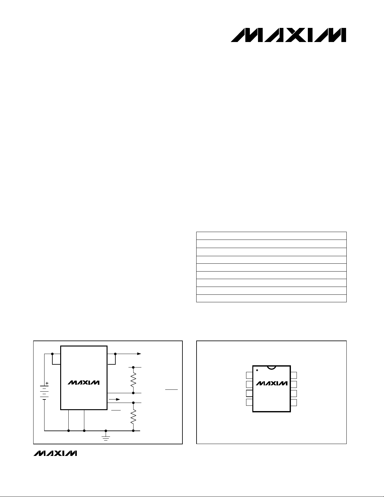
__________Typical Operating Circuit
TO
2k
I
LOAD
LOAD or CHARGER
LOGIC
SUPPLY
DISCHARGE/CHARGE
(1V/A)
V
OUT
RS+ RSRS+
3V
TO
36V
MAX471
GNDSHDN
RS-
SIGN
OUT
I
LOAD
2000
100k
_________________Pin Configurations
TOP VIEW
SHDN
RS+
RS+
1
2
MAX471
3
4
DIP/SO
8
OUT
7
RS-
6
RS-
5
SIGNGND
MAX472 Pin Configuration continued on last page.
________________________________________________________________
For free samples & the latest literature: http://www.maxim-ic.com, or phone 1-800-998-8800
Maxim Integrated Products
1
Page 2
Precision, High-Side
Current-Sense Amplifiers
ABSOLUTE MAXIMUM RATINGS
Supply Voltage, RS+, RS-, VCCto GND....................-0.3V, +40V
RMS Current, RS+ to RS- (MAX471 only)..........................±3.3A
Peak Current, (RS+ to RS-) ......................................see Figure 5
Differential Input Voltage, RG1 to RG2 (MAX472 only) .....±0.3V
Voltage at Any Pin Except SIGN
MAX471 only...........................................-0.3V to (RS+ - 0.3V)
MAX472 only ..........................................-0.3V to (V
CC
+ 0.3V)
Voltage at SIGN......................................................-0.3V to +40V
Current into SHDN, GND, OUT, RG1, RG2, V
................±50mA
CC
Current into SIGN.................................................+10mA, -50mA
Note 1: Due to special packaging considerations, MAX471 (DIP, SO) has a higher power dissipation rating than the MAX472. RS+
and RS- must be soldered to large copper traces to achieve this dissipation rating.
MAX471/MAX472
Stresses beyond those listed under “Absolute Maximum Ratings” may cause permanent damage to the device. These are stress ratings only, and functional
operation of the device at these or any other conditions beyond those indicated in the operational sections of the specifications is not implied. Exposure to
absolute maximum rating conditions for extended periods may affect device reliability.
ELECTRICAL CHARACTERISTICS—MAX471
(RS+ = +3V to +36V, TA= T
Supply Voltage
Supply Current
Sense Current
Sense Resistor
Current-Sense Ratio
No-Load OUT Error
Low-Level OUT Error
SIGN Threshold (I
LOAD
to switch SIGN)
SIGN Sink Current
Shutdown Supply Current
SHDN Input Low Voltage
SHDN Input Low Current
SHDN Input High Voltage
SHDN Input High Current
OUT Output Voltage Range
OUT Output Resistance R
OUT Rise, Fall Time tR, t
OUT Settling Time to 1%
of Final Value
MIN
required
to T
, unless otherwise noted. Typical values are at TA= +25°C.)
MAX
RS+
I
= 0A, excludes I
/
LOAD
I
= 1A,
LOAD
RS+ = 10V
I
= 0A,
LOAD
RS+
LOAD
SENSE
I
OUT
I
LOAD
RS+ = 10V
I
= 30mA,
LOAD
RS+ = 10V
3V ≤ RS+ ≤ 36V, I
MAX471C
MAX471E
OL
RS+(SHDN)
IL
IL
IH
IH
OUT
OUTILOAD
F
t
s
V
V
V
V
V
I
C
I
C
36V
SIGN =
= 0.3V
SIGN
= 2.4V; VCC= 3V to 20V
SHDN
= 0V
SHDN
= 2.4V
SHDN
= 3.0A, V
= 50mA to 3.0A, R
LOAD
= 50pF, 10% to 90%
OUT
= 100mA to 3.0A, R
LOAD
= 50pF
OUT
Continuous Power Dissipation (T
= +70°C)
A
MAX471 (Note 1):
Plastic DIP (derate 17.5mW/°C above +70°C) ..................1.4W
SO (derate 9.9mW/°C above +70°C).............................791mW
MAX472 :
Plastic DIP (derate 9.09mW/°C above +70°C) ..............727mW
SO (derate 5.88mW/°C above +70°C)...........................471mW
Operating Temperature Ranges
MAX47_C_A........................................................0°C to +70°C
MAX47_E_A.....................................................-40°C to +85°C
Junction Temperature Range............................-60°C to +150°C
Storage Temperature Range.............................-60°C to +160°C
Lead Temperature (soldering, 10sec).............................+300°C
CONDITIONS
336V
SIGN
50 113I
±3I
0.490 0.500 0.510
0.4875 0.500 0.5125
2.5
3.0
±2.5
±3.0
LOAD
MAX471C
MAX471E
MAX471C
MAX471E
MAX471C
MAX471E
= 1A
±4.0 ±6.0
±7.0
- 1.5V
RS+
OUT
= 0V to (V
OUT
OUT
- 1.5V) 13 MΩ
RS+
= 2kΩ,
= 2kΩ,
4 µs
15 µs
UNITSMIN TYP MAXSYMBOLPARAMETER
A
mA/A
V
µA
RMS
mΩ35 70R
µA
µA
%/V0.1PSRRPower-Supply Rejection Ratio
mA
µA1.0SIGN Output Leakage Current
mA0.1I
µA1.5 18.0I
V0.3V
µA1.0I
V2.4V
µA1.0I
V0V
2 _______________________________________________________________________________________
Page 3
Precision, High-Side
Current-Sense Amplifiers
ELECTRICAL CHARACTERISTICS—MAX472
(VCC= +3V to +36V, RG1 = RG2 = 200Ω, TA= T
Supply Voltage
Supply Current
Input Offset Voltage
(Note 2)
Input Bias Current
Input Bias-Current Matching
OUT Current Accuracy
V
RG1
IRG/I
CC
CC
OS
, I
OS
RG2
OUT
No-Load OUT Error
Low-Level OUT Error
SIGN Threshold (V
SENSE
required to switch SIGN)
Shutdown Supply Current
SHDN Input Low Voltage
SHDN Input Low Current
SHDN Input High Voltage
SHDN Input High Current
OUT Output Voltage Range
OUT Output Resistance R
OUT Rise, Fall Time tR, t
OUT Settling Time to 1%
of Final Value
Maximum Output Current I
CC(SHDN)
IL
IL
IH
IH
OUT
OUTIOUT
F
t
s
OUT
to T
MIN
, unless otherwise noted. Typical values are at TA = +25°C.)
MAX
CONDITIONS
I
= 0A, excludes I
LOAD
MAX472C
MAX472E
I
- I
RG1
GR2
V
SENSE
= 100mV,
VCC= 10V (Note 3)
VCC= 10V,
V
SENSE
= 0V
VCC= 10V,
V
SENSE
= 3mV
3V ≤ VCC≤ 36V, V
VCC= 10V
V
= 36V
SIGN
V
= 0.3V
SIGN
V
= 2.4V; VCC= 3V to 20V
SHDN
V
= 0V
SHDN
V
= 2.4V
SHDN
= 1.5mA 13 MΩ
V
C
V
C
= 5mV to 150mV, R
SENSE
= 50pF, 10% to 90%
OUT
= 5mV to 150mV, R
SENSE
= 50pF
OUT
; VCC= 3V to 20V
SIGN
MAX472C
MAX472E ±2.5
MAX472C
MAX472E
MAX472C
MAX472E
= 100mV
SENSE
MAX472C
MAX472E
= 2kΩ,
OUT
= 2kΩ,
OUT
1.5 mA
UNITSMIN TYP MAXSYMBOLPARAMETER
µA20 48I
120
140
µV
µA20 35I
µA±0.4 ±3.0I
±2
2.5
3
±2.5
±3.0
µA
µA
%/V0.1PSRRPower-Supply Rejection Ratio
60 120
60 140
µV
µA1.0SIGN Output Leakage Current
mA0.1SIGN Output Sink Current
µA1.5 18.0I
µA1.0I
µA1.0I
- 1.5V
CC
4 µs
15 µs
MAX471/MAX472
V336V
%
V0.3V
V2.4V
V0V
Note 2: VOSis defined as the input voltage (V
Note 3: V
is the voltage across the sense resistor.
SENSE
_______________________________________________________________________________________ 3
) required to give minimum I
SENSE
OUT
.
Page 4
Precision, High-Side
Current-Sense Amplifiers
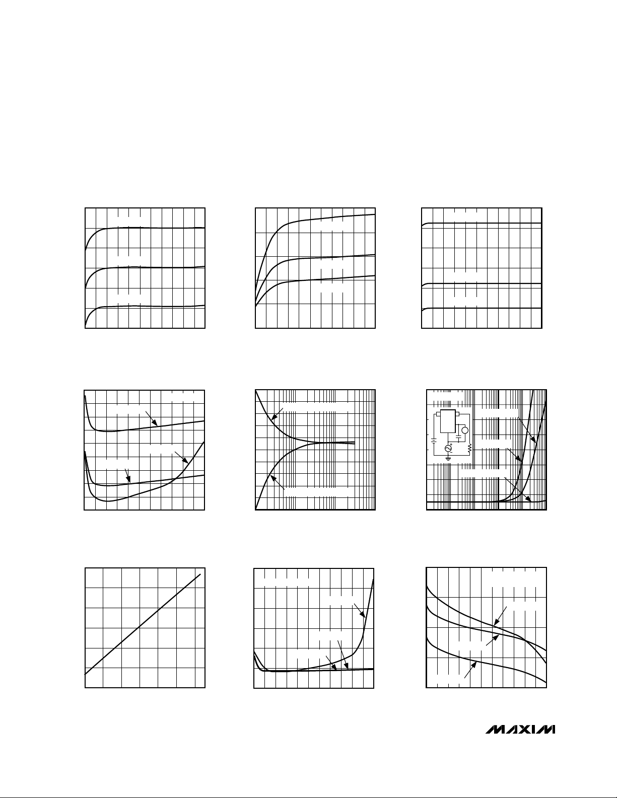
__________________________________________Typical Operating Characteristics
(Typical Operating Circuit (MAX471) or circuit of Figure 4, RG1 = RG2 = 200Ω, R
otherwise noted.)
= 2kΩ (MAX472), TA= +25°C, unless
OUT
SUPPLY CURRENT vs.
SUPPLY VOLTAGE
65
60
55
50
45
SUPPLY CURRENT (µA)
MAX471/MAX472
40
35
TA = +85°C
TA = +25°C
TA = -40°C
V
21 2415 189123 6 27 30 33 36
(V)
RS+
MAX1471-01
MAX471
NO-LOAD OFFSET CURRENT vs.
SUPPLY VOLTAGE
2.4
2.2
2.0
1.8
1.6
1.4
1.2
OFFSET CURRENT (µA)
1.0
0.8
0.6
TA = -40°C
TA = +25°C
V
RS+
VS+ = VS-
MAX1471-04
TA = +85°C
21 2415 189123 6 27 30 33 36
(V)
MAX471
RS+ TO RS- RESISTANCE vs.
TEMPERATURE
40
38
36
MAX1471-07
2.5
2.0
1.5
(µA)
SHDN
I
1.0
0.5
0
15
12
9
6
3
0
ERROR (%)
-3
-6
-9
-12
-15
0.01 0.10
3.0
2.5
2.0
SHUTDOWN CURRENT vs.
SUPPLY VOLTAGE
TA = -40°C
TA = +25°C
TA = +85°C
21 2415 189123 6 27 30 33 36
V
(V)
RS+
MAX471
ERROR vs. LOAD CURRENT
I
FROM RS- TO RS+
LOAD
I
FROM RS+ TO RS-
LOAD
I
110
(A)
LOAD
MAX472
NO-LOAD OUTPUT ERROR vs.
SUPPLY VOLTAGE
RG1 = RG2 = 0Ω
TA = +85°C
4
MAX1471-02
MAX471-05
MAX1471-08
3
2
1
0
SIGN THRESHOLD (mA)
-1
-2
40
35
30
25
20
PSRR (%)
15
10
1.10
1.00
SIGN THRESHOLD vs.
SUPPLY VOLTAGE
TA = -40°C
TA = +25°C
TA = +85°C
21 2415 189123 6 27 30 33 36
V
(V)
RS+
MAX471
POWER-SUPPLY REJECTION RATIO
vs. FREQUENCY
I
= 1A
LOAD
RS+
RS–
V = 0V TO 0.5V
OUT
A
GND
5V
1µF
V = 0V TO 1V
5Ω
V
V = 0mV TO 50mV
5
0
0.01 10 1000
POWER-SUPPLY FREQUENCY (kHz)
0.10
1 100
MAX472
ERROR vs. SUPPLY VOLTAGE
V
= 60mV,
RG1-VRG2
RG1 = RG2 = 200Ω
TA = +85°C
MAX1471-03
MAX471-06
MAX1471-09
34
32
RESISTANCE (mΩ)
30
28
-40 80
-20 0 60
20
TEMPERATURE (°C)
40
(µA)
I
OUT
1.5
1.0
0.5
TA = +25°C
TA = -40°C
0
21 2415 189123 6 27 30 33 36
VCC (V)
0.90
ERROR (%)
0.80
0.70
TA = +25°C
TA = -40°C
4 _______________________________________________________________________________________
21 2415 189123 6 27 30 33 36
V
(V)
CC
Page 5
Precision, High-Side
Current-Sense Amplifiers
____________________________Typical Operating Characteristics (continued)
(Typical Operating Circuit (MAX471) or circuit of Figure 4, RG1 = RG2 = 200Ω, R
otherwise noted.)
MAX472
25
15
ERROR (%)
-5
-15
-25
ERROR vs. SENSE VOLTAGE
V
RG1-VRG2
5
0
V
RG2-VRG1
0.1 10 1000
1 100
V
(mV)
SENSE
MAX471-10
MAX471
0mA to 100mA TRANSIENT RESPONSE
0A
100µs/div
V
= 10V, R
CC
= 2kΩ 1%, SIGN PULL-UP = 50kΩ 1%
OUT
LOAD
CURRENT
50mA/div
V
OUT
50mV/div
0A
= 2kΩ (MAX472), TA= +25°C, unless
OUT
MAX471
NOISE vs. LOAD CURRENT
0.5
0.4
)
RMS
0.3
0.2
NOISE (µA
OUT
I
0.1
0
1mA
10mA
100mA
I
SENSE
1A
MAX471
-100mA to +100mA TRANSIENT RESPONSE
V
CC
= 10V, R
OUT
50mA/div50mA/div
100µs/div
= 2kΩ 1%, SIGN PULL-UP = 50kΩ 1%
MAX471-15
LOAD
CURRENT
100mA/div
V
OUT
50mV/div
SIGN
50mV/div
MAX471/MAX472
MAX471
START-UP DELAY
10µs/div
I
= 1A, R
LOAD
= 2kΩ 1%
OUT
V
OUT
500mV/div
V
SHDN
5V/div
0A TO 3A TRANSIENT RESPONSE
R
= 2kΩ 1%
OUT
_______________________________________________________________________________________
MAX471
10µs/div
I
LOAD
1A/div
V
OUT
10mV/div
5
Page 6

Precision, High-Side
Current-Sense Amplifiers
______________________________________________________________Pin Description
PIN
MAX471
MAX471/MAX472
—
MAX472
1
—
2
3
4
5
—
6
7
8
NAME
SHDN1
RS+2, 3
SIGN5
RS-6, 7
CC
OUT8
Shutdown. Connect to ground for normal operation. When high, supply current is
less than 5µA.
Battery (or power) side of the internal current-sense resistor. The “+” indicates direction of
flow for SIGN output only. Connect pins 2 and 3 together at the package.
No Connect—no internal connectionN.C.—
Gain Resistor. Connect to battery side of current-sense resistor through the gain resistor.RG1—
Ground or Battery Negative TerminalGND4
An open-collector logic output. For the MAX471, a low level indicates current is flowing from
RS- to RS+. For the MAX472, a low level indicates a negative V
high impedance when SHDN is high. Leave open if SIGN is not needed.
Load side of the internal current-sense resistor. The “-” indicates direction of flow for SIGN
output only. Connect pins 6 and 7 together at the package.
Gain Resistor. Connect to load side of current-sense resistor through the gain resistor.RG2—
Power input for MAX472. Connect to sense resistor (R
Current output that is proportional to the magnitude of the sensed current flowing through
R
. A 2kΩ resistor from this pin to ground will result in a voltage equal to 1V/Amp of
SENSE
sensed current in the MAX471.
_______________Detailed Description
The MAX471 and MAX472 current-sense amplifier’s
unique topology allows a simple design to accurately
monitor current flow. The MAX471/MAX472 contain two
amplifiers operating as shown in Figures 1 and 2. The
battery/load current flows from RS+ to RS- (or vice
versa) through R
RG1 and Q1 or RG2 and Q2, depending on the senseresistor current direction. Internal circuitry, not shown in
Figures 1 and 2, prevents Q1 and Q2 from turning on at
the same time. The MAX472 is identical to the
MAX471, except that R
RG1 and RG2 are external (Figure 2).
To analyze the circuit of Figure 1, assume that current
flows from RS+ to RS- and that OUT is connected to
GND through a resistor. In this case, amplifier A1 is
active and output current I
Q1. Since no current flows through RG2 (Q2 is off), the
negative input of A1 is equal to V
R
). The open-loop gain of A1 forces its positive
SENSE
input to essentially the same level as the negative input.
Therefore, the drop across RG1 equals I
R
. Then, since I
SENSE
(ignoring the extremely low base currents), I
= I
LOAD
x R
SENSE
. Current flows through either
SENSE
and gain-setting resistors
SENSE
flows from the emitter of
OUT
SOURCE
flows through Q1 and RG
OUT
, or:
- (I
OUT
LOAD
LOAD
x RG1
FUNCTION
(see Figure 2). SIGN is
SENSE
) junction with RG1.V
SENSE
I
OUT
= (I
LOAD
x R
SENSE
) / RG1
Current Output
The output voltage equation for the MAX471/MAX472 is
given below. In the MAX471, the current-gain ratio has
been preset to 500µA/A so that an output resistor
(R
) of 2kΩ yields 1V/A for a full-scale value of +3V
OUT
at ±3A. Other full-scale voltages can be set with different R
greater than V
for the MAX472.
where V
I
LOAD
the current-sense resistor, R
resistor, and RG = the gain-setting resistor (RG = RG1
= RG2).
The above equation can be modified to determine the
R
x
x
OUT
For the MAX471, this reduces to:
OUT is a high-impedance current-source output that
can be connected to other MAX471/MAX472 OUT pins
values, but the output voltage can be no
OUT
V
OUT
OUT
- 1.5V for the MAX471 or V
RS+
= (R
SENSE
x R
OUT
x I
LOAD
= the desired full-scale output voltage,
= the full-scale current being sensed, R
= the voltage-setting
OUT
required for a particular full-scale range:
R
R
OUT
OUT
= (V
= V
OUT
OUT
x RG) / (I
/ (I
LOAD
x R
LOAD
x 500µA/A)
RG_
) / RG
SENSE
- 1.5V
SENSE
)
=
6 _______________________________________________________________________________________
Page 7
RS+
2, 3
Precision, High-Side
Current-Sense Amplifiers
R
SENSE
RG2RG1
6, 7
RS-
MAX471/MAX472
Q1
MAX471
Figure 1. MAX471 Functional Diagram
OR
BATTERY
A1
R
SENSE
V
SENSE
36
A2
Q2
8
OUT
5
COMP
RG2RG1
SIGN
TO LOAD/CHARGERPOWER SOURCE
Q1
MAX472
Figure 2. MAX472 Functional Diagram
_______________________________________________________________________________________ 7
A1
A2
7
V
Q2
COMP
CC
8
OUT
5
SIGN
Page 8

Precision, High-Side
Current-Sense Amplifiers
RS+ RSRS+
MAX471
3V
TO
36V
MAX471/MAX472
RS+ RSRS+
MAX471
GND
GND
RS-
SIGN
OUT
RS-
SIGN
OUT
1k
LOGIC
SUPPLY
100k
TO LOAD/
CHARGER
V
OUT
POWER
SOURCE
OR
BATTERY
3V
TO
36V
R
SENSE
RG1
SHDN
N.C.
RG1
GND
MAX472
1
2
3
4
OUT
V
RG2
SIGN
RG2
CC
TO LOAD/CHARGER
8
7
6
5
LOGIC
SUPPLY
100k
R
OUT
Figure 3. Paralleling MAX471s to Sense Higher Load Current Figure 4. MAX472 Standard Application Circuit
for current summing. A single scaling resistor is
required when summing OUT currents from multiple
devices (Figure 3). Current can be integrated by connecting OUT to a capacitive load.
SIGN Output
When SHDN is high, the MAX471/MAX472 are shut
down and consume less than 18µA. In shutdown mode,
SIGN is high impedance and OUT turns off.
__________Applications Information
The current at OUT indicates magnitude. The SIGN output indicates the current’s direction. Operation of the
SIGN comparator is straightforward. When Q1 (Figures
1 and 2) conducts, the output of A1 is high while A2’s
output is zero. Under this condition, a high SIGN output
indicates positive current flow (from RS+ to RS-). In battery-operated systems, this is useful for determining
whether the battery is charging or discharging. The
SIGN output may not correctly indicate if the load current is such that I
is less than 3.5µA. The MAX471’s
OUT
SIGN output accurately indicates the direction of current flow for load currents greater than 7mA.
SIGN is an open-collector output (sinks current only),
allowing easy interface with logic circuits powered from
any voltage. Connect a 100kΩ pull-up resistor from
SIGN to the logic supply. The convention chosen for
the polarity of the SIGN output ensures that it draws no
current when the battery is being discharged. If current
The MAX471 obtains its power from the RS- pin. This
includes MAX471 current consumption in the total system current measured by the MAX471. The small drop
across R
SENSE
does not affect the MAX471’s perfor-
mance.
Resistor Selection
Since OUT delivers a current, an external voltage gainsetting resistor (R
pin in order to get a voltage. R
to ground) is required at the OUT
OUT
SENSE
is internal to the
MAX471. RG1 and RG2 are factory trimmed for an output current ratio (output current to load current) of
500µA/A. Since they are manufactured of the same
material and in very close proximity on the chip, they
provide a high degree of temperature stability. Choose
R
for the desired full-scale output voltage up to RS-
OUT
- 1.5V (see the
Current Output
section).
direction is not needed, float the SIGN pin.
Shutdown
MAX471
8 _______________________________________________________________________________________
Page 9

Precision, High-Side
Current-Sense Amplifiers
Peak Sense Current
The MAX471’s maximum sense current is 3A
RMS
. For
power-up, fault conditions, or other infrequent events,
larger peak currents are allowed, provided they are
short— that is, within a safe operating region, as shown
in Figure 5.
50
45
TA = +25°C
40
35
30
25
20
15
SENSE CURRENT (A)
10
5
0
10µ
PULSE WIDTH (sec)
DIP safe
operating region
Figure 5. MAX471 Pulse Current Safe Operation for 10,000
Pulses and Fuse Time for Continuous Current. Pulse tests done
with 250mW average power dissipation.
Small
DIP
Outline
fuse
fuse
time
time
100µ 1m 10m
Small Outline safe
operating region
MAX472
R
the MAX472. VCCcan be connected to either the
load/charge or power-source/battery side of the sense
resistor. Connect VCCto the load/charge side of
R
in the measured current.
, RG1, and RG2 are externally connected on
SENSE
if you want to include the MAX472 current drain
SENSE
Suggested Component Values
for Various Applications
The general circuit of Figure 4 is useful in a wide variety
of applications. It can be used for high-current applications (greater than 3A), and also for those where the fullscale load current is less than the 3A of the MAX471.
Table 1 shows suggested component values and indicates the resulting scale factors for various applications
required to sense currents from 100mA to 10A.
Higher or lower sense-current circuits can also be built.
Select components and calculate circuit errors using
the guidelines and formulas in the following section.
R
Choose R
based on the following criteria:
SENSE
a) Voltage Loss: A high R
SENSE
value will cause the
SENSE
power-source voltage to degrade through IR loss.
For least voltage loss, use the lowest R
b) Accuracy: A high R
SENSE
value allows lower
SENSE
value.
currents to be measured more accurately. This is
because offsets become less significant when the
sense voltage is larger.
c) Efficiency and Power Dissipation: At high current
levels, the I2R losses in R
may be significant.
SENSE
Take this into consideration when choosing the
resistor value and power dissipation (wattage) rating. Also, if the sense resistor is allowed to heat up
excessively, its value may drift.
d) Inductance: If there is a large high-frequency com-
ponent to I
, you will want to keep inductance
SENSE
low. Wire-wound resistors have the highest inductance, while metal film is somewhat better. Lowinductance metal-film resistors are available. Instead
of being spiral wrapped around a core, as in metalfilm or wire-wound resistors, these are a straight
band of metal. They are made in values under 1Ω.
e) Cost: If the cost of R
becomes an issue, you
SENSE
may want to use an alternative solution, as shown in
Figure 6. This solution uses the PC board traces to
create a sense resistor. Because of the inaccuracies
of the copper “resistor,” you will need to adjust the
full-scale current value with a potentiometer. Also,
the resistance temperature coefficient of copper is
fairly high (approximately 0.4%/°C), so systems that
experience a wide temperature variance should take
this into account.
MAX471/MAX472
Table 1. Suggested Component Values for the MAX472
FULL-SCALE
LOAD
CURRENT,
I
(A)
SENSE
0.1 500 200 10 2.5 25
1 50 200 10 2.5 2.5
5 10 100 5 2.5 0.5
10 5 50 2 2 0.2
CURRENT-
SENSE
RESISTOR,
R
SENSE
(mΩ)
_______________________________________________________________________________________ 9
GAIN-SETTING
RESISTORS,
RG1 = RG2
(Ω)
OUTPUT
RESISTOR,
R
OUT
(kΩ)
FULL-SCALE
OUTPUT
VOLTAGE,
V
(V)
OUT
SCALE
FACTOR,
V
OUT/ISENSE
(V/A)
TYPICAL ERROR AT X%
OF FULL LOAD (%)
1% 100%10%
14 2.5
14 2.5
13 2.0
12 2.0
0.9
0.9
1.1
1.6
Page 10
Precision, High-Side
Current-Sense Amplifiers
In Figure 6, assume the load current to be measured is
10A and that you have determined a 0.3 inch wide, 2
ounce copper to be appropriate. The resistivity of 0.1
inch wide, 2 ounce copper is 30mΩ/ft (see Note 4). For
10A you may want R
SENSE
= 5mΩ for a 50mV drop at
full scale. This resistor will require about 2 inches of 0.1
inch wide copper trace.
RG1 and RG2
Once R
to define the current-gain ratio (R
is chosen, RG1 and RG2 can be chosen
SENSE
SENSE
/RG). Choose
RG = RG1 = RG2 based on the following criteria:
a) 1Ω Input Resistance. The minimum RG value is lim-
ited by the 1Ω input resistance, and also by the output current limitation (see below). As RG is reduced,
the input resistance becomes a larger portion of the
MAX471/MAX472
total gain-setting resistance. With RG = 50Ω, the
input resistance produces a 2% difference between
the expected and actual current-gain ratio. This is a
gain error that does not affect linearity and can be
removed by adjusting RG or R
b) Efficiency. As RG is reduced, I
given load current. Power dissipated in R
.
OUT
gets larger for a
OUT
OUT
going to the load, and therefore reduces overall efficiency. This is significant only when the sense current is small.
c) Maximum Output Current Limitation. I
ed to 1.5mA, requiring RG ≥ V
V
= 60mV, RG must be ≥ 40Ω.
SENSE
SENSE
OUT
/ 1.5mA. For
d) Headroom. The MAX472 requires a minimum of
1.5V between the lower of the voltage at RG1 or
RG2 (V
RG_
) and V
. As RG becomes larger, the
OUT
voltage drop across RG also becomes larger for a
given I
mum full-scale V
R
SENSE
of R
. This voltage drop further limits the maxi-
OUT
. Assuming the drop across
OUT
is small and VCCis connected to either side
SENSE
, V
(max) = VCC- (1.5V + I
OUT
OUT
RG).
e) Output Offset Error at Low Load Currents. Large
RG values reduce I
I
gets smaller, the 2.5µA max output offset-error
OUT
for a given load current. As
OUT
current becomes a larger part of the overall output
current. Keeping the gain high by choosing a low
value for RG minimizes this offset error.
f) Input Bias Current and Input Bias Current
Mismatching. The size of RG also affects the errors
introduced by the input bias and input bias mismatching currents. After selecting the ratio, check to
is not
is limit-
(max) x
V
RG2
CC
TO LOAD/CHARGER
RG2RG1
8
7
6
5
and IOSdo
B
1.5k
1k
R
SENSE
0.1" COPPER0.3" COPPER 0.3" COPPER
POWER
SOURCE
OR
BATTERY
Figure 6. MAX472 Connections Showing Use of PC Board
Trace
3V
TO
36V
SHDN
N.C.
RG1
GND
MAX472
1
2
3
4
OUT
SIGN
make sure RG is small enough that I
not add any appreciable errors. The full-scale error
is given by:
% Error =
(RG1 - RG2) x IB+ IOSx RG
IFSx R
SENSE
x 100
where RG1 and RG2 are the gain resistors, IBis the
bias current, IOSis the bias-current mismatch, IFSis the
full-scale current, and R
Assuming a 5A load current, 10mΩ R
is the sense resistor.
SENSE
SENSE
, and 100Ω
RG, the current-gain ratio is 100µA/A, yielding a fullscale I
of 500µA. Using the maximum values for I
OUT
(20µA) and IOS(2µA), and 1% resistors for RG1 and
RG2 (RG1 - RG2 = 2Ω), the worst-case error at full
scale calculates to:
2Ω x 20µA + 100Ω x 2µA
= 0.48%
5mΩ x 5A
The error may be reduced by: a) better matching of
RG1 and RG2, b) increasing R
, or c) decreasing
SENSE
RG.
Current-Sense Adjustment
(Resistor Range, Output Adjust)
Choose R
Choose R
after selecting R
OUT
to obtain the full-scale voltage you
OUT
, RG1, and RG2.
SENSE
B
Note 4: Printed Circuit Design, by Gerald L. Ginsberg; McGraw-Hill, Inc.; page 185.
10 ______________________________________________________________________________________
Page 11

Precision, High-Side
Current-Sense Amplifiers
require, given the full-scale I
R
permits using R
error. Values above 10kΩ are not usually recommended. The impedance of OUT’s load (e.g., the input of an
op amp or ADC) must be much greater than R
(e.g., 100 x R
ment accuracy.
The MAX472 can achieve higher current measurements
than the MAX471 can. Low-value sense resistors may
be paralleled to obtain even lower values, or the PC
board trace may be adjusted for any value.
An alternative method is to connect several MAX471s in
parallel and connect the high-impedance currentsource OUT pins together to indicate the total system
current (Figure 3). Pay attention to layout to ensure
equal IR drops in the paralleled connection. This is
necessary to achieve equal current sharing.
, RG1, and RG2. The high compliance of OUT
SENSE
OUT
values up to 10kΩ with minimal
OUT
) to avoid degrading the measure-
High-Current Measurement
determined by
OUT
OUT
Power-Supply Bypassing and Grounding
The MAX471 has been designed as a “high side” (positive terminal) current monitor to ease the task of
grounding any battery charger, thermistor, etc. that
may be a part of the battery pack. Grounding the
MAX471 requires no special precautions; follow the
same cautionary steps that apply to the system as a
whole. High-current systems can experience large voltage drops across a ground plane, and this drop may
add to or subtract from V
surement accuracy, use a single-point “star” ground.
. For highest current-mea-
OUT
The MAX471/MAX472 require no special bypassing,
and respond quickly to transient changes in line current. If the noise at OUT caused by these transients is a
problem, you may want to place a 1µF capacitor at the
OUT pin to ground. You can also place a large capacitor at the RS- terminal (or “load” side of the MAX472) to
decouple the load and, thereby, reduce the current
transients. These capacitors are not required for
MAX471/MAX472 operation or stability, and their use
will not degrade performance.
For the MAX472, the RG1 and RG2 inputs can be filtered by placing a capacitor (e.g., 1µF) between them
to average the sensed current.
MAX471 Layout
The MAX471 must be soldered in place, since sockets
can cause uneven current sharing between the RS+
pins (pins 2 and 3) and the RS- pins (pins 6 and 7),
resulting in typical errors of 0.5%.
In order to dissipate sense-resistor heat from large
sense currents, solder the RS+ pins and the RS- pins to
large copper traces. Keep the part away from other
heat-generating devices. This procedure will ensure
continuous power dissipation rating.
MAX471/MAX472
______________________________________________________________________________________ 11
Page 12
Precision, High-Side
Current-Sense Amplifiers
____Pin Configurations (continued)
1
SHDN
N.C.
RG1
2
MAX472
3
4
DIP/SO
8
OUT
7
V
CC
RG2
6
SIGNGND
5
MAX471/MAX472
Maxim cannot assume responsibility for use of any circuitry other than circuitry entirely embodied in a Maxim product. No circuit patent licenses are
implied. Maxim reserves the right to change the circuitry and specifications without notice at any time.
12
__________________Maxim Integrated Products, 120 San Gabriel Drive, Sunnyvale, CA 94086 (408) 737-7600
© 1996 Maxim Integrated Products Printed USA is a registered trademark of Maxim Integrated Products.
 Loading...