

Page 1
General Description
The MAX4706/MAX4707 single-pole/single-throw
(SPST) switches operate from a single 1.8V to 5.5V supply. The MAX4706 is a normally closed (NC) switch and
the MAX4707 is the normally open (NO) version. These
switches provide 2Ω on-resistance (RON) and 0.6Ω
RONflatness with a +2.7V supply. These devices typically consume only 0.02µA of quiescent current, making them suitable for use in low-power, portable
applications. The MAX4706/MAX4707 feature low-leakage currents over the entire temperature range,
TTL/CMOS-compatible digital logic, and excellent AC
characteristics.
The MAX4706/MAX4707 are offered in small 5-pin and
6-pin SC70 and 6-pin µDFN packages.
Applications
Battery-Operated Equipment
Audio Signal Routing
Low-Voltage Data-Acquisition Systems
Sample-and-Hold Circuits
Communications Circuits
Relay Replacement
Features
♦ Guaranteed R
ON
2Ω max (+2.7V Supply)
♦ Guaranteed RONFlatness: 0.6Ω (+2.7V Supply)
♦ Excellent AC Characteristics
High Off-Isolation: -67dB at 1MHz
-3dB Bandwidth: 190MHz
♦ 0.013% Total Harmonic Distortion
♦ Low Supply Current: 0.02µA
♦ Tiny SC70 and µDFN Packages
♦ 1.8V to 5.5V Single-Supply Operation
MAX4706/MAX4707
Low-Voltage, 2Ω, SPST,
CMOS Analog Switches
________________________________________________________________ Maxim Integrated Products 1
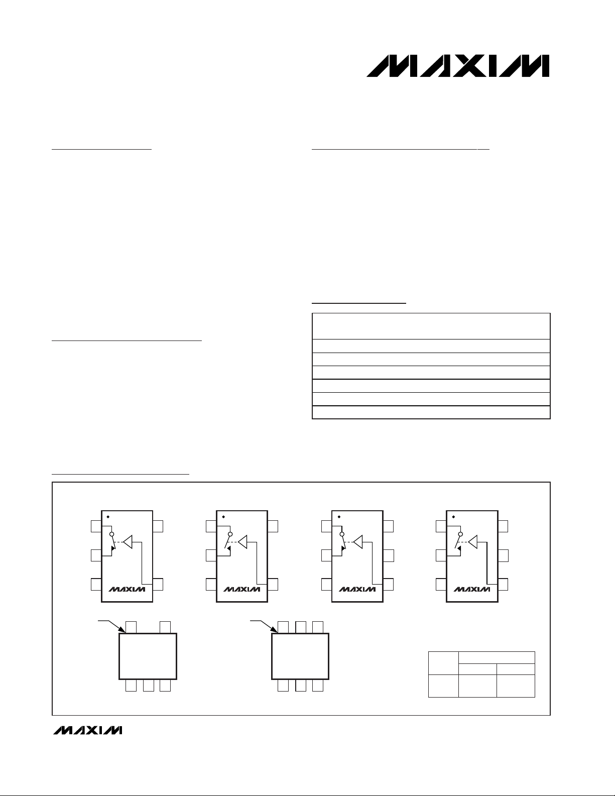
NC
INGND
15V+COM
MAX4706
SC70-5
TOP VIEW
2
3
4
NO
INGND
15V+COM
MAX4707
SC70-5
2
34
NC
INGND
16V+
5 N.C. N.C.5
COM
MAX4706
SC70-6
2
34
NO
INGND
16V+COM
MAX4707
SC70-6
2
34
N.C. = NOT INTERNALLY CONNECTED.
SWITCHES SHOWN FOR LOGIC 0 INPUT.
INPUT
0
1
SWITCH STATE
MAX4706
ON
OFF
MAX4707
ON
OFF
PIN 6
6
XYZ
4
NOTE: SC70-6
PACK AGE
HAS LETTERING
NEAREST PIN 6.
5
123
PIN 5
5
XYZ
4
NOTE: SC70-5
PACKAGE
HAS LETTERING
NEAREST PIN 5.
123
Pin Configurations/Functional Diagrams/Truth Tables
Ordering Information
19-3159; Rev 0; 1/04
For pricing, delivery, and ordering information, please contact Maxim/Dallas Direct! at
1-888-629-4642, or visit Maxim’s website at www.maxim-ic.com.
PART
TEMP RANGE
PIN-
TOP
MARK
MAX4706EXK-T
5 SC70-5 AFO
MAX4706EXT-T
6 SC70-6 ABS
MAX4706ELT-T*
6 µDFN-6 —
MAX4707EXK-T
5 SC70-5 AFP
MAX4707EXT-T
6 SC70-6 ABT
MAX4707ELT-T*
6 µDFN-6 —
Pin Configurations/Functional Diagrams/Truth Tables continued at end of data sheet.
*Future product—contact factory for availability.
PACKAGE
-40°C to +85°C
-40°C to +85°C
-40°C to +85°C
-40°C to +85°C
-40°C to +85°C
-40°C to +85°C
Page 2
MAX4706/MAX4707
Low-Voltage, 2Ω, SPST,
CMOS Analog Switches
2 _______________________________________________________________________________________
ABSOLUTE MAXIMUM RATINGS
ELECTRICAL CHARACTERISTICS
(V+ = 2.7V to 3.6V, VIH= 2.0V, VIL= 0.4V, TA= T
MIN
to T
MAX
, unless otherwise noted. Typical values are at TA= +25°C.) (Note 2)
Stresses beyond those listed under “Absolute Maximum Ratings” may cause permanent damage to the device. These are stress ratings only, and functional
operation of the device at these or any other conditions beyond those indicated in the operational sections of the specifications is not implied. Exposure to
absolute maximum rating conditions for extended periods may affect device reliability.
(All voltages referenced to ground.)
V+, IN .......................................................................-0.3V to +6V
COM, NO, NC (Note 1).................................-0.3V to (V+ + 0.3V)
Continuous Current (IN, V+, GND) ...................................
±30mA
Continuous Current COM, NO, NC.................................±160mA
Peak Current COM, NO, NC
(pulsed at 1ms, 10% duty cycle) ................................±300mA
Continuous Power Dissipation (T
A
= +70ºC)
5-Pin SC70 (derate 3.1mW/ºC above +70ºC) ..............247mW
6-Pin SC70 (derate 3.1mW/ºC above +70ºC) ..............245mW
6-Pin µDFN (derate 2.1mW/ºC above +70°C)...........167.7mW
Operating Temperature Range ...........................-40°C to +85°C
Storage Temperature Range .............................-65°C to +150°C
Lead Temperature (soldering, 10s) .................................+300°C
Junction Temperature......................................................+150°C
PARAMETER
SYMBOL
CONDITIONS
MIN
TYP
MAX
UNITS
ANALOG SWITCH
Analog Signal Range
V
COM
,
0V+V
TA = +25°C
3.0
On-Resistance R
ON
V+ = 2.7V, I
COM
= 10mA,
V
NO
or VNC = 0V to V+
3.5
Ω
TA = +25°C
On-Resistance Flatness
(Note 3)
)
V+ = 2.7V, I
COM
= 10mA,
V
NO
or VNC = 0V to V+
Ω
TA = +25°C -1
+1
NO, NC Off-Leakage
Current
I
NO(OFF),
)
V+ = 3.3V, V
COM
= 1V, 3V;
V
NO
or VNC = 3V, 1V
-2 +2
nA
TA = +25°C -1
+1
)
V+ = 3.3V, V
COM
= 1V or 3V;
-2 +2
nA
TA = +25°C -1
+1
COM Off-Leakage Current
)
V+ = 3.3V, V
COM
= 1V or 3V;
V
NO
or V
NC
= 3V, 1V
-2 +2
nA
DIGITAL INPUTS
Input Logic High V
IH
V
Input Logic Low V
IL
0.4 V
Input Current I
IN
VIN = 0V or V+ -1
+1 µA
DYNAMIC
TA = +25°C 12 20
Turn-On Time (Note 4) t
ON
V
COM
= 2V, RL = 300Ω,
C
L
= 35pF, Figure 2
20
ns
TA = +25°C 8 15
Turn-Off Time (Note 4) t
OFF
V
COM
= 2V, RL = 300Ω,
C
L
= 35pF, Figure 2
15
ns
Charge Injection Q V
GEN
= 0V, R
GEN
= 0, CL = 1.0nF, Figure 3 5 pC
NO, NC Off-Capacitance
C
NO(OFF)
,
)
VNO, V
NC
= GND, f = 1MHz, Figure 5 17 pF
Switch On-Capacitance C
ON
V
COM
= V
NO/NC
, f = 1MHz, Figure 5 35 pF
Note 1: Signals on NO, NC, COM, or IN exceeding V+ or GND are clamped by internal diodes. Limit forward-diode current to maxi-
mum current rating.
V
NO, VNC
R
FLAT (ON
COM On-Leakage Current I
I
NC(OFF
COM(ON
I
COM(OFF
C
NC(OFF
TA = T
TA = T
TA = T
MIN
MIN
MIN
to T
to T
to T
MAX
MAX
MAX
VNO or V
= 1V, 3V, or floating
NC
T
= T
A
TA = T
MIN
MIN
to T
to T
MAX
MAX
2.0
TA = T
TA = T
MIN
MIN
to T
MAX
to T
MAX
2.0
0.6 0.85
0.1
0.1
0.1
0.05
0.97
Page 3
MAX4706/MAX4707
Low-Voltage, 2Ω, SPST,
CMOS Analog Switches
_______________________________________________________________________________________ 3
ELECTRICAL CHARACTERISTICS (continued)
(V+ = 2.7V to 3.6V, VIH= 2.0V, VIL= 0.4V, TA= T
MIN
to T
MAX
, unless otherwise noted. Typical values are at TA= +25°C.) (Note 2)
Note 2: SC70 and µDFN packaged parts are 100% tested at +25°C. Limits across the full temperature range are guaranteed by
design and correlation.
Note 3: R
ON
flatness is defined as the difference between the maximum and minimum value of on-resistance as measured over the
specified analog signal ranges.
Note 4: Guaranteed by design.
Note 5: Off-isolation = 20log10 (VO / VI), where VO is V
COM
and VI is either VNCor VNOfrom the network analyzer.
PARAMETER
SYMBOL
CONDITIONS
MIN
TYP
MAX
UNITS
f = 10MHz
Off-Isolation (Note 5) V
ISO
VNO = VNC = 1V
RMS,
RL = 50Ω, CL = 5pF, Figure 4
f = 1MHz
dB
On-Channel Bandwidth
-3dB
BW R
L
= 50Ω, CL = 5pF, Figure 4
MHz
Total Harmonic Distortion THD
TA = +25°C
%
SUPPLY
TA = +25°C
Positive Supply Current I+ V+ = 5.5V, VIN = 0V or V+
1
µA
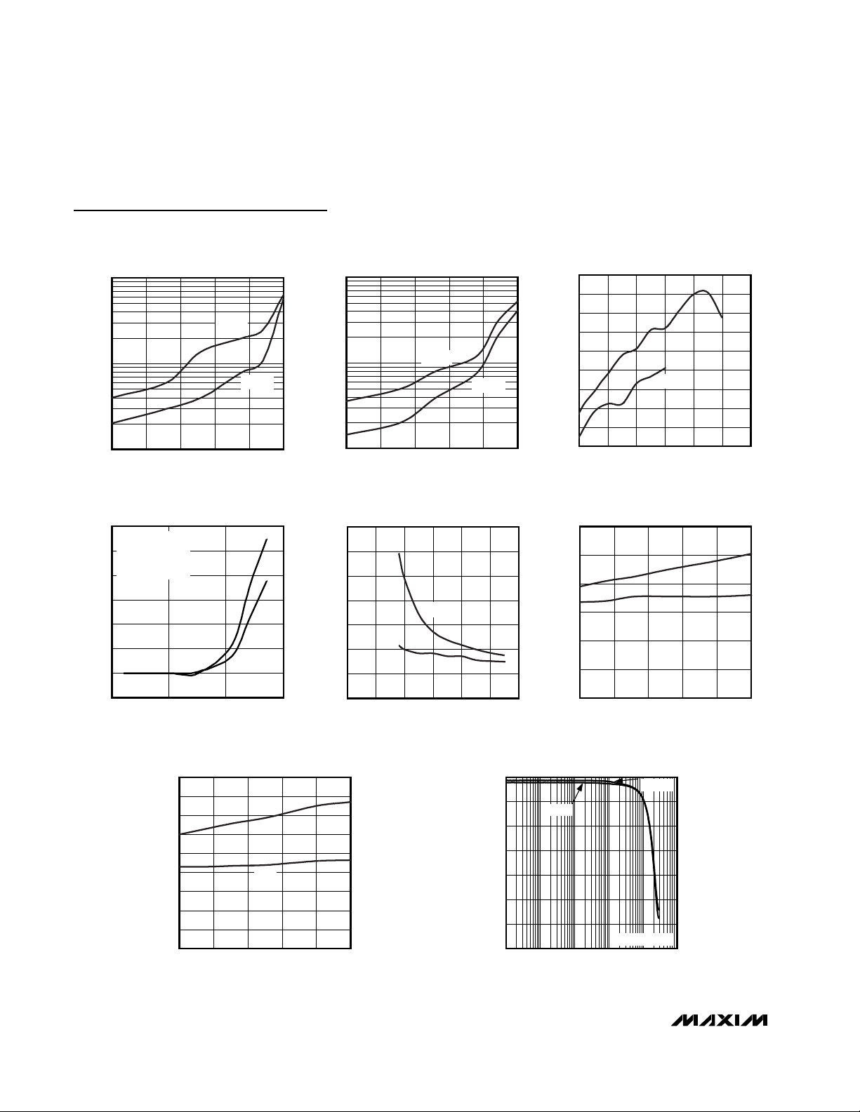
Typical Operating Characteristics
(TA = +25°C, unless otherwise noted.)
ON-RESISTANCE vs. V
COM
MAX4706 toc01
V
COM
(V)
ON-RESISTANCE (Ω)
54321
1
2
3
4
5
6
7
0
06
V+ = 1.8V
V+ = 2.5V
V+ = 3V
V+ = 4.5V
V+ = 5V
ON-RESISTANCE vs. V
COM
MAX4706 toc02
V
COM
(V)
ON-RESISTANCE (Ω)
541 2 3
0.2
0.4
0.6
0.8
1.0
1.2
1.4
1.6
0
06
TA = +85°C
T
A
= +25°C
T
A
= -40°C
V+ = 5V
ON-RESISTANCE vs. V
COM
MAX4706 toc03
V
COM
(V)
ON-RESISTANCE (Ω)
321
0.5
1.0
1.5
2.0
2.5
0
04
TA = +85°C
T
A
= +25°C
T
A
= -40°C
V+ = 3V
RL = 600Ω, 2V
-62
-82
190
, f = 20H z to 20kH z
P - P
0.013
0.02
TA = T
MIN
to T
MAX
Page 4
MAX4706/MAX4707
Low-Voltage, 2Ω, SPST,
CMOS Analog Switches
4 _______________________________________________________________________________________
Typical Operating Characteristics (continued)
(TA = +25°C, unless otherwise noted.)
ON-LEAKAGE CURRENT
vs. TEMPERATURE
MAX4706 toc04
TEMPERATURE (°C)
ON-LEAKAGE CURRENT (nA)
-15 10 35 60
0.10
1.00
0.01
-40 85
V+ = 5V
V+ = 3V
OFF-LEAKAGE CURRENT
vs. TEMPERATURE
MAX4706 toc05
TEMPERATURE (°C)
OFF-LEAKAGE CURRENT (nA)
-15 10 35 60
0.10
1.00
0.01
-40 85
V+ = 5V
V+ = 3V
CHARGE INJECTION vs. V
COM
MAX4607 toc06
V
C0M
(V)
CHARGE INJECTION (pC)
54321
5
10
15
20
25
30
35
40
45
0
06
5V
3V
SUPPLY CURRENT vs. TEMPERATURE
MAX4706 toc07
TEMPERATURE (°C)
SUPPLY CURRENT (nA)
0
0.50
1.00
1.50
2.00
2.50
3.00
-0.50
V+ = 5V
V+ = 3V
500-50 100
VIN = V+;
ALL OTHER SWITCH
TERMINALS ARE
FLOATING
tON/t
OFF
vs. SUPPLY VOLTAGE
MAX4706 toc08
SUPPLY VOLTAGE (V)
t
ON
/t
OFF
(ns)
54321
5
10
15
20
25
30
35
0
06
t
ON
t
OFF
tON/t
OFF
vs. TEMPERATURE
MAX4706 toc09
TEMPERATURE (°C)
t
ON
/t
OFF
(ns)
603510-15
2
4
6
8
10
12
0
-40 85
t
ON
V+ = 5V
t
OFF
tON/t
OFF
vs. TEMPERATURE
MAX4706 toc10
TEMPERATURE (°C)
t
ON
/t
OFF
(ns)
603510-15
2
4
6
8
10
12
14
16
18
0
-40 85
t
ON
V+ = 3V
t
OFF
ON-LOSS BANDWIDTH
MAX4706 toc11
FREQUENCY (MHz)
RESPONSE (dB)
1001010.1
-6
-5
-4
-3
-2
-1
0
-7
0.01 1000
V+ = 5V
V+ = 3V
50Ω IN AND OUT
Page 5

MAX4706/MAX4707
Low-Voltage, 2Ω, SPST,
CMOS Analog Switches
_______________________________________________________________________________________ 5
OFF-ISOLATION
MAX4706 toc12
FREQUENCY (MHz)
RESPONSE (dB)
100101
-80
-70
-60
-50
-40
-30
-20
-10
0
-90
0.1 1000
50Ω IN AND OUT
V+ = 3V
V+ = 5V
Pin Description
PIN
MAX4706 MAX4707
NAME FUNCTION
116116COM Analog Switch Common Terminal
222——— NC Analog Switch Normally Closed Terminal
331331GND Ground
443443 IN Logic Input Control
564564V+ Positive Supply Voltage
———2 22NO Analog Switch Normally Open Terminal
—5 5—5 5N.C. No Connection. Not internally connected.
Typical Operating Characteristics (continued)
(TA = +25°C, unless otherwise noted.)
TOTAL HARMONIC DISTORTION
vs. FREQUENCY
MAX4706 toc13
FREQUENCY (kHz)
THD (%)
1010.1
0.002
0.004
0.006
0.008
0.010
0.012
0.014
0.016
0.018
0.020
0
0.01 100
INPUT IMPEDANCE = 600Ω
f = 20Hz TO 20kHz
V+ = 3V, V
GEN
= 3V
P-P
V+ = 3V, V
GEN
= 2V
P-P
V+ = 5V, V
GEN
= 5V
P-P
V+ = 5V, V
GEN
= 3V
P-P
SC70-5 SC70-6 µDFN-6 SC70-5 SC70-6 µDFN-6
Page 6

Detailed Description
The MAX4706/MAX4707 SPST switches operate from a
single supply ranging from 1.8V to 5.5V. The MAX4706
is a normally closed (NC) switch and the MAX4707 is
the normally open (NO) version. These switches provide
3.5Ω on-resistance (RON) and 0.9Ω RONflatness with a
+2.7V supply. These devices typically consume only
0.02µA of quiescent current, making them suitable for
use in low-power, portable applications. The
MAX4706/MAX4707 feature low-leakage currents over
the entire temperature range, TTL/CMOS-compatible
digital logic, and excellent AC characteristics.
The MAX4706/MAX4707 are offered in small 5-pin and
6-pin SC70 and 6-pin µDFN packages.
Applications Information
The MAX4706/MAX4707 operate from a single +1.8V to
+5.5V supply. The MAX4706/MAX4707 accept bipolar
input signals when V+ and GND are biased from bipolar
supplies. For example, the switch accepts a 1V
P-P
input
when V+ = 2V and GND = -2V. ESD-protection diodes
are internally connected between each analog switch
terminal and both V+ and GND. One of these diodes
conducts if any analog signal is greater than V+ or less
than GND (Figure 1). Virtually all analog leakage current
is attributed to the ESD diodes. Each diode is biased by
the analog signal and either V+ or GND. The ESD
diodes’ leakage currents vary as the signal changes.
Power-Supply Sequencing and
Overvoltage Protection
Caution: Do not exceed the absolute maximum
ratings because stresses beyond the listed ratings
may cause permanent damage to the device.
Proper power-supply sequencing is recommended for
all CMOS devices. Always apply V+ before applying
analog signals, especially if the analog signal is not
current-limited.
MAX4706/MAX4707
Low-Voltage, 2Ω, SPST,
CMOS Analog Switches
6 _______________________________________________________________________________________
V+
POSITIVE SUPPLY
D1
D2
N0
V
g
GND
COM
MAX4706
MAX4707
Figure 1. Overvoltage Protection Using Two External Blocking
Diodes
tr < 5ns
tf < 5ns
50%
0V
LOGIC
INPUT
R
L
NO
OR NC
GND
C
L
INCLUDES FIXTURE AND STRAY CAPACITANCE.
V
OUT
= V
COM (
RL
)
RL + R
ON
SWITCH
INPUT
IN
V+
t
OFF
0V
COM
SWITCH
OUTPUT
0.9 x V
0UT
0.9 x V
0UT
t
ON
V
OUT
SWITCH
OUTPUT
LOGIC
INPUT
LOGIC INPUT WAVEFORMS INVERTED FOR SWITCHES
THAT HAVE THE OPPOSITE LOGIC SENSE.
V+
C
L
V+
V
OUT
V
COM
MAX4706
MAX4707
Figure 2. Switching Time
Page 7

MAX4706/MAX4707
Low-Voltage, 2Ω, SPST,
CMOS Analog Switches
_______________________________________________________________________________________ 7
V
GEN
GND
C
L
V
OUT
V+
V
OUT
∆V
OUT
Q = (∆V
OUT
)(CL)
COM
SWITCH
INPUT
ON
0V
V+
OFFOFF
IN
V+
R
GEN
IN
MAX4706
MAX4707
SWITCH
OUTPUT
LOGIC INPUT (0 TO V+)
NO
OR NC
Figure 3. Charge Injection
MEASUREMENTS ARE STANDARDIZED AGAINST
SHORT AT SOCKET TERMINALS. OFF-ISOLATION IS
MEASURED BETWEEN COM AND “OFF” TERMINAL
ON EACH SWITCH. ON-LOSS IS MEASURED BETWEEN
COM AND “ON” TERMINAL ON EACH SWITCH. SIGNAL
DIRECTION THROUGH SWITCH IS REVERSED; WORST
VALUES ARE RECORDED.
V+
V+
V
MEAS
GND
V+
IN
NO
OR
NC
COM
V
IN
MAX4706
MAX4707
OFF-ISOLATION = 20log
V
MEAS
V
REF
ON-LOSS = 20log
V
MEAS
V
REF
NETWORK
ANALYZER
50Ω
50Ω 50Ω
50Ω
MEAS REF
0.1µF
50Ω
V
REF
Figure 4. Off-Isolation and On-Loss Bandwidth
V+
GND
V+
IN
NO
OR
NC
COM
MAX4706
MAX4707
AS
REQUIRED
f = 1MHz
CAPACITANCE
ANALYZER
Figure 5. Channel Off/On-Capacitance
Chip Information
TRANSISTOR COUNT: 190
PROCESS: CMOS
Page 8

MAX4706/MAX4707
Low-Voltage, 2Ω, SPST,
CMOS Analog Switches
8 _______________________________________________________________________________________
NC
V+IN
16COM
5 N.C.
GND
MAX4706
µDFN-6
TOP VIEW
2
34
NO
V+IN
16COM
5 N.C.
GND
µDFN-6
2
34
MAX4707
N.C. = NOT INTERNALLY CONNECTED.
SWITCHES SHOWN FOR LOGIC 0 INPUT.
INPUT
0
1
SWITCH STATE
MAX4706
ON
OFF
MAX4707
ON
OFF
Pin Configurations/Functional Diagrams/Truth Tables (continued)
Page 9

MAX4706/MAX4707
Low-Voltage, 2Ω, SPST,
CMOS Analog Switches
_______________________________________________________________________________________ 9
Package Information
(The package drawing(s) in this data sheet may not reflect the most current specifications. For the latest package outline information,
go to www.maxim-ic.com/packages
.)
SC70, 5L.EPS
Page 10

MAX4706/MAX4707
Low-Voltage, 2Ω, SPST,
CMOS Analog Switches
10 ______________________________________________________________________________________
SC70, 6L.EPS
Package Information (continued)
(The package drawing(s) in this data sheet may not reflect the most current specifications. For the latest package outline information,
go to www.maxim-ic.com/packages
.)
Page 11

MAX4706/MAX4707
Low-Voltage, 2Ω, SPST,
CMOS Analog Switches
Maxim cannot assume responsibility for use of any circuitry other than circuitry entirely embodied in a Maxim product. No circuit patent licenses are
implied. Maxim reserves the right to change the circuitry and specifications without notice at any time.
Maxim Integrated Products, 120 San Gabriel Drive, Sunnyvale, CA 94086 408-737-7600 ____________________ 11
© 2004 Maxim Integrated Products Printed USA is a registered trademark of Maxim Integrated Products.
Package Information (continued)
(The package drawing(s) in this data sheet may not reflect the most current specifications. For the latest package outline information,
go to www.maxim-ic.com/packages
.)
6L UDFN.EPS
1
1
REV.DOCUMENT CONTROL NO.APPROVAL
PROPRIETARY INFORMATION
TITLE:
21-0147
B
L
TOP VIEW
D
E
SIDE VIEW
A1
PIN 1
INDEX AREA
A
A 0.64
COMMON DIMENSIONS
PIN 1
0.075x45∞
BOTTOM VIEW
L1
3
2
MIN.
1
e
6
5
b
4
SECTION A-A
b
L2
A A
NOM.
0.72 0.80
MAX.
0.20--A1 --
1.501.45D 1.55
1.000.95E 1.05
0.350.30L 0.40
----
L1
0.08
----L2 0.05
0.200.17b 0.23
0.50--
e
--
 Loading...