

Page 1
General Description
The MAX4674 is a low-voltage CMOS analog switch containing four 2:1 multiplexers/demultiplexer. When powered from a single +5V supply, it features a low 4Ω max
on-resistance (RON), 0.4Ω max RONmatching between
channels, and 0.8Ω RON flatness over the entire signal
range. Off-leakage current is only 0.5nA max at +25°C.
The MAX4674 features fast turn-on (tON) and turn-off
(t
OFF
) times of 18ns and 6ns, respectively, and is avail-
able in QFN, QSOP, TSSOP, and SO packages.
This low-voltage multiplexer operates with a +1.8V to
+5.5V single supply. All digital inputs have +0.8V and
+2.4V logic thresholds, ensuring TTL/CMOS-logic compatibility with +5V operation.
________________________Applications
10/100 Base-T
ATM Switching
Audio and Video Signal Routing
Low-Voltage Data-Acquisition Systems
Communications Circuits
Relay Replacement
Features
♦ Guaranteed On-Resistance
4Ω max (+5V Supply)
6Ω max (+3V Supply)
♦ Guaranteed Match Between Channels
0.4Ω max
♦ Guaranteed Flatness Over Signal Range
0.8Ω max
♦ 1.8V Operation
R
ON
= 100Ω typ Over Temperature
tON= 51ns typ
t
OFF
= 13ns typ
♦ Guaranteed Low Leakage Currents
0.5nA max at +25°C
♦ Single-Supply Operation from +1.8V to +5.5V
♦ Rail-to-Rail Signal Handling
♦ TTL/CMOS-Logic Compatible
♦ Crosstalk: -114dB (1MHz)
♦ Off-Isolation: -67dB (1MHz)
♦ 4mm
✕ 4mm QFN Package
MAX4674
3V/5V, 4Ω, Wideband Quad
2:1 Analog Multiplexer
________________________________________________________________ Maxim Integrated Products 1
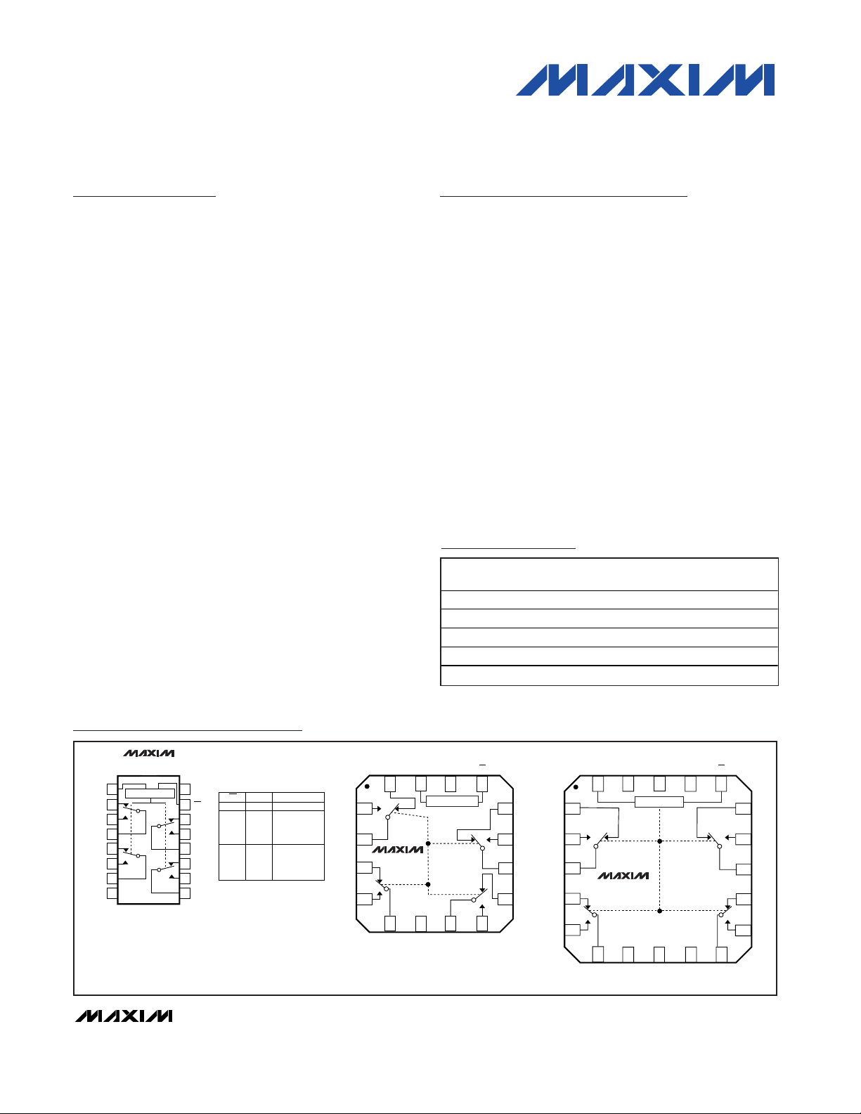
1
2
3
4
5678
9
10
11
12
13141516
NC1 A0 V+ EN
NC4
NO4
COM4
NC3
NO3COM3GND
QFN
COM2
NO2
NC2
COM1
NO1
1
2
4
5
67
910
11
13
14
15
16171920
AO N.C.
18
V+ N.C. EN
NC4
NO4
COM4
12
NC3
NO3
COM3N.C.
N.C.
8
GND
QFN
COM2
NO2
NC2
NO1
3
COM1
NC1
CONTROL LOGIC
CONTROL LOGIC
16
15
14
13
12
11
10
9
1
2
3
4
5
6
7
8
A0 V+
EN
NC4
NO4
COM4
NC3
NO3
COM3
TOP VIEW
MAX4674
MAX4674
MAX4674
QSOP/TSSOP/SO
NC1
NO1
NO2
COM1
NC2
COM2
GND
CONTROL LOGIC
EN
1
0
0
A0
X
0
1
ON SWITCH
NONE
COM1-NC1
COM2-NC2
COM3-NC3
COM4-NC4
COM1-NO1
COM2-NO2
COM3-NO3
COM4-NO4
Pin Configuration/Functional Diagram/Truth Table
19-1708; Rev 3; 12/06
Ordering Information
PA R T
T EM P
R A N G E
PIN PA C K A G E
PK G
C O D E
M AX 4674E E E
16 QS OP E 16- 4
M AX 4674E U E
16 TS S O P U 16- 2
M AX 4674E S E
S 16- 2
M AX 4674E GE
16 QFN - E P *
G 1644- 1
M AX 4674E GP
20 QFN - E P *
G 2044- 3
For pricing, delivery, and ordering information, please contact Maxim/Dallas Direct! at
1-888-629-4642, or visit Maxim’s website at www.maxim-ic.com.
*EP = Exposed pad.
- 40°C to + 85° C
- 40°C to + 85° C
- 40°C to + 85° C 16 N ar r ow S O
- 40°C to + 85° C
- 40°C to + 85° C
Page 2
MAX4674
3V/5V, 4Ω, Wideband Quad
2:1 Analog Multiplexer
2 _______________________________________________________________________________________
ABSOLUTE MAXIMUM RATINGS
ELECTRICAL CHARACTERISTICS—Single +5V Supply
(V+ = +4.5V to +5.5V, VIH= 2.4V, VIL= 0.8V, TA= T
MIN
to T
MAX
, unless otherwise noted. Typical values at TA= +25°C.) (Notes 2, 3)
Stresses beyond those listed under “Absolute Maximum Ratings” may cause permanent damage to the device. These are stress ratings only, and functional
operation of the device at these or any other conditions beyond those indicated in the operational sections of the specifications is not implied. Exposure to
absolute maximum rating conditions for extended periods may affect device reliability.
V+, A0, EN................................................................-0.3V to +6V
COM_, NO_, NC_ (Note1)...............................-0.3V to (V + 0.3V)
Continuous Current COM_, NO_, NC_ ..........................±100mA
Peak Current (COM_, NO_, NC_)
(pulsed at 1ms, 10% duty cycle) ..............................±300mA
Continuous Power Dissipation (T
A
= +70°C)
16-Pin QSOP (derate 8.3mW/°C above +70°C) ........ 667mW
16-Pin TSSOP (derate 6.7mW/°C above +70°C) .......533mW
16-Pin Narrow SO (derate 8mW/°C above +70°C) ....640mW
16-Pin QFN (derate 18.5mW/°C above +70°C) ........1481mW
20-Pin QFN (derate 20mW/°C above +70°C) ...........1600mW
Operating Temperature Range
MAX4674E_E .................................................-40°C to +85°C
Die Temperature ..............................................................+150°C
Storage Temperature Range ............................-65°C to +150°C
Lead Temperature (soldering, 10s) ................................+300°C
Note 1: Signals on NO_, NC_, and COM_ exceeding V+ or GND are clamped by internal diodes. Limit forward-diode current to max-
imum current rating.
PARAMETER
SYMBOL
CONDITIONS
MIN
TYP
MAX
UNITS
ANALOG SWITCH
Analog Signal Range
V
NC_
0V+V
TA = +25°C 2.2 4
On-Resistance R
ON
V+ = 4.5V, I
COM_
= 10mA,
V
NO_
or V
NC_
= 0 to V+
T
A
= T
MIN
to
T
MAX
5
Ω
TA = +25°C
0.4
On-Resistance Match Between
Channels (Notes 4, 5)
∆R
ON
V+ = 4.5V, I
COM_
= 10mA,
V
NO_
or V
NC_
= 0 to V+
T
A
= T
MIN
to
T
MAX
0.5
Ω
TA = +25°C 0.5 0.8
On-Resistance Flatness
(Note 6)
)
V+ = 4.5V, I
COM_
= 10mA,
V
NO_
or V
NC_
= 0 to V+
T
A
= T
MIN
to
T
MAX
1
Ω
TA = +25°C
NO_, NC_ Off-Leakage
Current (Note 7)
I
NO_(OFF),
)
V+ = 5.5V; V
COM_
= 1V,
4.5V; V
NO_
or V
NC_
= 4.5V,
1V
T
A
= T
MIN
to
T
MAX
-1 +1
nA
TA = +25°C
COM_ Off-Leakage Current
(Note 7)
)
V+ = 5.5V; V
COM_
= 1V,
4.5V; V
NO_
or V
NC_
= 4.5V,
1V
T
A
= T
MIN
to
T
MAX
-1 +1
nA
TA = +25°C
COM_ On-Leakage Current
(Note 7)
)
V+ = 5.5V; V
COM_
= 1V,
4.5V; V
NO_
or V
NC_
= 1,
4.5V, or floating
T
A
= T
MIN
to
T
MAX
-1 +1
nA
DIGITAL I/O (A0, EN)
Input Logic High V
IH
V
Input Logic Low V
IL
0.8 V
Input Leakage Current I
IN
VIN = 0 or +5.5V
±1
µA
DYNAMIC
TA = +25°C
10 18
Turn-On Time (Note 7) t
ON
V
NO_
or V
NC_
= 3V,
R
L
= 100Ω, CL = 35pF,
Figure 2
T
A
= T
MIN
to
T
MAX
20
ns
V
COM_,VNO_
R
FLAT (ON
I
NC_(OFF
I
COM_(OFF
I
COM_(ON
,
-0.5 ±0.01 +0.5
-0.5 ±0.01 +0.5
-0.5 ±0.01 +0.5
2.4
-0.5
0.15
+0.5
Page 3
MAX4674
3V/5V, 4Ω, Wideband Quad
2:1 Analog Multiplexer
_______________________________________________________________________________________ 3
ELECTRICAL CHARACTERISTICS—Single +5V Supply (continued)
(V+ = +4.5V to +5.5V, VIH= 2.4V, VIL= 0.8V, TA= T
MIN
to T
MAX
, unless otherwise noted. Typical values at TA= +25°C.) (Notes 2, 3)
ELECTRICAL CHARACTERISTICS—Single +3V Supply
(V+ = +2.7V to +3.3V, VIH= 2.0V, VIL= 0.4V, TA=T
MIN
to T
MAX
, unless otherwise noted. Typical values at TA= +25°C.) (Notes 2, 3)
PARAMETER
SYMBOL
CONDITIONS
MIN
TYP
MAX
UNITS
TA = +25°C46
Turn-Off Time (Note 7) t
OFF
V
NO_
or V
NC_
= 3V,
R
L
= 100Ω, CL = 35pF,
Figure 2
T
A
= T
MIN
to
T
MAX
8
ns
TA = +25°C5
Break-Before-Make (Note 7) t
BBM
V
NO_
or V
NC_
= 3V,
R
L
= 100Ω, CL = 35pF,
Figure 3
T
A
= T
MIN
to
T
MAX
1
ns
Charge Injection Q
V
GEN
= 4V, R
GEN
= 0, CL = 1.0nF, Figure 4
10 pC
f = 10MHz -47
Off-Isolation (Note 8) V
ISO
CL = 5pF, R
L
= 100Ω,
f = 10MHz, Figure 5
f = 1MHz -67
dB
f = 10MHz -68
Crosstalk (Note 9) V
CT
CL = 5pF, R
L
= 100Ω,
f = 10MHz, Figure 5
f = 1MHz
dB
Total Harmonic Distortion THD RL = 600Ω, f = 20Hz to 20kHz
%
NO_, NC_ Off-Capacitance
C
NO_(OFF),
)
V
NO_
, V
NC_
= GND, f = 1MHz, Figure 6 10 pF
COM_ Off-Capacitance
)
V
COM_
= GND, f = 1MHz, Figure 6 20 pF
COM_ On-Capacitance C
(ON)
30 pF
SUPPLY
Supply Range V+
5.5 V
Positive Supply Current I+ V+ = +5.5V, VIN = 0 or V+
1.0 µA
)
)
C
NC_(OFF
C
COM_(OFF
V
C OM_
= V
, V
N O_
= GN D , f = 1M Hz, Fi g ure 6
N C _
-114
0.015
1.8
0.001
PARAMETER SYMBOL CONDITIONS MIN TYP MAX UNITS
ANALOG SWITCH
Analog Signal Range
On-Resistance R
On-Resistance Match Between
Channels (Notes 4, 5)
On-Resistance Flatness
(Note 6)
NO_, NC_ Off-Leakage
Current (Note 7)
V
, VNO,
COM
V
NC_
ON
∆R
ON
R
FLAT(ON
I
NO_(OFF),
I
NC_(OFF
V+ = 2.7V, I
V
NO_
V+ = 2.7V, I
V
NO_
V+ = 2.7V, I
V
NO_
V + = 3.3V ; V
V
N O_
COM_
or V
= 0 to V+
NC_
COM_
or V
= 0 to V+
NC_
or V
or V
COM_
NC_
C OM _
N C _
= 0 to V+
= 3V , 1V
= 10mA,
= 10mA,
= 10mA,
= 1V , 3V ;
TA = +25°C46
T
= T
= T
MIN
MIN
to
to
A
T
MAX
TA = +25°C 0.15 0.4
T
A
T
MAX
TA = +25°C23
T
= T
MIN
to
T
A
MAX
TA = +25°C-0.5±0.01 +0.5
= T
MIN
to
T
T
A
MAX
0V+V
8
0.5
4
-1 +1
Ω
Ω
Ω
nA
Page 4
Note 2: The algebraic convention, where the most negative value is a minimum and the most positive value a maximum, is used in
this data sheet.
Note 3: Parts are tested at the maximum hot-rated temperature. Limits across the entire temperature range are guaranteed by
design and correlation.
Note 4: ∆R
ON
= R
ON(MAX)
- R
ON(MIN)
.
Note 5: ∆R
ON
matching specifications for QFN packaged parts are guaranteed by design.
Note 6: Flatness is defined as the difference between the maximum and minimum value of on-resistance as measured over the
specified analog signal range.
Note 7: Guaranteed by design.
Note 8: Off-Isolation = 20log
10(VCOM/VNO
), V
COM
= output, VNO= input to off switch.
Note 9: Between any two switches.
MAX4674
3V/5V, 4Ω, Wideband Quad
2:1 Analog Multiplexer
4 _______________________________________________________________________________________
ELECTRICAL CHARACTERISTICS—Single +3V Supply (continued)
(V+ = +2.7V to +3.3V, VIH= 2.0V, VIL= 0.4V, TA=T
MIN
to T
MAX
, unless otherwise noted. Typical values at TA= +25°C.) (Notes 2, 3)
PARAMETER
SYMBOL
CONDITIONS
MIN
TYP
MAX
UNITS
TA = +25°C
COM_ Off-Leakage Current
(Note 7)
)
V + = 3.3V ; V
C OM _
= 1V , 3V ;
V
N O_
or V
N C _
= 3V , 1V
T
A
= T
MIN
to
T
MAX
-1 +1
nA
TA = +25°C
COM_ On-Leakage Current
(Note 7)
)
V
NO_
or V
NC_
= 1V, 3V, or
floating
T
A
= T
MIN
to
T
MAX
-1 +1
nA
DIGITAL I/O (A0, EN)
Input Logic High V
IH
2.0 V
Input Logic Low V
IL
0.4 V
Input Leakage Current I
IN
VIN = 0 or +5.5V
±1
µA
DYNAMIC
TA = +25°C1222
Turn-On Time (Note 7) t
ON
V
NO_
or V
NC_
= 1.5V,
R
L
= 100Ω, CL = 35pF,
Figure 2
T
A
= T
MIN
to
T
MAX
25
ns
TA = +25°C58
Turn-Off Time (Note 7) t
OFF
V
NO_
or V
NC_
= 1.5V,
R
L
= 100Ω, CL = 35pF,
Figure 2
T
A
= T
MIN
to
T
MAX
10
ns
TA = +25°C5
Break-Before-Make (Note 7) t
BBM
V
NO_
or V
NC
= 1.5V,
R
L
= 100Ω, CL = 35pF,
Figure 3
T
A
= T
MIN
to
T
MAX
1
ns
Charge Injection Q
V
GEN
= 2V, R
GEN
= 0, CL = 1.0nF,
Figure 4
18 pC
f = 10MHz -47
Off-Isolation (Note 8) V
ISO
CL = 5pF, R
L
= 100Ω,
f = 10MHz, Figure 5
f = 1MHz -67
dB
f = 10MHz -68
Crosstalk (Note 9) V
CT
CL = 5pF, R
L
= 100Ω,
f = 10MHz, Figure 5
f = 1MHz
dB
NO_, NC_ Off-Capacitance
)
)
V
NO_
or V
NC_
= GND, f = 1MHz, Figure 6 10 pF
COM_ Off-Capacitance
)
V
COM_
= GND, f = 1MHz, Figure 6 20 pF
COM_ On-Capacitance C
(ON)
V
COM_
= V
NO_
, V
NC_
= GND, f = 1MHz,
Figure 6
30 pF
SUPPLY
Positive Supply Current I+ V+ = 3.3V, VIN = 0 or V+
1.0 µA
I
COM_(OFF
-0.5 ±0.01 +0.5
V + = 3.3V ; V
I
COM_(ON
C
NO_(OFF
C
NC_(OFF
C
COM_(OFF
,
C OM _
= 1V , 3V ;
-0.5 ±0.01 +0.5
-0.5
-114
0.001
+0.5
Page 5

MAX4674
3V/5V, 4Ω, Wideband Quad
2:1 Analog Multiplexer
_______________________________________________________________________________________ 5
0
6
4
2
8
10
12
021 345
ON-RESISTANCE vs. V
COM
MAX4674-01
V
COM
(V)
R
ON
(Ω)
V+ = 2.5V
V+ = 1.8V
V+ = 3.0V
V+ = 5.0V
0
1.5
1.0
0.5
2.0
2.5
3.0
021354
ON-RESISTANCE vs. V
COM
MAX4674-02
V
COM
(V)
R
ON
(Ω)
TA = +85°C
V+ = 5V
TA = +25°C
TA = -40°C
1000
0.1
-40 10-15 85
ON/OFF-LEAKAGE CURRENT
vs. TEMPERATURE
1
10
100
MAX4674-03
TEMPERATURE (°C)
I
COM
(pA)
35 60
I
ON_LEAK
I
OFF_LEAK
0
5
10
15
20
25
021 345
CHARGE INJECTION
vs. V
COM
MAX4674-04
V
COM
(V)
Q (pC)
5
15
10
25
20
35
30
40
0231 456
SUPPLY CURRENT
vs. SUPPLY VOLTAGE
MAX4674-05
V+ (V)
I+ (pA)
0
5
10
15
20
25
30
12345
TURN-ON/-OFF TIME
vs. SUPPLY VOLTAGE
MAX4674-06
V+ (V)
t
ON
/t
OFF
(ns)
t
ON
t
OFF
0
4
2
8
6
10
12
-40 20 40-20 0 60 80
TURN-ON/-OFF TIME
vs. TEMPERATURE
MAX4674-07
TEMPERATURE (°C)
t
ON
/t
OFF
(ns)
t
ON
t
OFF
-120
-80
-100
-40
-60
0
-20
20
0.01 10.1 10 100 1000
OFF-ISOLATION, ON-RESPONSE,
AND CROSSTALK vs. FREQUENCY
MAX4674-08
FREQUENCY (MHz)
AMPLITUDE (dB)
OFF-ISOLATION
ON-RESPONSE
CROSSTALK
0.020
0.002
10 1k 10k100 100k
TOTAL HARMONIC DISTORTION
vs. FREQUENCY
MAX4674-09
FREQUENCY (Hz)
THD (%)
0.004
0.008
0.006
0.012
0.010
0.014
0.018
0.016
Typical Operating Characteristics
(V+ = +5V, TA= +25°C, unless otherwise noted.)
Page 6

MAX4674
3V/5V, 4Ω, Wideband Quad
2:1 Analog Multiplexer
6 _______________________________________________________________________________________
Detailed Description
The MAX4674 is a low on-resistance (RON), low-voltage, quad 2:1 analog multiplexer/demultiplexer that
operates from a +1.8V to +5.5V single supply. The
MAX4674 features very fast switching speed (tON=
18ns max, t
OFF
= 6ns max) and guaranteed breakbefore-make switching. Its low RONallows high continuous currents to be switched in a variety of applications.
Digital Interface
A0 and EN are CMOS digital inputs that meet TTL logic
levels when V+ = 5V. Note that A0 and EN can exceed
the voltage at V+ to a maximum of +5.5V. This feature
allows operation of the MAX4674 from a +3.3V supply
while controlling it with 5V CMOS logic signals.
The Pin Configuration/Functional Diagram/Truth Table
located on the first page of this data sheet details the
operation of the MAX4674.
Applications Information
Power-Supply Considerations
Overview
The MAX4674 construction is typical of most CMOS
analog switches. It has two supply pins, V+ and GND,
used to drive the internal CMOS switches and set the
limits of the analog voltage on any switches. Reverse
ESD-protection diodes are internally connected
between each analog-signal pin and both V+ and
GND. If any analog signal exceeds V+ and GND, one
of these diodes conducts. During normal operation,
these and other reverse-biased ESD diodes leak, forming the only current drawn from VCCor GND.
Virtually all the analog leakage current comes from the
ESD diodes. Although the ESD diodes on a given signal pin are identical and therefore fairly well balanced,
they are reverse biased differently. Each is biased by
either V+ or GND and the analog signal. This means
Pin Description
PIN
20 QFN 16 QFN
FUNCTION
1 20 15 A0 Address Input
2 1 16 NC1 Normally Closed Terminal
3 2 1 NO1 Normally Open Terminal
432
Analog Switch Common Terminal
5 4 3 NC2 Normally Closed Terminal
6 5 4 NO2 Normally Open Terminal
765
Analog Switch Common Terminal
—
— N.C. No Connection
8 8 6 GND Ground
9107
Analog Switch Common Terminal
10 11 8 NO3 Normally Open Terminal
11 12 9 NC3 Normally Closed Terminal
12 13 10
Analog Switch Common Terminal
13 14 11 NO4 Normally Open Terminal
14 15 12 NC4 Normally Closed Terminal
15 16 13 EN Output Enable, Active Low
16 18 14 V+ Positive Supply Voltage
— EP EP EP Exposed Pad. Connect to GND.
QSOP/TSSOP/SO
NAME
COM1
COM2
7, 9, 17, 19
COM3
COM4
Page 7

MAX4674
3V/5V, 4Ω, Wideband Quad
2:1 Analog Multiplexer
_______________________________________________________________________________________ 7
their leakages will vary as the signal varies. The difference in the two-diode leakages to the V+ and GND
pins constitutes the analog-signal-path leakage current.
All analog leakage current flows between each pin and
one of the supply terminals, not to the other switch terminal, which is why both sides of a given switch can
show leakage currents of either the same or opposite
polarity.
V+ and GND power the internal logic and set the input
logic limits. Logic inputs have ESD-protection diodes to
ground.
The logic-level thresholds are TTL/CMOS compatible
when V+ is +5V. As V+ rises, the threshold increases;
as V+ falls, the threshold decreases. For example,
when V+ = +3V, the guaranteed minimum logic-high
threshold decreases to 2.0V.
Low-Voltage Operation
The MAX4674 operates from a single supply between
+1.8V and +5.5V. At room temperature, it actually
“works” with a single supply near or below +1.7V; as
supply voltage decreases, however, switch on-resistance becomes very high.
Overvoltage Protection
Proper power-supply sequencing is recommended for
all CMOS devices. Do not exceed the absolute maximum ratings because stresses beyond the listed rat-
ings can cause permanent damage to the device.
Always sequence V+ on first, followed by the logic
inputs and analog signals. If power-supply sequencing
is not possible, add two small signal diodes (D1, D2) in
series with the supply pins for overvoltage protection
(Figure 1).
Adding diodes reduces the analog-signal range to one
diode drop below V+ and one diode drop above GND,
but does not affect the device’s low switch resistance
and low leakage characteristics. Device operation is
unchanged, and the difference between V+ and GND
should not exceed 6V. These protection diodes are not
recommended if signal levels must extend to ground.
High-Frequency Performance
In 50Ω systems, signal response is reasonably flat up
to 50MHz (see the Typical Operating Characteristics).
Above 20MHz, the on response has several minor
peaks that are highly layout dependent. The problem is
not turning the switch on, but turning it off. The off-state
switch acts like a capacitor and passes higher frequencies with less attenuation. At 10MHz, off-isolation is
about -50dB in 50Ω systems, becoming worse (approximately 20dB per decade) as frequency increases.
Higher circuit impedances also degrade off-isolation.
Adjacent channel attenuation is about 3dB above that
of a bare IC socket and is entirely due to capacitive
coupling.
Chip Information
TRANSISTOR COUNT: 478
GND
V+
*INTERNAL PROTECTION DIODES
D2
EXTERNAL
BLOCKING DIODE
D1
EXTERNAL
BLOCKING DIODE
GND
V+
MAX4674
*
*
*
*
Figure 1. Overvoltage Protection Using External Blocking
Diodes
Page 8

MAX4674
3V/5V, 4Ω, Wideband Quad
2:1 Analog Multiplexer
8 _______________________________________________________________________________________
Test Circuits/Timing Diagrams
V
AO
V+
V
OUT
GND
V+
AO
COM
NO
V
NO_
NC
MAX4674
R
L
CL*
50Ω
*CL INCLUDES STRAY CAPACITANCE.
EN
50%
V
IH
+ 0.5V
0
V
OUT
GND
V
AO
90%
t
OFF
t
ON
tR < 5ns
t
F
< 5ns
Figure 2. Turn-On and Turn-Off Times
50%
V
IH
+ 0.5V
0
V
COM
V
OUT
V
AO
0
90%
t
BBM
V
AO
V+
V
OUT
GND
V+
AO
NC, NO
COM
V
N_ _
MAX4674
R
L
CL*
50Ω
*CL INCLUDES STRAY CAPACITANCE.
t
R
< 5ns
t
F
< 5ns
EN
Figure 3. Break-Before-Make Interval
0
V+
∆ V
OUT
IS THE MEASURED VOLTAGE DUE TO CHARGE-
TRANSFER ERROR Q WHEN THE CHANNEL TURNS OFF.
∆ V
OUT
Q = ∆ V
OUT
✕ C
L
V
OUT
V+
V
OUT
V
GEN
R
GEN
GND
V+
AO
V+ OR GND
NC, NO
COM
MAX4674
50Ω
C
L
*
EN
V
EN
*CL INCLUDES STRAY CAPACITANCE.
V
EN
Figure 4. Charge Injection
Page 9

MAX4674
3V/5V, 4Ω, Wideband Quad
2:1 Analog Multiplexer
_______________________________________________________________________________________ 9
NOTES: MEASUREMENTS ARE STANDARDIZED AGAINST SHORTS AT SOCKET TERMINALS.
OFF-ISOLATION IS MEASURED BETWEEN COM AND "OFF" NO TERMINAL ON EACH SWITCH.
ON-LOSS IS MEASURED BETWEEN COM AND "ON" NO TERMINAL ON EACH SWITCH.
CROSSTALK IS MEASURED FROM ONE CHANNEL TO ALL OTHER CHANNELS.
SIGNAL DIRECTION THROUGH SWITCH IS REVERSED; WORST VALUES ARE RECORDED.
V+
V
OUT
V
IN
GND
V+
V
IN
V
OUT
MEAS
NETWORK
ANALYZER
50Ω 50Ω
50Ω
OFF-ISOLATION = 20log
ON-LOSS = 20log
CROSSTALK = 20log
50Ω
REF
V
OUT
V
IN
V
OUT
V
IN
AO
V+ OR GND
NC, NO
COM
10nF
MAX4674
EN
Figure 5. Off-Isolation, On-Loss, and Crosstalk
V+
GND
V+
AO
V+ OR GND
1MHz
CAPACITANCE
ANALYZER
NC, NO
COM
MAX4674
EN
Figure 6. Capacitance
Test Circuits/Timing Diagrams (continued)
Page 10

MAX4674
3V/5V, 4Ω, Wideband Quad
2:1 Analog Multiplexer
10 ______________________________________________________________________________________
QSOP.EPS
F
1
1
21-0055
PACKAGE OUTLINE, QSOP .150", .025" LEAD PITCH
TSSOP4.40mm.EPS
PACKAGE OUTLINE, TSSOP 4.40mm BODY
21-0066
1
1
I
Package Information
(The package drawing(s) in this data sheet may not reflect the most current specifications. For the latest package outline information,
go to www.maxim-ic.com/packages
.)
Page 11

MAX4674
3V/5V, 4Ω, Wideband Quad
2:1 Analog Multiplexer
______________________________________________________________________________________ 11
SOICN .EPS
PACKAGE OUTLINE, .150" SOIC
1
1
21-0041
B
REV.DOCUMENT CONTROL NO.APPROVAL
PROPRIETARY INFORMATION
TITLE:
TOP VIEW
FRONT VIEW
MAX
0.010
0.069
0.019
0.157
0.010
INCHES
0.150
0.007
E
C
DIM
0.014
0.004
B
A1
MIN
0.053A
0.19
3.80 4.00
0.25
MILLIMETERS
0.10
0.35
1.35
MIN
0.49
0.25
MAX
1.75
0.050
0.016L
0.40 1.27
0.3940.386D
D
MINDIM
D
INCHES
MAX
9.80 10.00
MILLIMETERS
MIN
MAX
16
AC
0.337 0.344 AB8.758.55 14
0.189 0.197 AA5.004.80 8
N MS012
N
SIDE VIEW
H 0.2440.228 5.80 6.20
e 0.050 BSC 1.27 BSC
C
HE
e
B
A1
A
D
0-8
L
1
VARIATIONS:
Package Information (continued)
(The package drawing(s) in this data sheet may not reflect the most current specifications. For the latest package outline information,
go to www.maxim-ic.com/packages
.)
Page 12

MAX4674
3V/5V, 4Ω, Wideband Quad
2:1 Analog Multiplexer
12 ______________________________________________________________________________________
12,16,20, 24L QFN.EPS
E
1
2
21-0106
PACKAGE OUTLINE
12,16,20,24L QFN, 4x4x0.90 MM
E
2
2
21-0106
PACKAGE OUTLINE
12,16,20,24L QFN, 4x4x0.90 MM
Package Information (continued)
(The package drawing(s) in this data sheet may not reflect the most current specifications. For the latest package outline information,
go to www.maxim-ic.com/packages
.)
Page 13

3V/5V, 4Ω, Wideband Quad
2:1 Analog Multiplexer
Maxim cannot assume responsibility for use of any circuitry other than circuitry entirely embodied in a Maxim product. No circuit patent licenses are
implied. Maxim reserves the right to change the circuitry and specifications without notice at any time.
Maxim Integrated Products, 120 San Gabriel Drive, Sunnyvale, CA 94086 408-737-7600 ____________________ 13
© 2006 Maxim Integrated Products is a registered trademark of Maxim Integrated Products, Inc.
MAX4674
12,16,20, 24L QFN.EPS
E
1
2
21-0106
PACKAGE OUTLINE
12,16,20,24L QFN, 4x4x0.90 MM
E
2
2
21-0106
PACKAGE OUTLINE
12,16,20,24L QFN, 4x4x0.90 MM
Revision History
Pages changed at Rev 3: 1–7, 10–13
Package Information (continued)
(The package drawing(s) in this data sheet may not reflect the most current specifications. For the latest package outline information,
go to www.maxim-ic.com/packages
.)
 Loading...