

Page 1
19-0258; Rev 2; 4/95
EVALUATION KIT MANUAL
FOLLOWS DATA SHEET
8x4 Video Crosspoint Switches with Buffers
_______________General Description
The MAX458/MAX459 are crosspoint switches with eight
input channels and four high-speed, buffered output
channels. The MAX458 output buffer is configured with a
gain of one, while the MAX459 buffer has a gain of two. In
each device, any one of eight input lines can be connected to any of four output amplifiers. The output buffers are
capable of driving loads of 75Ω.
Data interface can be accomplished by either a 16-bit
serial or a 6-bit parallel connection. In the serial mode,
the MAX458/MAX459 are SPITM, QSPITM, and Microwire
compatible. In parallel mode, the MAX458/MAX459 are
compatible with most microprocessor buses. Three-state
amplifier output capability makes it possible to multiplex
MAX458/MAX459s to form larger switch networks. The
output buffers can be disabled individually or the entire
device can be shut down to conserve power.
________________________Applications
Video Test Equipment
Video Security Systems
____________________________Features
♦ 100MHz Unity-Gain Bandwidth
♦ 300V/µs Slew Rate
♦ Low 0.05° Differential Phase Error
♦ Low 0.01% Differential Gain Error
♦ Directly Drives 75Ω Cables
♦ Fast 60ns Switching Time
♦ High-Z Amplifier Output Capability
♦ Shutdown Capability
♦ 16-Bit Serial and 6-Bit Parallel Address Modes
TM
♦ 40-Pin DIP and 44-Pin PLCC Packages
______________Ordering Information
PART
MAX458CPL
MAX458CQH
MAX458EPL -40°C to +85°C
MAX459CPL
MAX459CQH
MAX459EPL -40°C to +85°C
TEMP. RANGE PIN-PACKAGE
0°C to +70°C
0°C to +70°C
0°C to +70°C 40 Plastic DIP
0°C to +70°C
Video Editing
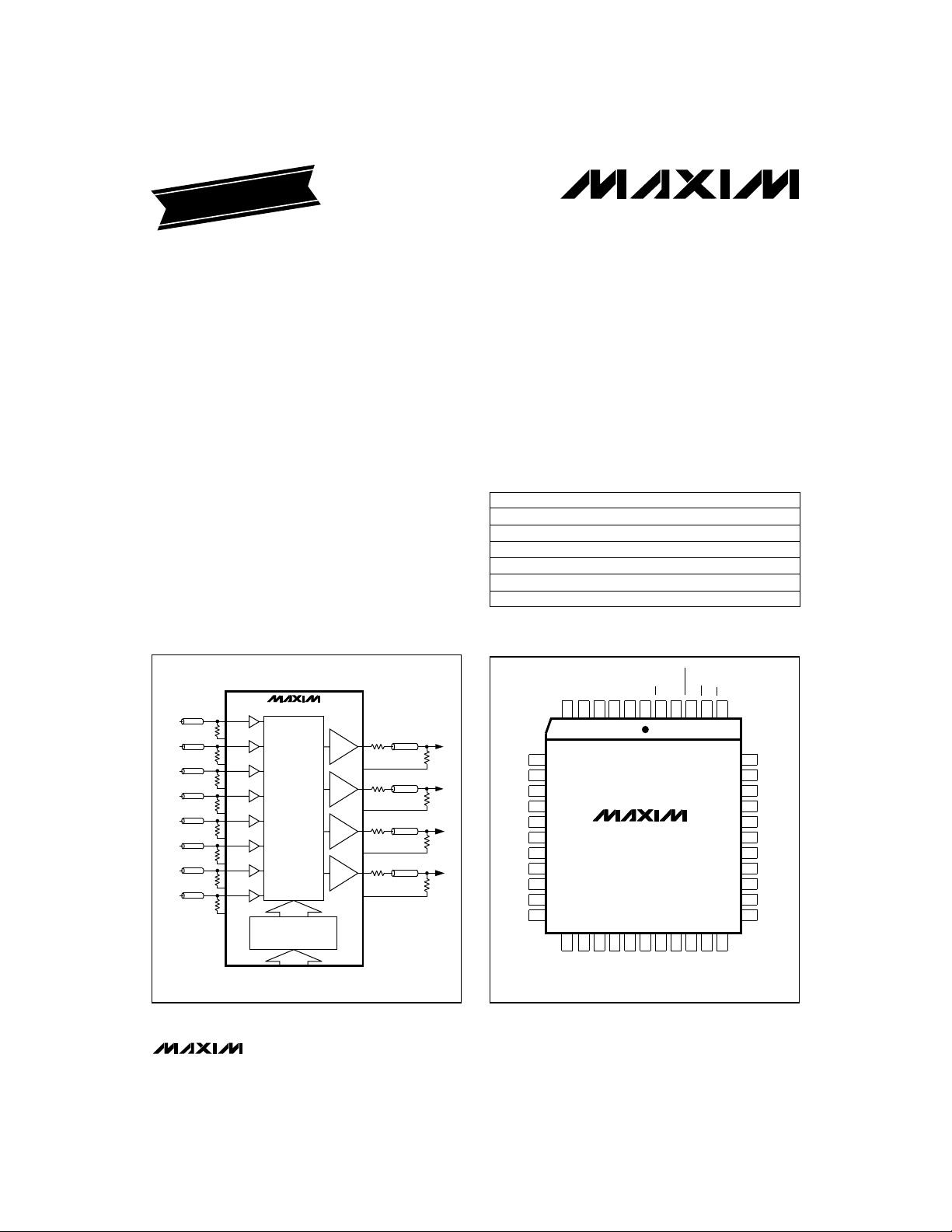
_____________________Block Diagram
8 BUFFERED
INPUTS
IN0
75Ω
IN1
IN2
IN3
IN4
IN5
IN6
IN7
™
SPI and QSPI are trademarks of Motorola, Inc. Microwire is a trademark of National Semiconductor Corp.
GND
75Ω
GND
75Ω
GND
75Ω
GND
75Ω
GND
75Ω
GND
75Ω
GND
75Ω
GND
(SPI™, QSPI™, MICROWIRE™ COMPATIBLE)
8 x 4
SWITCH ARRAY
SERIAL OR PARALLEL
DIGITAL INTERFACE
SERIAL/PARALLEL INTERFACE
MAX459
8 x 4
SWITCH
ARRAY
& CONTROL
OUTPUT DRIVERS
AV = 2
AV = 2
AV = 2
AV = 2
4 75Ω
GND
GND
GND
GND
75Ω
75Ω
75Ω
75Ω
OUT0
75Ω
OUT1
75Ω
OUT2
75Ω
OUT3
75Ω
_________________Pin Configurations
TOP VIEW
GND
IN0
GND
N.C.
MAX458
MAX459
21
22 2319
20
IN7
GND
DOUT
SHDN
PLCC
IN1
7
GND
8
IN2
9
10
GND
11
IN3
12
V
CC
13
IN4
14
V
EE
15
IN5
GND
16
IN6
17
DIP on last page.
N.C.
5
6
18
GND
40 Plastic DIP
44 PLCC
40 Plastic DIP
44 PLCC
40 Plastic DIP
DINCSSCLK
UPDATEWRCE
43
441234404142
25
26
24
D3D1D2A1D0
27
N.C.
MAX458/MAX459
39
GND
38
OUT0
37
GND
36
OUT1
35
V
CC
34
OUT2
33
V
EE
32
N.C.
31
OUT3
30
GND
29
A0
28
_______________________________________________________________
Maxim Integrated Products
Call toll free 1-800-998-8800 for free samples or literature.
1
Page 2
8x4 Video Crosspoint Switches with Buffers
ABSOLUTE MAXIMUM RATINGS
Total Supply Voltage (VCCto VEE).........................................12V
Positive Supply Voltage (VCCto GND).....................................6V
Negative Supply Voltage (VEEto GND)...................................6V
Analog Input/Output Voltage ...........(VCC+ 0.3V) to (VEE- 0.3V)
Digital Input Voltage...................................(VCC+ 0.3V) to -0.3V
Duration of Output Short Circuit to GND (Note 1)......Continuous
Continuous Power Dissipation
Plastic DIP (derate 17mW/°C above +70°C) ..............1333mW
PLCC (derate 13mW/°C above +70°C) ......................1067mW
Note 1: Outputs may be shorted to any supply pin or ground as long as package power dissipation ratings are not exceeded.
Stresses beyond those listed under “Absolute Maximum Ratings” may cause permanent damage to the device. These are stress ratings only, and functional
operation of the device at these or any other conditions beyond those indicated in the operational sections of the specifications is not implied. Exposure to
absolute maximum rating conditions for extended periods may affect device reliability.
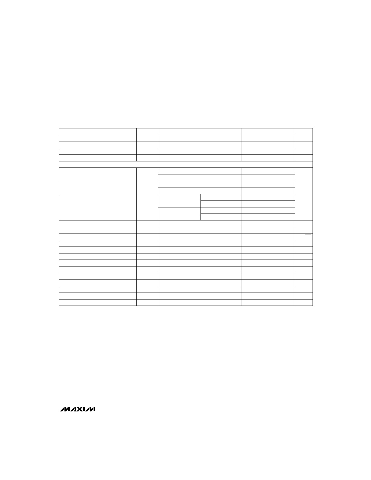
ELECTRICAL CHARACTERISTICS
(VCC= +5V, VEE= -5V, -2V ≤ VIN≤ +2V, output load resistor (RL) = 150Ω, TA= T
MAX458/MAX459
Typical values are at T
STATIC SPECIFICATIONS
Input Offset Voltage
Input Offset Voltage Match
On Input Bias Current
On Input Resistance
Input Capacitance
DC Voltage Gain Accuracy
Output Voltage Swing
Enabled Output Resistance
Disabled Output Resistance
Disabled Output Capacitance
Positive Power-Supply Current
Negative Power-Supply Current
Positive Supply Current in
Shutdown
Negative Supply Current in
Shutdown
Logic Input High Voltage
Logic Input Low Voltage
= +25°C.)
A
V
OS
OS
IN
IN
IN
OUT
R
OUT
R
OUT
OUT
I
CC
I
EE
IH
IL
Any channel
VIN= 0V (Note 2)
VS= ±4.75V to ±5.25V dB50 60PSRRPower-Supply Rejection Ratio
VIN= 0V, input programmed to one output
Input programmed to one output
Input channel on or off
MAX458 (Note 3)
MAX459 (Note 4)
VIN= 1kHz sine wave
VIN= 10MHz sine wave
MAX458
MAX459
VIN= 0V,
all amplifiers enabled
VIN= 0V,
all amplifiers enabled
(Note 5)
(Note 5)
Operating Temperature Ranges
MAX45_C_ _ ........................................................0°C to +70°C
MAX45_E_ _......................................................-40°C to +85°C
Junction Temperature......................................................+150°C
Storage Temperature Range.............................-65°C to +160°C
Lead Temperature (soldering, 10sec).............................+300°C
to T
MIN
, unless otherwise noted.
MAX
CONDITIONS
TA= +25°C
TA= T
MIN
TA= +25°C
TA= T
MIN
TA= +25°C
TA= T
MIN
to T
to T
to T
MAX
MAX
MAX
515
20
0.1 0.5
1.0
0.1 1.0
2.0
0.05
4.0
0.70 1.0
TA= +25°C
TA= T
MIN
TA= +25°C
TA= T
MIN
to T
to T
MAX
MAX
60 75 85
50 100
50 65 75
40 90
UNITSMIN TYP MAXSYMBOLPARAMETER
V-2 +2Input Voltage Range
mV
mV310∆V
µA±1 ±5I
MΩ0.50 5.0R
pF7C
%
V±2 ±3V
Ω
MΩ0.25 1.0
kΩ
pF12C
mA
mA
mA15 26
mA712
V2.0V
V0.8V
2 _______________________________________________________________________________________
Page 3
8x4 Video Crosspoint Switches with Buffers
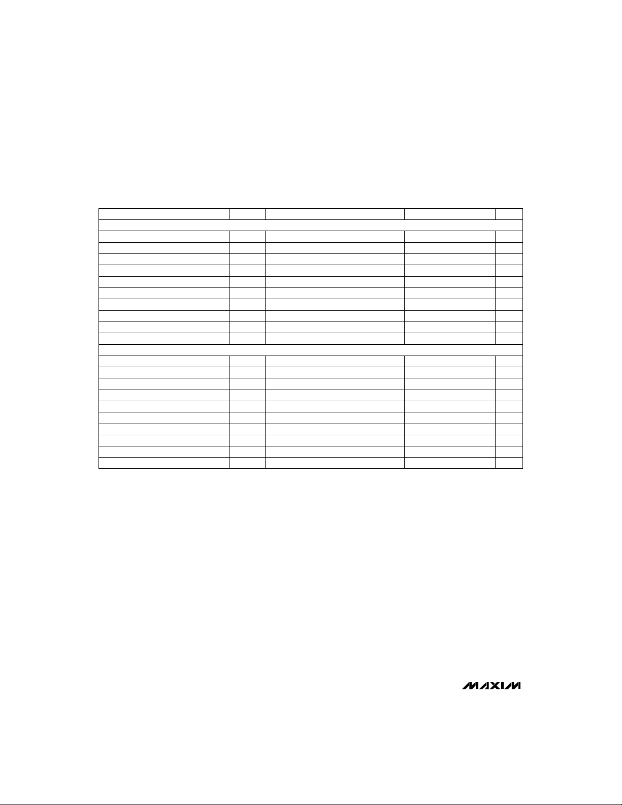
ELECTRICAL CHARACTERISTICS (continued)
(VCC= +5V, VEE= -5V, -2V ≤ VIN≤ +2V, output load resistor (RL) = 150Ω, TA= T
Typical values are at T
Logic Input High Current
Logic Input Low Current
Logic Output High Voltage
Logic Output Low Voltage
DYNAMIC SPECIFICATIONS
Input Noise Density
Settling Time
Amplifier Disable Time
Amplifier Enable Time
Channel Switching Time
Channel Switching Propagation Delay
Note 2: Defined as the DC offset shift when switching between input channels for a given output.
Note 3: Voltage Gain Accuracy for MAX458 calculated as (V
Note 4: Voltage Gain Accuracy for MAX459 calculated as (VOUT/2 - VIN) @ (VIN = +1V) - (VOUT/2 - VIN) @ (VIN = -1V)
Note 5: All logic levels are guaranteed over the range of VS= ±4.75V to ±5.25V.
Note 6: Differential phase and gain measured with a 40 IRE (285.7mV), 3.58MHz sine wave superimposed on a linear ramp of 0 IRE
Note 7: For MAX458, step input from +2V to 0V; for MAX459, step input from +1V to 0V. All unused channels grounded and all
Note 8: Test input channel programmed to an output and grounded through a 75Ω resistor. Adjacent input is programmed to an
Note 9: Same as Note 6 above, except driven input and output are not adjacent to test input/output.
Note 10: All inputs but the test input are driven by a 10MHz 4Vp-p sine wave. All outputs except the test output are connected to driven inputs.
Note 11: Same as Note 9 above, except with test channel programmed off.
to 100 IRE (714.3mV). “The IRE scale is a linear scale for measuring, in arbitrary IRE units, the relative amplitudes of the various components of a television signal” (from the “Television Engineering Handbook”, edited by K. Blair Benson, McGraw
Hill). This system defines 100 IRE as reference white, 0 IRE as the blanking level, and -40 IRE as the sync peak. The equipment used for the test signal generated 714.3mV (100 IRE) as reference white and -285.7mV (-40 IRE) as sync. The modulation used was 285.7mV (40 IRE), which conforms to the EIA color signal standards.
unused amplifiers disabled.
adjacent output and driven by a 10MHz, 4Vp-p sine wave.
= +25°C.)
A
IH
IL
OH
OL
DGDifferential Gain Error (Note 6)
DGDifferential Phase Error (Note 6)
SRSlew Rate
BWBandwidth (-3dB)
S
AOFF
AON
CSW
CPD
(Note 3)
(Note 3)
I
= 400µA (Note 5)
SOURCE
I
= 1.6mA (Note 5)
SINK
MAX458
MAX459
MAX458
MAX459
MAX458
MAX459
MAX458, RL= 75Ω
f = 10kHz
n
To 0.1% of final value (Note 7)
See
Typical Operating Characteristics
(Note 8)
(Note 9)
(Note 10)
(Note 11)
OUT - VIN) @ (VIN = +2V) - (VOUT - VIN) @ (VIN = -2V)
——————————––————————————4—V————————————————————
———————————————————————2—V——————————————————————
CONDITIONS
to T
MIN
MAX
Positive transition
Negative transition
Positive transition
Negative transition
, unless otherwise noted.
0.01
0.13
0.05
0.14
200
150
300
250
100
90MAX459, RL= 150Ω
100Switching Transient Glitch
UNITSMIN TYP MAXSYMBOLPARAMETER
µA10I
µA10I
V4.0V
V0.5V
%
degrees
V/µs
MHz
nV/√Hz20e
ns40t
ns100t
ns120t
ns60t
ns50t
mV
p-p
dB-65Adjacent Channel Crosstalk
dB-65Non-Adjacent Channel Crosstalk
dB-55All-Hostile Crosstalk
dB-60All-Hostile Off Isolation
MAX458/MAX459
_______________________________________________________________________________________ 3
Page 4
8x4 Video Crosspoint Switches with Buffers
TIMING CHARACTERISTICS (Note 12)
(VCC= +5V, VEE= -5V, -2V ≤ VIN≤ +2V, output load resistor (RL) = 150Ω, TA= T
CONDITIONS
PARALLEL-MODE TIMING (see Figure 1)
Address to –W—R–Fall Setup Time
Address to –W—R–Rise Hold Time
–C—E–
Fall to –W—R–Fall Setup Time
–C—E–
Rise to –W—R–Rise Hold Time
–W—R–
Pulse Width Low
Data to –W—R–Rise Setup Time
Data to –W—R–Rise Hold Time
–W—R–
Rise to –U—P—D—A—T—E–Fall Setup Time
–U—P—D—A—T—E–
MAX458/MAX459
Pulse Width Low
–U—P—D—A—T—E–
Rise to –W—R–Fall Setup Time
ADS
ADH
CES
CEH
WR
DS
DH
WRS
UP
UPS
SERIAL-MODE TIMING (see Figure 6)
SCLK to –C—S–Fall
–C—S–
Fall to SCLK Rise
SCLK Pulse Width High
SCLK Pulse Width Low
DIN to SCLK Rise Setup Time
DIN to SCLK Rise Hold Time
SCLK Fall to DOUT
SCLK Rise to –C—S–Rise
–C—S–
Rise to SCLK Rise
–C—S–
Pulse Width High
CSO
CSS
CH
CL
DS
DH
DO
CSH
CS1
CSW
Note 12: Timing Characteristics are guaranteed by design.
MIN
to T
, unless otherwise noted.)
MAX
UNITSMIN MAXSYMBOLPARAMETER
ns20t
ns0t
ns0t
ns0t
ns40t
ns50t
ns0t
ns0t
ns40t
ns25t
ns0t
ns35t
ns50t
ns30t
ns50t
ns0t
ns200t
ns30t
ns20t
ns100t
4 _______________________________________________________________________________________
Page 5
8x4 Video Crosspoint Switches with Buffers
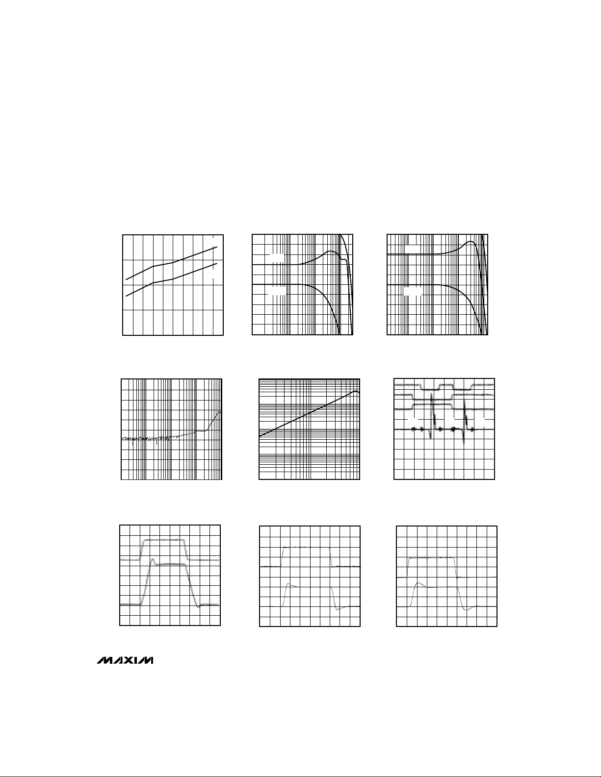
__________________________________________Typical Operating Characteristics
(TA = +25°C, unless otherwise noted.)
POWER SUPPLY CURRENT
vs. TEMPERATURE
100
80
60
CURRENT (mA)
40
20
-60 -40 -20 0 20 40 60 80 100 120 140
TEMPERATURE (°C)
CROSSTALK vs. FREQUENCY
40
0
-40
-80
AMPLITUDE (dB)
-120
I
CC
I
EE
6
4
2
MAX458/459 Fg TOC1
0
-2
-4
-6
AMPLITUDE (dB)
0.1 1 10 100 250
OUTPUT IMPEDANCE vs. FREQUENCY
MAX458/459 Fg TOC7
10
1
0.1
OUTPUT IMPEDANCE (Ω)
MAX458
GAIN vs. FREQUENCY
GAIN
PHASE
FREQUENCY (MHz)
6
MAX458/459 Fg TOC4
PHASE (DEGREES)
4
2
0
36
AMPLITUDE (dB)
72
108
144
180
UPDATE
MAX458/459 Fg TOC6
D0 & D2
GND
MAX459
GAIN vs. FREQUENCY
GAIN
PHASE
0.1 1 10 100 250
FREQUENCY (MHz)
CHANNEL SWITCH TRANSIENT
D1
OUT
MAX458/459 Fg TOC5
00
36
72
108
144
180
IN2IN5IN2
MAX458/MAX459
PHASE (DEGREES)
10V/div
(digital)
20mV/div
(analog)
0.01
0.1 10
FREQUENCY (MHz)
LARGE-SIGNAL PULSE RESPONSE
5V
2V/div
GND
1V/div
-15V
1 100
MAX458
25ns/div
+200mV
INPUT
-200mV
+100mV
OUTPUT
-100mV
MAX458/459 Fg TOC2
1 10 100
FREQUENCY (MHz)
MAX458
SMALL-SIGNAL PULSE RESPONSE
10ns/div
MAX458/459 Fg TOC8
+200mV
INPUT
-200mV
+200mV
OUTPUT
-200mV
100ns/div
MAX459
SMALL-SIGNAL PULSE RESPONSE
10ns/div
_______________________________________________________________________________________
MAX458/459 Fg TOC3
MAX458/459 Fg TOC9
INPUT
OUTPUT
5
Page 6

8x4 Video Crosspoint Switches with Buffers
______________________________________________________________Pin Description
PIN
DIP PLCC
1 DIN Serial Data Input
2, 4, 6, 8,
14, 16, 18,
27, 33, 35
3 IN0 Analog Input Channel 0
5 IN1 Analog Input Channel 1
7 IN2 Analog Input Channel 2
9 IN3 Analog Input Channel 3
10, 31 V
MAX458/MAX459
11 IN4 Analog Input Channel 4
12, 29 V
13 IN5 Analog Input Channel 5
15 IN6 Analog Input Channel 6
17 IN7 Analog Input Channel 7
19 SHDN Shutdown, active high. Connect to GND if not used.
20 DOUT Serial Data Output used for daisy-chaining devices.
21 D3 Parallel Digital Channel Input Address Bit 3
22 D2 Parallel Digital Channel Input Address Bit 2
23 D1 Parallel Digital Channel Input Address Bit 1
24 D0 Parallel Digital Channel Input Address Bit 0
25 A1 Parallel Digital Amplifier Output Address Bit 1
26 A0 Parallel Digital Amplifier Output Address Bit 0
28 OUT3 Amplifier 3 Analog Output
30 OUT2 Amplifier 2 Analog Output
32 OUT1 Amplifier 1 Analog Output
34 OUT0 Amplifier 0 Analog Output
36
37
38
39 SCLK Serial Clock43
40
— N.C. Not Internally Connected2, 6, 24, 32
Note: All GND pins must be grounded for optimum crosstalk performance.
1
3, 5, 8, 10,
16, 18, 20,
30, 37, 39
4
7
9
11
12, 35
13
14, 33
15
17
19
21
22
23
25
26
27
28
29
31
34
36
38
40
41
42
44
NAME
GND Ground
Positive Power Supply (+5V). Connect both VCCpins to the positive supply.
CC
Negative Power Supply (-5V). Connect both VEEpins to the negative supply.
EE
–C—E–
–W—R–
–U—P—D—A—T—E–
–C—S–
Chip Enable, used in parallel mode. Keep high for serial operation.
Write Low, latches input registers in parallel mode. Hold high for serial operation.
Update Low, latches amplifier registers in parallel mode. Hold high for serial operation.
Chip Select, used in serial operation. Hold high for parallel mode of operation.
FUNCTION
6 _______________________________________________________________________________________
Page 7

8x4 Video Crosspoint Switches with Buffers
2
IN0
IN1
IN2
IN3
V
CC
IN4
75Ω
75Ω
75Ω
75Ω
0.1µF
75Ω
3
4
5
6
7
8
9
10
11
MAX458
MAX459
OUT0
ENABLE
35
OUT0
75Ω
75Ω
34
33
MAX458/MAX459
0.1µF
V
EE
IN5
IN6
IN7
PIN NUMBERS APPLY TO DIP PACKAGE.
75Ω
75Ω
75Ω
12
13
14
15
16
17
18
IN0
IN7
IN0
IN7
IN0
IN7
24
D0 D1 D2 D3
Figure 1. Block Diagram and Typical Operating Circuit
OUT1
ENABLE
OUT2
ENABLE
OUT
ENABLE
23 22 21 26 25
OUT3
4
ENABLE
A0 A1
PARALLEL INTERFACE
1
20
39
40
19
OUT1
32
31
OUT2
30
29
OUT3
28
27
38
37
36
CE
0.1µF
0.1µF
WR
75Ω
75Ω
75Ω
UPDATE
DIN
DOUT
SCLK
CS
SHDN
V
CC
V
EE
SERIAL INTERFACE
75Ω
75Ω
75Ω
_______________________________________________________________________________________ 7
Page 8

8x4 Video Crosspoint Switches with Buffers
ANALOG INPUTS
IN7IN0
UPDATE
WR
CE
INPUT
REGISTER
1
CONTROL
SWITCH
REGISTER
1
7
• • •
0
• • •• • •• • •• • •
8-1 MUX
MAX458/MAX459
• • •
OUT0
MAX458
MAX459
INPUT
REGISTER
2
CONTROL
A0
A1
INPUT
REGISTER
3
CONTROL
INPUT
REGISTER
4
CONTROL
D0
D1
D2
D3
L = TRANSPARENT
H = LATCHED
CS = HIGH, SCLK = DIN = LOW
SWITCH
REGISTER
2
SWITCH
REGISTER
3
SWITCH
REGISTER
4
0
8-1 MUX
7
• • •
0
8-1 MUX
7
• • •
0
8-1 MUX
7
OUT1
OUT2
OUT3
Figure 2. Parallel-Logic Block Diagram
8 _______________________________________________________________________________________
Page 9

8x4 Video Crosspoint Switches with Buffers
_______________Detailed Description
The MAX458/MAX459 video crosspoint switches consist
of a high-speed 32 (8x4) switch array with wide-bandwidth line drivers (Figure 1). This design allows makebefore-break switching to reduce output noise and
glitches, but the inputs will not short together. It also provides high input impedance and low input capacitance,
so no input buffer amplifier is needed. However,
because different transistors provide gain depending on
the input selection, the DC offset voltage shifts slightly
when a new input is switched in. The change in offset
voltage is typically 3mV.
All output buffers will drive back-terminated 50Ω, 75Ω,
or higher impedance lines with up to 100pF capacitance. The amplifier outputs can be disabled, which is
useful for creating large arrays. When disabled, the
MAX458 presents an output impedance of approximately 1MΩ. The MAX459 disabled output impedance
is 1kΩ (to ground), due to the internal feedback resistors used to achieve the gain of two.
During power-on, if –C—S–and –U—P—D—A—T—E–are held high, all
output amplifiers are disabled. In a large array, this
feature prevents two ON paralleled amplifiers from distorting each other’s signals. The amplifiers can be programmed to come up in any state simultaneously at any
time after power-on. See the
section.
1
DIN
MAX458
MAX459
19
SHUTDOWN
Pin numbers apply to DIP package.
Figure 3. Parallel Connection (only logic pins shown)
SHDN
20
DOUT
Analog Section
Creating Large Arrays
40
CS
V
CC
39
SCLK
38
37
WR
36
CE
26
A0
25
A1
24
D0
23
D1
22
D2
21
D3
UPDATE
WRITE
CHIP ENABLE (SELECT)
AMPLIFIER SELECT A0
AMPLIFIER SELECT A1
DATA BIT D0
DATA BIT D1
DATA BIT D2
DATA BIT D3
UPDATE
The MAX458/MAX459 have two register banks—an
Digital Section—Parallel Mode
input register and a switch register (Figure 2). Each of
these registers is either latched (when the control input
is high) or transparent (when the control input is low).
The input register is controlled by –W—R–and –C—E–and is
selected by the decode of A0 and A1. If both –W—R–and
–C—E–
are low, the input register selected by A0 and A1 is
transparent, and the state of D0–D3 is presented to the
switch register. The other three input registers remain
latched. If D0–D3 change before –U—P—D—A—T—E–is asserted
(goes low), the new data (the changed D0–D3) will then
be latched in the switch register. If –W—R–or –C—E–is high, all
input registers are latched and their data is presented
Table 1. Amplifier Selection
Output Amplifier SelectedA0A1
L L
L
H
H
H
L
H 3
0
1
2
Table 2. Input Selection
D0D1
Input Channel SelectedD2D3
L L
L
L
L
L H
L
L
Table 3. Writing Data
–W—R––C—E–
HXX
H
H
X
X
H
L
L
L
L
L L
L
L
L
L 3
H
H
H 7
–U—P—D—A—T—E–
H
H
L
L
H
L
H
H
L
H
H
L L
L
H
H
L
H
HL
X XH X
Disable output amplifier
selected by A0, A1.
FUNCTION
Device not selected or is operating in serial mode. Both registers are latched.
Data in input registers passes through
switch registers. Output reflects data in
input registers.
Input register of selected amplifier is transparent. Switch registers are latched. Other
input registers are latched.
All switch registers and selected input register are transparent. Selected amplifier (chosen by state of A0, A1) reflects input data.
Other amplifiers reflect data that had been
latched into the input registers previously.
0
1
2
4
5
6
MAX458/MAX459
_______________________________________________________________________________________ 9
Page 10

8x4 Video Crosspoint Switches with Buffers
to their switch registers. As long as either –W—R–or –C—E–is
high, the input register will not change. The switch register will pass any new data on the falling transition of
–U—P—D—A—T—E–
.
Each register of the switch-register bank controls the
inputs to one amplifier. With –U—P—D—A—T—E–low, the switch
registers are transparent and switch connection is controlled by the input register. However, if –U—P—D—A—T—E– is
high, the switch register is latched and any change in
data by the input register will not affect the amplifier
output state. Two register banks are used so that data
can be loaded into input registers without affecting the
switch/amplifier selection. This allows amplifiers to be
programmed and then changed simultaneously. When
the registers are not latched, they are made transparent.
Use data bit D3 to disable the amplifier selected by
MAX458/MAX459
A0–A1 and place its output in high-impedance mode.
As an example, the code to disable OUT0 is as follows:
Pin Name: D3 D2 D1 D0 A1 A0
Input Code: 1 X X X 0 0
When operating in parallel mode, C—S–must be wired high
and SCLK and DIN should be grounded, as shown in
Figure 3. Refer to Figure 4 for the correct timing relationships.
The MAX458/MAX459 use a three-wire serial interface
Digital Section—Serial Mode
that is compatible with SPI, QPSI and Microwire interfaces. Serial mode, shown in Figure 5, is enabled
when –W—R–, –U—P—D—A—T—E–, and –C—E–are held high and –C—S–goes
low. Figures 6 and 7 show serial-mode timing. Figure 8
shows the MAX458/MAX459 configured for serial operation. Figure 9 shows the Microwire connection, and
Figure 10 shows the SPI/QSPI connection.
The serial output, DOUT, allows cascading of two or
more crosspoint switches to create larger arrays. The
data at DOUT is delayed by 16 cycles plus one clock
pulse width at DIN. DOUT changes on SCLK’s falling
edge when –C—S–is low. When –C—S–is high, DOUT remains
in the state of the last data bit.
The MAX458/MAX459 input data in 16-bit blocks. SPI
and Microwire interfaces output data in 8-bit blocks,
thereby requiring two write cycles to input data. The
QSPI interface allows variable word lengths from 8 to 16
bits and can be loaded into the crosspoint in one write
cycle. SPI and Microwire limit clock rates to 2MHz, while
the QSPI maximum clock rate is 4MHz.
A0/A1
t
ADS
CE
WR
D0–D3
UPDATE
Figure 4. Parallel-Mode Timing
10 ______________________________________________________________________________________
t
CES
ADDRESS VALID
t
WR
t
DS
DATA VALID
t
ADH
t
CEH
t
DH
t
WRS
t
UP
t
UPS
Page 11

8x4 Video Crosspoint Switches with Buffers
MAX458/MAX459
DIN
SCLK
IN7IN0
• • •• • •• • •• • •
• • •
ANALOG INPUTS
8-1 MUX
CONTROL INPUT
• • •
8-1 MUX
• • •
8-1 MUX
• • •
OUT0
OUT1
OUT2
CS
ONE
SHOT
D
MAX458
MAX459
IN
CLK
Q
16-BIT
SHIFT
REGISTER
SWITCH
REGISTER
0
SWITCH
REGISTER
1
SWITCH
REGISTER
2
0
7
0
7
0
7
Q
D
DOUT
Figure 5. Serial-Mode Logic Block Diagram
______________________________________________________________________________________ 11
OUT
WR = CE = UPDATE = HIGH
SWITCH
REGISTER
3
L = TRANSPARENT
H = LATCHED
0
8-1 MUX
7
OUT3
Page 12

8x4 Video Crosspoint Switches with Buffers
CS
t
CS0
SCLK
DIN
DOUT
DATA FROM PREVIOUS WRITE CYCLE
t
CSS
t
DS
t
CH
t
DH
D0
D3 (OUT3) D2 (OUT3) D1 (OUT0) D0 (OUT0)
D3
Figure 6. Serial-Mode Timing
MAX458/MAX459
CS
SCLK
DIN
D3 D2 D1 D0 D3 D2 D1 D0 D3 D2 D1 D0 D3 D2 D1 D0
OUT3 OUT2 OUT1 OUT0
DOUT
D3 D2 D1 D0 D3 D2 D1 D0 D3 D2 D1 D0 D3 D2 D1 D0
DATA FROM PREVIOUS WRITE CYCLE
Figure 7. Serial-Mode Data Sequence
1
SERIAL
DATA IN
DIN
MAX458
MAX459
19
SHDN
20
SERIAL
DATA OUT
Pin numbers apply to DIP package.
DOUT
Figure 8. Serial Connection (only logic pins shown)
CS
SCLK
UPDATE
WR
CE
A0
A1
D0
D1
D2
D3
40
CHIP SELECT
39
38
37
36
26
25
24
23
22
21
t
CS1
SK
MICROWIRE
SO
PORT
I/O
SI
t
CSW
D3
t
CSH
• • •
t
CL
• • •
• • •
t
D0
• • •
D2 D1 D0 D3
SERIAL
CLOCK
V
CC
V
CC
V
CC
THE DOUT-SI CONNECTION IS NOT REQUIRED FOR
WRITING TO THE MAX458/MAX459, BUT MAY BE USED
FOR DATA-ECHO PURPOSES.
MAX458
MAX459
SCLK
DIN
CS
DOUT
Figure 9. Microwire Connection
12 ______________________________________________________________________________________
Page 13

8x4 Video Crosspoint Switches with Buffers
IN_
SCLK
DIN
MAX458
MAX459
THE DOUT-MOSO CONNECTION IS NOT REQUIRED FOR
WRITING TO THE MAX458/MAX459, BUT MAY BE USED
FOR DATA-ECHO PURPOSES.
CS
DOUT
SCK
SPI/QSPI
MOSI
PORT
I/O
MOSO
CPOL = 0, CPHA = 0
RETURN
CURRENT
RETURN
CURRENT
IN_
GROUND PLANE
MAX458/MAX459
Figure 10. SPI/QSPI Connection
__________Applications Information
Grounding and Bypassing,
PC Board Layout
As with all analog circuits, good PC board layout, proper grounding, and careful component selection are crucial for realizing the full AC performance of high-speed
amplifiers such as the MAX458/MAX459. For optimal
performance:
1) Use a large, low-impedance analog ground plane.
With multilayer boards, the ground plane(s) should
be located on the layer that does not contain signal
traces. Connect all GND pins to the analog ground
plane.
2) Minimize trace area at the circuit’s critical high-impedance nodes to prevent unwanted signal coupling.
Surround analog inputs with an AC ground trace
(bypassed DC power supply, etc.). The analog input
pins of the MAX458/MAX459 have been separated
with AC ground pins (GND, VCC, VEE) to minimize
parasitic coupling, which can degrade crosstalk.
3) Connect the coaxial-cable shield to the ground side
of the 75Ω terminating resistor at the ground plane
to further reduce crosstalk (Figure 11).
4) Bypass all power-supply pins directly to the ground
plane with 0.1µF ceramic capacitors placed as
close to the supply pins as possible. For high-current loads, you may need 10µF tantalum or aluminum-electrolytic capacitors in parallel with the
0.1µF ceramics. Keep capacitor lead lengths as
short as possible to minimize series inductance; surface-mount chip capacitors are ideal.
Figure 11. Low-Crosstalk Layout. Return current from termination resistor does not flow through the ground plane.
Creating Larger Arrays
The MAX458/MAX459 assume a high-impedance state
on power-up if the inputs are not being programmed to
any particular state during that time. They also are in a
high-impedance state when disabled. This feature
makes it possible to create larger arrays than 8x4 without special programming, other than ensuring that your
program doesn’t turn on two paralleled outputs simultaneously. Testing has shown no degradation of differential gain or phase when the outputs are connected in
parallel.
The MAX458/MAX459’s input registers remain active during shutdown, which allows the crosspoint to be programmed while the devices are shut down. As a result, all
outputs may be simultaneously brought to any state,
including disabled. Just program all of the MAX458/
MAX459s into shutdown, and enter the program of your
choice by selecting the desired inputs and outputs. Taking
SHDN low takes the device(s) out of shutdown.
A power-on reset circuit causes the output amplifiers to
power up in the disabled mode, whether or not SHDN
is applied, if –U—P—D—A—T—E–and –C—S–are high.
The number of MAX458s that can be paralleled is limited by capacitive loading on each output, which must
not exceed 100pF. Each input presents approximately
7pF of load, and each output presents approximately
12pF. Therefore, the MAX458/MAX459 will drive a maximum of 14 inputs, or 7 outputs and 2 inputs, or any
other combination resulting in less than a 100pF load.
Adding isolation resistors enables more MAX458s to be
paralleled (see the
Driving Capacitive Loads
section).
______________________________________________________________________________________ 13
Page 14

8x4 Video Crosspoint Switches with Buffers
When driving loads greater than 100pF, you may need
Driving Capacitive Loads
a capacitance compensating resistor in series with the
output of each affected amplifier. The required resistor
will depend on load as well as capacitance. For 150Ω
or higher load resistances and capacitance up to
1000pF, use a 2.4Ω resistor. For 100Ω loads, use a
4.7Ω resistor.
If an output amplifier is loaded with a pure capacitance
or with the inputs of other MAX458/MAX459s, the resistors will cause no degradation of gain or other performance because of the high impedance of the
crosspoints. However, resistive loads may cause a
reduction in gain.
MAX458/MAX459
The serial output, DOUT, allows cascading of two or
Daisy-Chaining Devices
more crosspoint switches to create larger arrays. The
data at DOUT is the DIN data delayed by 16 cycles
plus one clock width. DOUT changes on SCLK’s falling
edge when –C—S–is low. When C—S–is high, DOUT remains
in the state of the last data bit.
Any number of MAX458/MAX459 crosspoint switches
can be daisy-chained by connecting the DOUT of one
device to the DIN of the next device in the chain, as
shown in Figure 12. For proper timing, ensure that both
t
(C—S–low to SCLK high) and tCLare greater than
CSS
tDO+ tDS.
DOUT is a TTL-compatible output with an active pull-
up. It does not become high impedance when C—S–is
high.
CS
SCLK
SERIAL
1
DATA
INPUT
DOUT
20
1
DIN
20
DOUT
Figure 12. 16x4 Crosspoint Switch Using Serial "Daisy Chain"
Connection
MAX458
MAX459
MAX458
MAX459
40
39
28
30
32
34
40
39
28
30
32
34
OUT3
OUT2
OUT1
OUT0
14 ______________________________________________________________________________________
Page 15

8x4 Video Crosspoint Switches with Buffers
____Pin Configurations (continued)
TOP VIEW
DIN
GND
IN0
GND
IN1
GND
IN2
GND
IN3
V
IN4
V
IN5
GND
IN6
GND
IN7
GND
SHDN
DOUT
1
2
3
4
MAX458
MAX459
5
6
7
8
9
CC
10
11
12
EE
13
14
15
16
17
18
19
20
40
39
38
37
36
35
34
33
32
31
30
29
28
27
26
25
24
23
22
21
CS
SCLK
UPDATE
WR
CE
GND
OUT0
GND
OUT1
V
CC
OUT2
V
EE
OUT3
GND
A0
A1
D0
D1
D2
D3
DIP
MAX458/MAX459
______________________________________________________________________________________ 15
Page 16

8x4 Video Crosspoint Switches with Buffers
________________________________________________________Package Information
INCHES MILLIMETERS
DIM
D1
A2
MAX458/MAX459
A
A1
L
e
D
A
A1
A2
A3
B
B1
C
D
D1
E
E1
e
e
A
e
B
L
α
A3
E
E1
α
C
e
B1
B
A2
C
DD1
A
e
B
DIM
A
A1
A2
A3
B
e
D2
B1
B
B1
C
D
D1
D2
D3
e
MAX
MIN
–
0.015
0.125
0.055
0.016
0.045
0.008
2.025
0.050
0.600
0.525
0.100 BSC
0.600 BSC
–
0.120
0˚
0.200
–
0.175
0.080
0.020
0.065
0.012
2.075
0.090
0.625
0.575
0.700
0.150
15˚
MIN
–
0.38
3.18
1.40
0.41
1.14
0.20
51.44
1.27
15.24
13.34
2.54 BSC
15.24 BSC
–
3.05
0˚
40-PIN PLASTIC
DUAL-IN-LINE
PACKAGE
INCHES MILLIMETERS
MAX
MIN
0.165
0.100
0.145
0.020
0.013
0.026
0.009
0.685
0.650
0.590
0.180
0.110
0.156
–
0.021
0.032
0.011
0.695
0.655
0.630
MIN
4.19
2.54
3.68
0.51
0.33
0.66
0.23
17.40
16.51
14.99
12.70 REF0.500 REF
1.27 REF0.050 REF
MAX
5.08
–
4.45
2.03
0.51
1.65
0.30
52.71
2.29
15.88
14.61
17.78
3.81
15˚
21-348A
MAX
4.57
2.79
3.96
–
0.53
0.81
0.28
17.65
16.64
16.00
21-350A
D3
D1
D
A3
A1
A
44-PIN PLASTIC
LEADED CHIP
CARRIER
PACKAGE
16 ______________________________________________________________________________________
 Loading...