

Page 1
19-0302; Rev 0; 9/94
Low-Cost, High-Resolution, 200MHz
Video CRT Driver
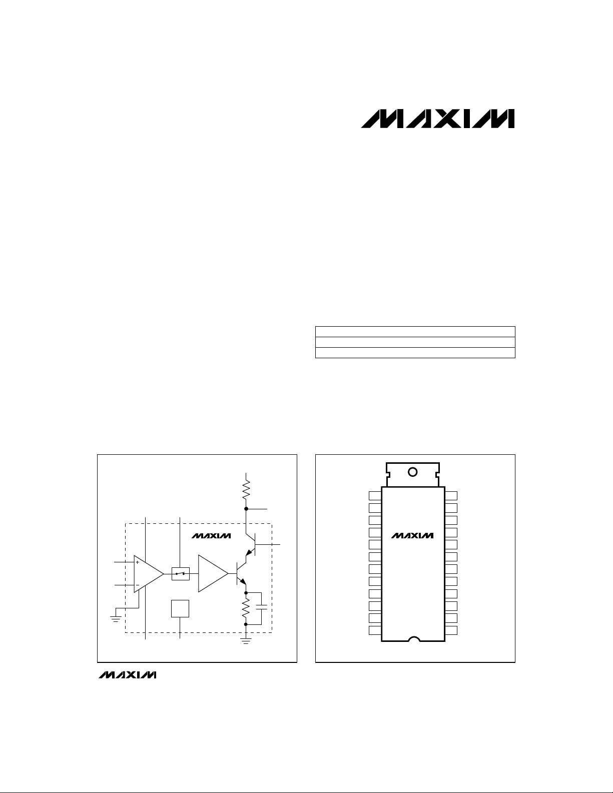
_______________General Description
The MAX445 is a high-performance, monolithic, variablegain transconductance amplifier with a high-voltage
open-collector output capable of directly driving a video
display (CRT cathode). A 2.5ns rise time is achieved
using a peaking network with a 200Ω load resistor and
an 8pF total load (CRT and parasitic capacitance).
Differential inputs and a linear adjustable gain stage
with an output offset adjustment make the versatile
MAX445 well suited for many video display applications. A buffered bandgap reference voltage is available for the gain (contrast) and offset adjustments
along with a TTL BLANK input to turn off the output current, independent of signal input.
The MAX445 is available in a 24-pin power-tab DIP
package. A suitable heatsink must be attached to
maintain the junction temperature within the recommended operating range.
________________________Applications
CRT Driver for High-Resolution Monochrome and
Color Displays
High-Voltage, Variable-Gain Transconductance
Amplifier
________________Functional Diagram
V
AA
____________________________Features
♦ 2.5ns Rise/Fall Time into an 8pF Load
♦ 200MHz Small-Signal Bandwidth
♦ 50Vp-p Output
♦ Ground Referenced Differential Inputs
♦ Linear Variable Gain for Contrast Control
♦ Offset Adjustment for Black Level
♦ 5.5V Bandgap Reference
♦ Drives 1280 x 1024 and 1530 x 1280 Displays
______________Ordering Information
PART
MAX445CPG
MAX445C/D 0°C to +70°C**
* Case temperature range, T
Maximum Ratings and Applications Information for thermal/heat
sink considerations.
**Dice are specified at TJ= +25°C, DC parameters only.
TEMP. RANGE PIN-PACKAGE
0°C to +70°C*
CASE
24 Power-Tab DIP
Dice
= 0°C to +90°C. See Absolute
__________________Pin Configuration
TOP VIEW
MAX445
R
VIN+
VIN-
GNDA
L
V
CONTRAST
BLANK
IOUT
MAX445
BAND
GAP
VREF
CURRENT
AMP
GND
PRE-AMP
OFFSET
________________________________________________________________
OUT
VCB
GND
VREF
OFFSET
CONTRAST
GNDA
VINVIN+
V
BLANK
GND
1
2
3
4
MAX445
5
6
7
V
EE
8
V
EE
9
CC
10
11
12
Power-Tab DIP
Maxim Integrated Products
Call toll free 1-800-998-8800 for free samples or literature.
GND
24
GND
23
GND
22
V
EEO
21
N.C.
20
IOUT
19
N.C.
18
VCB
17
VCB
16
GND
15
GND
14
GND
13
1
Page 2
Low-Cost, High-Resolution, 200MHz
Video CRT Driver
ABSOLUTE MAXIMUM RATINGS
VAAOutput Supply.................................................................80V
Output Supply with Respect to VCB...............................70V
V
AA
VCB Common-Base Supply...................................................20V
Positive Supply............................................................12.5V
V
CC
Negative Supply..........................................................-12.5V
V
EE
Differential Input Voltage..........................................................2V
Common-Mode Input Voltage................................................±2V
MAX445
Contrast Input Voltage.................................................-1V to +6V
Stresses beyond those listed under “Absolute Maximum Ratings” may cause permanent damage to the device. These are stress ratings only, and functional
operation of the device at these or any other conditions beyond those indicated in the operational sections of the specifications is not implied. Exposure to
absolute maximum rating conditions for extended periods may affect device reliability.
ELECTRICAL CHARACTERISTICS
(VAA= 20V, VCB = 10V ±0.5V, VCC= 10V ±0.5V, VEE= -10.5V ±0.5V, VIN = (VIN+) - (VIN-) = 0V, CONTRAST = 1.0V,
OFFSET = 1.0V, R
Output-Common-Base Supply Current
Positive Supply Current
Negative Supply Current
Low Blank Input Bias Current
High Blank Input Bias Current
Contrast Input Bias Current
Offset Input Bias Current
VIN+ or VIN- Signal Input Current
VIN+ or VIN- DC Input Impedance
VIN+ or VIN- Input Capacitance
Reference Output Voltage
Output Current (Blanked)
Output Current
Output Current Change vs. Temperature
Output Current Change vs. Contrast ADJ
Output Current Change vs. VIN, Blanked
Amplifier Linearity Error (∆Gm/∆VIN)
Contrast Linearity Error (∆Gm/∆Contrast)
= 0Ω, BLANK = 0.4V, T
L
to VIN
OUT
= +25°C, unless otherwise noted.)
CASE
CB
CC
I
VEE
VCC, VEE= ±5%, VIN = +250mV,
CONTRAST = 5.0V, referred to input
BLANK = 0.4V
IL
BLANK = 2.4V
CONTRAST = 5.0V
OFFSET = 1.0V
VCM= ±0.5V, CONTRAST = 5.0V
IN
I
LOAD
BLANK = 2.4V, OFFSET = 1V, VAA= 75V
BLANK = 2.4V, OFFSET = 3V
OFFSET = 0V, CONTRAST = 4.0V
OFFSET = 5.0V, CONTRAST = 1V
TC= +25°C to +90°C
CONTRAST = 0V to 5V
BLANK = 2.4V, CONTRAST = 5.0V,
∆VIN- = 0.3V
CONTRAST = 5.0V
CONTRAST = 1.0V
CONTRAST = 0V
CONTRAST = 4.0V, OFFSET = 1.0V
VIN = 0.2V, OFFSET = 0V
OFFSET = 0V, R
∆I
∆I
∆I
I
OUT
I
OUT
GmTransconductance, I
EE
IH
IC
IB
IS
VIN
REF
OUT
OUT
OUT
Offset Input Voltage.....................................................-1V to +6V
Blank Input Voltage.....................................................-1V to +6V
Bandgap-Reference Output Current...................................-5mA
Continuous Power Dissipation
derate at 170mW/°C above T
Operating Junction Temperature ......................-55°C to +150°C
Storage Temperature.........................................-55°C to +150°C
Lead Temperature (soldering, 10sec).............................+300°C
CONDITIONS
+ I
VEEO
= 2mA
= 100Ω
LOAD
= +90°C.......................10W
CASE
-0.1 25
80 140
400 600
70 120
-25 25
±1
±1
UNITSMIN TYP MAXSYMBOLPARAMETER
mA40I
mA70I
mA-100I
dB25PSRRPower-Supply Rejection Ratio
mA-0.6 0I
mA-0.4 0I
µA010I
µA010I
µA-50 50I
dB36CMRRInput Common-Mode Rejection Ratio
kΩ10R
pF2C
V5.25 5.75V
mA
mA
mA±3
mA±10
mA±1
mA/V
%±2
%±3
MHz200BWBandwidth, 3dB
2 _______________________________________________________________________________________
Page 3
Low-Cost, High-Resolution, 200MHz
Video CRT Driver
ELECTRICAL CHARACTERISTICS (continued)
(VAA= 20V, VCB = 10V ±0.5V, VCC= 10V ±0.5V, VEE= -10.5V ±0.5V, VIN = (VIN+) - (VIN-) = 0V, CONTRAST = 1.0V,
OFFSET = 1.0V, R
Rise/Fall Time (10% to 90%)
Settling Time (90% to 100% ±2%)
= 0Ω, BLANK = 0.4V, T
L
= +25°C, unless otherwise noted.)
CASE
CONDITIONS
RL= 200Ω,
tr, t
CL= 8pF,
f
VAA= 75V,
tr(VIN) < 1ns,
CL= 8pF, no peaking
s
No peaking,
OUTp-p = 50V
With peaking,
OUTp-p = 45V
UNITSMIN TYP MAXSYMBOLPARAMETER
3.6
ns
2.5
ns8t
%±2Thermal Distortion
______________________________________________________________Pin Description
PIN
1, 12, 13, 14,
15, 22, 23, 24
2 VREF Reference Output (+5.5V)
3 OFFSET Output Voltage Offset-Adjustment Input
4 CONTRAST Output Gain-Adjustment Input
5 GNDA Pre-Amp Ground
6 VIN- Inverting Signal Input
7 VIN+ Noninverting Signal Input
8, 9 V
10 V
11 BLANK Blanking Input, TTL
16, 17 VCB Output Common-Base Supply (+10V)
18, 20 N.C. No Connection—leave open
19 IOUT Open-Collector Current Output
21 V
NAME FUNCTION
GND High-Current Ground. Connect all pins to ground plane.
EE
CC
EEO
Negative Supply (-10.5V)
Positive Supply (+10V)
Negative Supply for Output Stage (-10.5V)
MAX445
_______________________________________________________________________________________ 3
Page 4

Low-Cost, High-Resolution, 200MHz
Video CRT Driver
__________Applications Information
VIN+ and VIN- are differential video input pins designed
to allow DC coupling of a 0V to +1V signal into VIN+, with
respect to VIN-. For correct operation, it is recommended that the signals applied to these inputs be kept within
±1V, with respect to ground. Although large signals and
MAX445
offsets can be handled safely without damage, exceeding these limits may cause output linearity to suffer.
The contrast control is the overall DC-gain control that
will vary the voltage gain from 0V/V to -90V/V (with a
200Ω load resistor). An internal reference supply pin,
VREF, provides the nominal 5.5V needed to drive the
contrast input. Normally, a 5kΩ potentiometer between
VREF and ground is used to vary the contrast, but an
external source can be used instead of VREF, with some
degradation of gain stability with temperature.
The contrast control is a linear relationship. Vary the
input from 0V to 5V to achieve a voltage-gain range of
0V/V to -90V/V. This yields the following relationship for
overall voltage gain of this device (for IOUT < 250mA):
V
(-10.5V)
ANALOG
INPUT
BLANK
* STACK POLE 57-0180 OR
INDIANA GENERAL F-1650-H
Figure 1. Typical Connection Diagram
D1
EE
1N4152
50V
0.1µF
0.1µF
5k
0.1µF
5k
25Ω
50Ω
Differential Inputs
Contrast Control
+10V
D2
1N4152
BEAD*
50V
10 1716
V
CC
2
VREF
3
OFFSET
4
CONTRAST
6
VIN-
7
VIN+
11
BLANK
GNDA GND
5 24*
MAX445
0.1µF
24Ω
VCB
V
V
EE
EE
89
-10.5V
D3
1N486A
100V
BEAD*
VCB
21
VEEO
VAA- VO= [VIN(Gm) + V
VAA- VO= [VIN(V
CONTRAST
OFFSET
) (0.09) + V
The MAX445’s overall gain can vary by ±20% due to
normal process variations of internal components. Also,
if multiple devices are used in a system, all devices
must track thermally (i.e., a common heatsink).
The offset control is used to set the output quiescent
current from 5mA to 110mA (typ) when the control input
is adjusted from 0V to 5V. Normally, offset is adjusted
using a 5kΩ potentiometer between VREF and ground.
When asserted (BLANK = TTL high), this input will disable the video signal and allow the output to rise to the
VAAsupply independent of offset control.
Bandgap Reference
VREF is a bandgap bias reference for easy adjustment
of the offset and contrast inputs. This reference has a
nominal output voltage of 5.5V ±5% that can source up
to 4mA.
V
AA
(+75V)
R
L
200Ω
10W
CB
L2
L1
L1, L2, L3, AND CB ARE
ELEMENTS OF THE PEAKING COIL.
IS THE TOTAL INDUCTANCE
L
S
TO THE CATHODE. R
ARC PROTECTION ELEMENT.
C
R
100Ω
1
W (CARBON)
2
L
S
SECTION.
IOUT
10pF
22µF
100V
D4
19
L3
NOTES:
COMBINES CRT CATHODE, AND PARASITIC C.
C
L
D4 (PHILIPS BAV20 OR HITACHI 1SS91) IS ARC PROTECTION DIODE.
APPLICATIONS INFORMATION
SEE
0.1µF
(0.02)] (RL)
(0.02)] (RL)
OFFSET
Offset Control
Blank Control
IS A SERIES
S
R
S
C
L
4 _______________________________________________________________________________________
Page 5

Low-Cost, High-Resolution, 200MHz
Video CRT Driver
The MAX445’s output is an open collector of a cascode
amplifier. This output is designed to work with nominal
output supplies of VAA= +75V. The high-voltage supply
must be greater than any applied VCB voltage for proper
operation. The MAX445 sinks up to 250mA. Optimum
performance into a capacitive load can be achieved
when an impedance-matching network is used.
VCB
IOUT
The output stage consists of a common-base, high-voltage
stage and a high-speed, low-voltage current amplifier in a
cascode arrangement. The VCB input is the base connection to the common-base device of this stage. Be sure to
provide a stable DC voltage at this pin of nominally +10V.
High-frequency compensation at this input is required to
avoid output oscillations. Use a series 24Ω resistor to sup-
ply, shunted with a 10pF capacitor to ground (Figure 1).
Smaller values of this RC combination will improve output
rise/fall times, but can cause output oscillations.
Power Supplies
+10V and -10.5V supplies are required for proper operation. These supplies can be set to ±12V for convenience, however this will add additional component
power dissipation. The high-voltage supply, VAA, can be
any voltage between VCB + 10V and VCB + 65V.
V
(pin 21) is the negative supply to the output stage
EEO
and must be DC connected to VEE(pins 8 and 9), the
most negative voltage applied to the device. However,
V
must be decoupled from VEEto prevent output
EEO
oscillations. A ferrite bead and separate 0.1µF decoupling capacitors, as shown in Figure 1, will provide
appropriate decoupling.
Power-Supply Sequencing
Power-supply sequencing is important to avoid internal
device latchup. To avoid sequencing problems, external
diodes should be placed from VEEto ground, from
ground to VCC, and from VCCto the output supply (VAA),
as shown in Figure 1. With diodes used as shown, special power-supply sequencing is not required.
CRT Arc Protection
The MAX445 must be protected from electrostatic discharge (“arcs”) from the CRT. It is recommended that the
output be clamped with a low-capacitance (less than
2pF) diode to the VAAsupply. The peak current-handling
capability required of the diode is a function of the CRT
arc characteristics, but typically should be 1A or more,
such as Philips BAV20 or Hitachi 1SS91. For additional
information regarding arc protection, contact Maxim’s
applications department.
For maximum speed from the MAX445, be sure to
Impedance Matching Network
“match” the output to the CRT. Figure 1’s typical connection diagram shows a network (including parasitic reactances) associated with arc protection devices, CRT
wiring and grid structure, and load resistors. These parasitic reactances are all detrimental to good transient
response and should be minimized as much as possible.
CLis the grid-to-cathode capacitance of the CRT, plus
any parasitic capacitance to ground associated with the
cathode structure. This capacitance varies from tubetype to tube-type over the 4pF to 12pF range.
In Figure 1, LSis the inductance of the lead from the
amplifier board to the CRT cathode and the return path
from the grid to circuit ground. A wire in free space has
an inductance of 20nH/inch to 25nH/inch. With care, the
total path through the CRT gun can be kept at 1.5 to 2
inches, such that LSranges from 30nH to 50nH.
Excessive lead length will cause undesirable overshoot
and ringing in the transient response.
The peaking networks assume that 2pF of parasitic
capacitance is associated with the CRT arc protection
diode connected at the junction of L3 and L1.
Lr is the parasitic inductance of the load resistor, RL. In
some cases, CRmay be needed to improve step
response.
RSis a damping resistor in series with the CRT grid.
It also provides current limiting in the event of CRT
arcing.
The equations for determining optimum peaking network values are as follows:
L1 = (RL)2(CL) / 4
L2 = 3(RL)2(CL) / 4
CB= CL/ 5
RS= RL/ 2
L3 = k3(RL)2[2.5 x 10
CR(optional) = Lr / (2R
k3is an empirically determined factor increasing with
CLand varying from 0 for CL~ 2pF to 1 for CL~ 12pF.
However, L3 >100nH will compromise large-signal performance.
Table 1 shows peaking networks for the nominal load,
RL= 200Ω (and RS= 100Ω).
Optimum peaking depends on board layout and CRT
construction. The values given by these equations
should be used as starting points for empirically determining optimum values.
-12
L
]
2
)
MAX445
_______________________________________________________________________________________ 5
Page 6

Low-Cost, High-Resolution, 200MHz
Video CRT Driver
Table 1. Peaking Networks
(RL= 200Ω, RS= 100Ω)
CL(pF) L3 (nH) L1 (nH) L2 (nH) CB(pF) tR(ns)
2 0 20 60 0.4 1.7
4 0 40 120 0.8 1.9
6 20 60 180 1.1 2.1
MAX445
8 50 80 240 1.5 2.3
10 75 100 300 2.0 2.7
12 100 120 360 2.2 3.0
Inductors L1, L2, and L3 should be air or ferrite-core
coils with self-resonant frequencies higher than
500MHz.
The MAX445 can dissipate a large amount of power
depending on speed and load-driving requirements. The
power-tab package provides a low thermal resistance
path from the chip to an external heatsink. Be sure the
board design provides sufficient heatsinking capacity for
the intended operating range. When mounting to a chassis, it should be noted that the device tab is attached to
VEE(-10.5V). This tab should be electrically isolated from
ground through a thermally conductive insulator.
It is highly recommended that the external heatsink be
connected to ground, since an arc or electrostatic discharge entering the heatsink may break down or
bypass the tab insulator and damage the device. Also,
the grounded heatsink to package tab capacitance will
help to bypass the VEEsupply. Another option would
be to bypass the heatsink to ground with a 0.01µF
capacitor with no tab insulator. Inadvertently shorting
the package tab to ground for less than 10 seconds will
Thermal Environment
not cause component damage. Junction-to-case thermal resistance is rated at 6°C/W for the power-tab DIP
package. Table 2 shows the relationship of output voltage and duty cycle to total power.
Table 2. Power Dissipation at VAA= 70V
and Load Resistor = 200Ω
Output Level
Relative to
Black (V)
0 0 1.6 0 1.6
35 100 7.8 6.1 13.9
35 80 6.5 4.9 11.4
50 80 5.6 10.0 15.6
Due to the extremely high-speed performance of the
MAX445, layout design precautions are required to
realize the display driver’s full high-speed capability.
The precautions are as follows:
1) A printed circuit board with a good, unbroken, lowinductance ground plane is required.
2) Place a decoupling capacitor (0.01µF ceramic) as
close to VCCas possible.
3) Pay close attention to the decoupling capacitors’
resonant frequency and keep leads short.
4) On the inputs and outputs, keep lead lengths short
to avoid unwanted parasitic feedback around the
display driver.
5) Solder the MAX445 directly to the printed circuit
board. Do not use sockets.
Duty Cycle
(%)
IC Power
(W)
Load Power
(W)
Circuit Layout and Bypassing
Total
(W)
200
MAX445 FG2
175
150
BANDWIDTH (MHz)
125
100
24681012
LOAD CAPACITANCE (pF)
Figure 2. Typical Rise/Fall Time vs. Loading, with Peaking Network Optimized for Load Capacitance
6 _______________________________________________________________________________________
3.0
2.5
2.0
RISE OR FALL TIME (ns)
1.5
1.0
24681012
LOAD CAPACITANCE (pF)
MAX445 FG2
Page 7

Low-Cost, High-Resolution, 200MHz
70V
V
OUT
(10V/div)
0V
TIME (10ns/div)
Figure 3. Step Response Showing Typical Rise/Fall Times from
MAX445 EV Kit Using a Tektronix 11401 Oscilloscope
Video CRT Driver
MAX445
_______________________________________________________________________________________ 7
Page 8

Low-Cost, High-Resolution, 200MHz
Video CRT Driver
___________________Chip Topography
C
IOUT V
0.118"
(2.997mm)
B1
V
EEO
EEO
GNDA
GNDA
D2
HEAT SPREADER
e1
S
B
GND*
GND*
GND*
GND*
0.133"
(3.378mm)
VREF
OFFSET
CONTRAST
* All high-current ground pads must be bonded and connected
to a low-inductance ground plane.
**Connect both VCB pads.
DIM
D
D1
Ø.140±.005
SEATING PLANE
K1
K2
A1
A2
A
0.170
A1
0.048
A2
0.145
B
0.016
B1
0.145
C
D1
D2
E1
K1
K2
0.009
D
1.590
1.330
0.135
E
0.545
e1
L
0.120
S
0.110
K
0.398
0.195
0.098
α
K
A
L
24-PIN POWER-TAB
PLASTIC DUAL-IN-LINE
PACKAGE WITHOUT HEAT SINK
INCHES MILLIMETERS
MAX
MIN
0.600 BSC
0.100 BSC
0˚
0.200
0.052
0.155
0.020
0.155
0.011
1.610
1.345
0.145
0.555
0.130
0.120
0.402
0.205
0.102
15˚
MIN
4.318
1.219
3.683
0.406
3.683
0.229
40.386
33.782
3.429
15.240 BSC
13.843
2.540 BSC
3.048
2.794
10.109
4.953
2.489
0˚
VCB** VCB**
GND*
GND*
GND*
MAX445
GND*
BLANK
V
CC
VEEVEEVIN+ VIN-
________________________________________________________Package Information
E
E1
α
MAX
5.080
1.321
3.937
0.508
3.937
0.279
40.894
33.163
3.683
14.097
3.302
3.048
10.211
5.207
2.591
15˚
21-7000A
Maxim cannot assume responsibility for use of any circuitry other than circuitry entirely embodied in a Maxim product. No circuit patent licenses are
Maxim cannot assume responsibility for use of any circuitry other than circuitry entirely embodied in a Maxim product. No circuit patent licenses are
implied. Maxim reserves the right to change the circuitry and specifications without notice at any time.
implied. Maxim reserves the right to change the circuitry and specifications without notice at any time.
8
___________________Maxim Integrated Products, 120 San Gabriel Drive, Sunnyvale, CA 94086 (408) 737-7600
8
___________________Maxim Integrated Products, 120 San Gabriel Drive, Sunnyvale, CA 94086 (408) 737-7600
© 1994 Maxim Integrated Products Printed USA is a registered trademark of Maxim Integrated Products.
© 1994 Maxim Integrated Products Printed USA is a registered trademark of Maxim Integrated Products.
 Loading...