

Page 1
General Description
The MAX4310–MAX4315 single-supply mux-amps combine high-speed operation, low-glitch switching, and excellent video specifications. The six products in this family are
differentiated by the number of multiplexer inputs and the
gain configuration. The MAX4310/MAX4311/MAX4312 integrate 2-/4-/8-channel multiplexers, respectively, with an
adjustable gain amplifier optimized for unity-gain stability.
The MAX4313/MAX4314/MAX4315 integrate 2-/4-/8-channel multiplexers, respectively, with a +2V/V fixed-gain
amplifier. All devices have 40ns channel switching time
and low 10mVp-p switching transients, making them ideal
for video-switching applications. They operate from a single +4V to +10.5V supply, or from dual supplies of ±2V to
±5.25V, and they feature Rail-to-Rail®outputs and an input
common-mode voltage range that extends to the negative
supply rail.
The MAX4310/MAX4311/MAX4312 have a -3dB bandwidth
of 280MHz/345MHz/265MHz and up to a 460V/µs slew rate.
The MAX4313/MAX4314/MAX4315, with 150MHz/127MHz/
97MHz -3dB bandwidths up to a 540V/µs slew rate, and a
fixed gain of +2V/V, are ideally suited for driving backterminated cables. Quiescent supply current is as low as
6.1mA, while low-power shutdown mode reduces supply
current to as low as 560µA and places the outputs in a
high-impedance state. The MAX4310–MAX4315’s internal
amplifiers maintain an open-loop output impedance of only
8Ω over the full output voltage range, minimizing the gain
error and bandwidth changes under loads typical of most
rail-to-rail amplifiers. With differential gain and phase errors
of 0.06% and 0.08°, respectively, these devices are ideal
for broadcast video applications.
Applications
Video Signal Multiplexing Broadcast Video
Video Crosspoint Switching Medical Imaging
Flash ADC Input Buffers Multimedia Products
75Ω Video Cable Drivers
High-Speed Signal Processing
Features
♦ Single-Supply Operation Down to +4V
♦ 345MHz -3dB Bandwidth (MAX4311)
150MHz -3dB Bandwidth (MAX4313)
♦ 540V/µs Slew Rate (MAX4313)
♦ Low 6.1mA Quiescent Supply Current
♦ 40ns Channel Switching Time
♦ Ultra-Low 10mVp-p Switching Transient
♦ 0.06%/0.08° Differential Gain/Phase Error
♦ Rail-to-Rail Outputs: Drives 150Ω to within
730mV of the Rails
♦ Input Common-Mode Range Includes
Negative Rail
♦ Low-Power Shutdown Mode
♦ Available in Space-Saving 8-Pin µMAX and
16-Pin QSOP Packages
MAX4310–MAX4315
High-Speed, Low-Power, Single-Supply,
Multichannel, Video Multiplexer-Amplifiers
________________________________________________________________
Maxim Integrated Products
1
19-1379; Rev 1; 4/99
EVALUATION KIT MANUAL
FOLLOWS DATA SHEET
Ordering Information
Pin Configurations and Typical Operating Circuit appear at
end of data sheet.
Rail-to-Rail is a registered trademark of Nippon Motorola, Ltd.
For free samples & the latest literature: http://www.maxim-ic.com, or phone 1-800-998-8800.
For small orders, phone 1-800-835-8769.
16 Narrow SO
16 QSOP-40°C to +85°C
-40°C to +85°CMAX4315ESE
MAX4315EEE
14 Narrow SO
16 QSOP-40°C to +85°C
-40°C to +85°CMAX4314ESD
MAX4314EEE
8 SO
8 µMAX-40°C to +85°C
-40°C to +85°CMAX4313ESA
MAX4313EUA
16 Narrow SO
16 QSOP-40°C to +85°C
-40°C to +85°CMAX4312ESE
MAX4312EEE
14 Narrow SO
16 QSOP-40°C to +85°C
-40°C to +85°CMAX4311ESD
MAX4311EEE
8 SO
8 µMAX
PIN-PACKAGETEMP. RANGE
-40°C to +85°C
-40°C to +85°CMAX4310ESA
MAX4310EUA
PART
16-Pin Narrow SO/QSOP
14-Pin Narrow SO, 16-Pin QSOP
+28MAX4315
+24MAX4314
8-Pin SO/µMAX
16-Pin Narrow SO/QSOP
+22MAX4313
≥ +18MAX4312
14-Pin Narrow SO, 16-Pin QSOP
8-Pin SO/µMAX
PIN-PACKAGE
≥ +1
≥ +1
AMPLIFIER GAIN
(V/V)
PART
4MAX4311
2MAX4310
NO. OF INPUT
CHANNELS
Selector Guide
Page 2
dB
MAX4310–MAX4315
High-Speed, Low-Power, Single-Supply,
Multichannel, Video Multiplexer-Amplifiers
2 _______________________________________________________________________________________
ABSOLUTE MAXIMUM RATINGS
DC ELECTRICAL CHARACTERISTICS
(VCC= +5V, VEE= 0, SHDN ≥ 4V, RL = ∞, V
OUT
= 2.5V, TA = T
MIN
to T
MAX
, unless otherwise noted. Typical values are at
T
A
= +25°C.)
Stresses beyond those listed under “Absolute Maximum Ratings” may cause permanent damage to the device. These are stress ratings only, and functional
operation of the device at these or any other conditions beyond those indicated in the operational sections of the specifications is not implied. Exposure to
absolute maximum rating conditions for extended periods may affect device reliability.
Supply Voltage (VCCto VEE)..................................................12V
Input Voltage....................................(V
EE
- 0.3V) to (VCC+ 0.3V)
All Other Pins ...................................(V
EE
- 0.3V) to (VCC+ 0.3V)
Output Current................................................................±120mA
Short-Circuit Duration (V
OUT
to GND, VCCor VEE)....Continuous
Continuous Power Dissipation (T
A
= +70°C)
8-Pin SO (derate 5.9mW/°C above +70°C)...................471mW
8-Pin µMAX (derate 4.1mW/°C above +70°C)..............330mW
14-Pin SO (derate 8.3mW/°C above +70°C).................667mW
16-Pin SO (derate 8.7mW/°C above +70°C).................696mW
16-Pin QSOP (derate 8.3mW/°C above +70°C)............667mW
Operating Temperature Range ...........................-40°C to +85°C
Storage Temperature Range.............................-65°C to +150°C
Lead Temperature (soldering, 10sec).............................+300°C
MAX4310/MAX4311/MAX4312, inferred from
CMRR test
MAX4310/MAX4311/MAX4312,
RL= 150Ω to GND, 0.25V ≤ V
OUT
≤ 4.2V
Inferred from PSRR test
MAX4313/MAX4314/MAX4315
MAX4310/MAX4311/MAX4312, open loop
MAX4310/MAX4311/MAX4312 only
I
IN_
MAX4310/MAX4311/
MAX4312 only
0 ≤ VCM≤ 2.2V, MAX4310/MAX4311/MAX4312 only
VINvaried over V
CM,
MAX4310/MAX4311/
MAX4312 only
CONDITIONS
V/V1.9 2.0 2.1A
VCL
Voltage Gain
dB50 59A
VOL
Open-Loop Gain
kΩ
1
R
OUT
Disabled Output Resistance
35
0.025R
OUT
Output Resistance
8
kΩ70R
IN
Differential Input Resistance
MΩ3R
IN
Common-Mode Input
Resistance
V
0.035 VCC- 2.8
V4.0 10.5V
CC
Operating Supply Voltage
Range
Input Voltage Range
µA0.1 2I
OS
Input Offset Current
µA714I
B
Input Bias Current
mV±1
Input Offset Voltage
Matching
µV/°C±7TC
VOS
Input Offset Voltage Drift
dB73 95CMRR
Common-Mode Rejection
Ratio
mV±5.0 ±20V
OS
Input Offset Voltage
UNITSMIN TYP MAXSYMBOLPARAMETER
MAX4313/MAX4314/1MAX4315, inferred from
output voltage swing
0.035 VCC- 2.7
Open loop
Closed loop, AV= +1V/V
MAX4313/MAX4314/MAX4315
Ω
0.025
MAX4313/MAX4314/MAX4315,
RL= 150Ω to GND, 0.25V ≤ V
OUT
≤ 4.2V
IFB, MAX4310/MAX4311/MAX4312 only 714µAI
FB
Feedback Bias Current
Page 3
MAX4310–MAX4315
High-Speed, Low-Power, Single-Supply,
Multichannel, Video Multiplexer-Amplifiers
DC ELECTRICAL CHARACTERISTICS (continued)
(VCC= +5V, VEE= 0, SHDN ≥ 4V, RL = ∞, V
OUT
= 2.5V, TA = T
MIN
to T
MAX
, unless otherwise noted. Typical values are at
T
A
= +25°C.)
MAX4310/MAX4313
VCC= 4.0V to 10.5V
RL= 30Ω
mA
6.1 7.8
I
CC
Quiescent Supply Current
dB52 63PSRRPower-Supply Rejection Ratio
mA±75 ±95I
OUT
Output Current
SHDN ≤ V
IL
µA560 750Shutdown Supply Current
VIH≥ VCC- 1V
VIL≤ VEE+ 1V
µA0.3 5I
IH
Logic-High Input Current
µA-500 -320I
IL
Logic-Low Input Current
VVCC- 1V
IH
Logic-High Threshold
VCC- V
OH
VCC- V
OH
VOL- V
EE
VOL- V
EE
0.25 0.4
0.04 0.07
RL= 150Ω
0.73 0.9
0.03 0.06
AC ELECTRICAL CHARACTERISTICS
(VCC= +5V; VEE= 0; SHDN ≥ 4V; RL= 150Ω; VCM= 1.5V; A
VCL
= +1V/V (MAX4310/MAX4311/MAX4312), A
VCL
= +2V/V
(MAX4313/MAX4314/MAX4315); T
A
= +25°C; unless otherwise noted.)
VVEE+ 1V
IL
Logic-Low Threshold
_______________________________________________________________________________________ 3
-0.1dB Bandwidth
BW
(-0.1dB)
40
MHz
60MAX4310
MAX4311
V
OUT
= 100mVp-p
46
78MAX4314
MAX4315
40
35MAX4312
MAX4313
97
127MAX4314
MAX4315
150
265MAX4312
MAX4313
MAX4311
MAX4310
PARAMETER SYMBOL MIN TYP MAX UNITS
-3dB Bandwidth BW
(-3dB)
345
MHz
280
CONDITIONS
V
OUT
= 100mVp-p
V
OUT
Output Voltage Swing V
RL= 10kΩ
CONDITIONS UNITSMIN TYP MAXSYMBOLPARAMETER
MAX4311/MAX4314 6.9 8.8
MAX4312/MAX4315 7.4 9.4
LOGIC CHARACTERISTICS (SHDN, A0, A1, A2)
Page 4
MAX4310–MAX4315
High-Speed, Low-Power, Single-Supply,
Multichannel, Video Multiplexer-Amplifiers
4 _______________________________________________________________________________________
AC ELECTRICAL CHARACTERISTICS (continued)
(VCC= +5V; VEE= 0; SHDN ≥ 4V; RL= 150Ω; VCM= 1.5V; A
VCL
= +1V/V (MAX4310/MAX4311/MAX4312), A
VCL
= +2V/V
(MAX4313/MAX4314/MAX4315); T
A
= +25°C; unless otherwise noted.)
CONDITIONSCONDITIONS
-85
110
90
MIN TYP MAXSYMBOLPARAMETER
V
OUT
= 2Vp-pFPBWFull-Power Bandwidth
f = 1MHz,
V
OUT
= 2Vp-p
dBc
-76
Second Harmonic Distortion
MAX4313/MAX4314/MAX4315
-88MAX4310/MAX4311/MAX4312
f = 1MHz,
V
OUT
= 2Vp-p
dBc
-95
Third Harmonic Distortion
MAX4313/MAX4314/MAX4315
-83MAX4310/MAX4311/MAX4312
f = 1MHz,
V
OUT
= 2Vp-p
dB
-76
THDTotal Harmonic Distortion
V
OUT
= 2Vp-p
MAX4310/
MAX4311/
MAX4312
dBc
-47
SFDR
Spurious-Free Dynamic
Range
-95
-47
-72
-89
-80
MAX4310
MAX4311 100
MAX4312
MAX4313
MHz
40
80
MAX4314
MAX4315 70
MAX4313/MAX4314/MAX4315 0.03
RL= 150Ω to
VCC/2
DG degrees
%
MAX4310/MAX4311/MAX4312
MAX4313/MAX4314/MAX4315
MAX4310/MAX4311/MAX4312
0.09
0.08
RL= 150Ω to
VCC/2
A
VCL
= +1V/V,
RL= 150Ω to
VCC/2
DGDifferential Gain Error
0.06
MAX4310/MAX4311/MAX4312
MAX4313/MAX4314/MAX4315 25
V
OUT
= 2V stept
S
Settling Time to 0.1% ns
42
Matching between channels over
-3dB bandwidth
Gain Matching dB0.05
MAX4313/
MAX4314/
MAX4315
MAX4310/MAX4311/MAX4312
MAX4313/MAX4314/MAX4315
f = 3kHz
f = 2MHz
f = 20MHz
f = 3kHz
f = 2MHz
f = 20MHz
UNIT
460
430
V
OUT
= 2Vp-pSRSlew Rate
MAX4310
MAX4311 430
MAX4312
MAX4313
V/µs
540
345
MAX4314
MAX4315 310
Differential Phase Error
A
VCL
= +1V/V,
RL= 150Ω to
VCC/2
Page 5
MAX4310–MAX4315
High-Speed, Low-Power, Single-Supply,
Multichannel, Video Multiplexer-Amplifiers
_______________________________________________________________________________________ 5
f = 10MHz
Channel on or off
f = 10MHz,
VIN= 2Vp-p
pF2C
IN
Input Capacitance
Ω3Z
OUT
Output Impedance
dB
-95
All-Hostile Crossstalk
CONDITIONS
mVp-p10Switching Transient
ns50t
ON
Enable Time from Shutdown
ns120t
OFF
f = 10kHz
f = 10kHz
Disable Time to Shutdown
ns40t
SW
Channel Switching Time
nV/√Hz
14e
n
Input Voltage Noise Density
pA/√Hz
1.3i
n
Input Current Noise Density
UNITSMIN TYP MAXSYMBOLPARAMETER
SHDN = 0, f = 10MHz, VIN= 2Vp-p
dB-82Off-Isolation
-60
-52
SWITCHING CHARACTERISTICS
MAX4310/MAX4313
MAX4311/MAX4314
MAX4312/MAX4315
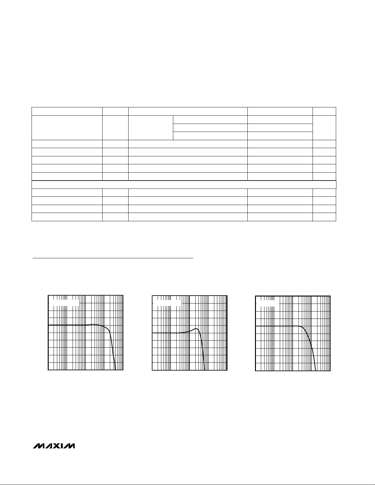
Typical Operating Characteristics
(VCC= +5V; VEE= 0; SHDN ≥ 4V; RL= 150Ω to VCC/2; VCM= 1.5V; A
VCL
= +1V/V (MAX4310/MAX4311/MAX4312), A
VCL
= +2V/V
(MAX4313/MAX4314/MAX4315); T
A
= +25°C; unless otherwise noted.)
4
-6
100k 10M 100M1M 1G
MAX4310
SMALL-SIGNAL GAIN vs. FREQUENCY
-4
MAX4310-01
FREQUENCY (Hz)
GAIN (dB)
-2
0
2
3
1
-1
-3
-5
V
OUT
= 100mVp-p
0.5
-0.5
100k 10M 100M1M 1G
MAX4310
GAIN FLATNESS vs. FREQUENCY
-0.3
MAX4310/15 toc02
FREQUENCY (Hz)
GAIN FLATNESS (dB)
-0.1
0.1
0.3
0.4
0.2
0
-0.2
-0.4
V
OUT
= 100mVp-p
4
-6
100k 10M 100M1M 1G
MAX4310
LARGE-SIGNAL GAIN vs. FREQUENCY
-4
MAX4310/15-03
FREQUENCY (Hz)
GAIN (dB)
-2
0
2
3
1
-1
-3
-5
V
OUT
= 2Vp-p
AC ELECTRICAL CHARACTERISTICS (continued)
(VCC= +5V; VEE= 0; SHDN ≥ 4V; RL= 150Ω; VCM= 1.5V; A
VCL
= +1V/V (MAX4310/MAX4311/MAX4312), A
VCL
= +2V/V
(MAX4313/MAX4314/MAX4315); T
A
= +25°C; unless otherwise noted.)
Page 6
-0.8
1 100010010
MAX4311
GAIN FLATNESS vs. FREQUENCY
-0.4
-0.6
-0.7
0
-0.2
0.2
-0.3
-0.5
0.1
-0.1
MAX4310/15 toc05
FREQUENCY (MHz)
GAIN FLATNESS (dB)
V
OUT
= 100mVp-p
-8
1 100010010
MAX4311
SMALL-SIGNAL GAIN vs. FREQUENCY
-4
-6
-7
0
-2
2
-3
-5
1
-1
MAX4311 toc04
FREQUENCY (MHz)
GAIN (dB)
V
OUT
= 100mVp-p
-0.8
1 100010010
MAX4312
GAIN FLATNESS vs. FREQUENCY
-0.4
-0.6
-0.7
0
-0.2
0.2
-0.3
-0.5
0.1
-0.1
MAX4310/15 toc08
FREQUENCY (MHz)
GAIN FLATNESS (dB)
V
OUT
= 100mVp-p
-8
1 100010010
MAX4312
SMALL-SIGNAL GAIN vs. FREQUENCY
-4
-6
-7
0
-2
2
-3
-5
1
-1
MAX4310/15 toc07
FREQUENCY (MHz)
GAIN (dB)
V
OUT
= 100mVp-p
-8
1 100010010
MAX4311
LARGE-SIGNAL GAIN vs. FREQUENCY
-4
-6
-7
0
-2
2
-3
-5
1
-1
MAX4311 toc06
FREQUENCY (MHz)
GAIN (dB)
V
OUT
= 2Vp-p
-8
1 100010010
MAX4312
LARGE-SIGNAL GAIN vs. FREQUENCY
-4
-6
-7
0
-2
2
-3
-5
1
-1
MAX4310/15 toc09
FREQUENCY (MHz)
GAIN (dB)
V
OUT
= 2Vp-p
4
-6
100k 10M 100M1M 1G
MAX4313
SMALL-SIGNAL GAIN vs. FREQUENCY
-4
MAX4310/15-toc10
FREQUENCY (Hz)
GAIN (dB)
-2
0
2
3
1
-1
-3
-5
V
OUT
= 100mVp-p
0.5
-0.5
100k 10M 100M1M 1G
MAX4313
GAIN FLATNESS vs. FREQUENCY
-0.3
MAX4310/15-toc11
FREQUENCY (Hz)
GAIN FLATNESS (dB)
-0.1
0.1
0.3
0.4
0.2
0
-0.2
-0.4
V
OUT
= 100mVp-p
4
-6
100k 10M 100M1M 1G
MAX4313
LARGE-SIGNAL GAIN vs. FREQUENCY
-4
MAX4310/15-toc12
FREQUENCY (Hz)
GAIN (dB)
-2
0
2
3
1
-1
-3
-5
V
OUT
= 2Vp-p
MAX4310–MAX4315
High-Speed, Low-Power, Single-Supply,
Multichannel, Video Multiplexer-Amplifiers
6 _______________________________________________________________________________________
Typical Operating Characteristics (continued)
(VCC= +5V; VEE= 0; SHDN ≥ 4V; RL= 150Ω to VCC/2; VCM= 1.5V; A
VCL
= +1V/V (MAX4310/MAX4311/MAX4312), A
VCL
= +2V/V
(MAX4313/MAX4314/MAX4315); T
A
= +25°C; unless otherwise noted.)
Page 7

-30
-100
100k 100M10M1M
MAX4310/MAX4311/MAX4312
HARMONIC DISTORTION vs. FREQUENCY
-70
-90
-40
-60
-20
-80
-50
MAX4310/15 toc19
FREQUENCY (Hz)
HARMONIC DISTORTION (dBc)
V
OUT
= 2Vp-p
2ND HARMONIC
3RD HARMONIC
-30
-100
100k 100M10M1M
MAX4313/MAX4314/MAX4315
HARMONIC DISTORTION vs. FREQUENCY
-70
-90
-40
-60
-20
-80
-50
MAX4310/15-20
FREQUENCY (Hz)
HARMONIC DISTORTION (dBc)
V
OUT
= 2Vp-p
2ND HARMONIC
3RD HARMONIC
0
-100
100k 10M 100M1M 1G
POWER-SUPPLY REJECTION
vs. FREQUENCY
-80
MAX4310/15-21
FREQUENCY (Hz)
POWER-SUPPLY REJECTION (dB)
-60
-40
-20
-10
-30
-50
-70
-90
MAX4310–MAX4315
High-Speed, Low-Power, Single-Supply,
Multichannel, Video Multiplexer-Amplifiers
_______________________________________________________________________________________
7
-8
1 100010010
MAX4314
SMALL-SIGNAL GAIN vs. FREQUENCY
-4
-6
-7
0
-2
2
-3
-5
1
-1
MAX4310/15 toc13
FREQUENCY (MHz)
GAIN (dB)
V
OUT
= 100mVp-p
-0.8
1 100010010
MAX4314
GAIN FLATNESS vs. FREQUENCY
-0.4
-0.6
-0.7
0
-0.2
0.2
-0.3
-0.5
0.1
-0.1
MAX4310/15 toc14
FREQUENCY (MHz)
GAIN FLATNESS (dB)
V
OUT
= 100mVp-p
-8
1 100010010
MAX4314
LARGE-SIGNAL GAIN vs. FREQUENCY
-4
-6
-7
0
-2
2
-3
-5
1
-1
MAX4310/15 toc15
FREQUENCY (MHz)
GAIN (dB)
V
OUT
= 2Vp-p
-8
1 100010010
MAX4315
SMALL-SIGNAL GAIN vs. FREQUENCY
-4
-6
-7
0
-2
2
-3
-5
1
-1
MAX4310/15 toc16
FREQUENCY (MHz)
GAIN (dB)
V
OUT
= 100mVp-p
-0.8
1 100010010
MAX4315
GAIN FLATNESS vs. FREQUENCY
-0.4
-0.6
-0.7
0
-0.2
0.2
-0.3
-0.5
0.1
-0.1
MAX4310/15 toc17
FREQUENCY (MHz)
GAIN FLATNESS (dB)
V
OUT
= 100mVp-p
-8
1 100010010
MAX4315
LARGE-SIGNAL GAIN vs. FREQUENCY
-4
-6
-7
0
-2
2
-3
-5
1
-1
MAX4310/15 toc18
FREQUENCY (MHz)
GAIN (dB)
V
OUT
= 2Vp-p
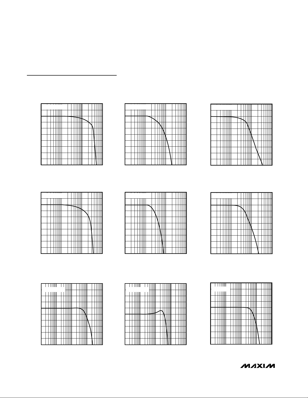
Typical Operating Characteristics (continued)
(VCC= +5V; VEE= 0; SHDN ≥ 4V; RL= 150Ω to VCC/2; VCM= 1.5V; A
VCL
= +1V/V (MAX4310/MAX4311/MAX4312), A
VCL
= +2V/V
(MAX4313/MAX4314/MAX4315); T
A
= +25°C; unless otherwise noted.)
Page 8

MAX4310–MAX4315
High-Speed, Low-Power, Single-Supply,
Multichannel, Video Multiplexer-Amplifiers
8 _______________________________________________________________________________________
0
-100
10k 100k 10M 100M1M 1G
MAX4310/MAX4311/MAX4312
COMMON-MODE REJECTION vs. FREQUENCY
-80
MAX4310/15-toc22
FREQUENCY (Hz)
COMMON-MODE REJECTION (dB)
-60
-40
-20
-10
-30
-50
-70
-90
-10
-110
100k 10M 100M1M 1G
OFF-ISOLATION vs. FREQUENCY
-90
MAX4310/15-toc23
FREQUENCY (Hz)
ISOLATION (dB)
-70
-50
-30
-20
-40
-60
-80
-100
50
-150
0.1 10 1001 1000
MAX4310/MAX4313
All-HOSTILE CROSSTALK vs. FREQUENCY
-110
MAX4310/15-toc24
FREQUENCY (MHz)
CROSSTALK (dB)
-70
-30
10
30
-10
-50
-90
-130
0.1 101 100 1000
MAX4312/MAX4315
ALL-HOSTILE CROSSTALK vs. FREQUENCY
MAX4310/15 toc25
FREQUENCY (MHz)
CROSSTALK (dB)
50
30
10
-10
-150
-110
-130
-30
-50
-70
-90
100
10
10 10k 100k 1M100 1k 10M
VOLTAGE-NOISE DENSITY vs.
FREQUENCY (INPUT REFERRED)
MAX4310/15 toc28a
FREQUENCY (Hz)
VOLTAGE-NOISE DENSITY (nV/√Hz)
0.1 101 100 1000
MAX4311/MAX4314
ALL-HOSTILE CROSSTALK vs. FREQUENCY
MAX4310/15 toc26
FREQUENCY (MHz)
CROSSTALK (dB)
50
30
10
-10
-150
-110
-130
-30
-50
-70
-90
100
0.01
100k 10M 100M1M 1G
OUTPUT IMPEDANCE vs. FREQUENCY
0.1
MAX4310/15-toc27
FREQUENCY (Hz)
OUTPUT IMPEDANCE (Ω)
10
1
100
1
10 10k 100k 1M100 1k 10M
CURRENT-NOISE DENSITY vs.
FREQUENCY (INPUT REFERRED)
10
MAX4310/15 toc29
FREQUENCY (Hz)
CURRENT-NOISE DENSITY (pA/√Hz)
IN
(1V/div)
OUT
(1V/div)
MAX4310
LARGE-SIGNAL PULSE RESPONSE
MAX4310/15 toc30
10ns/div
Typical Operating Characteristics (continued)
(VCC= +5V; VEE= 0; SHDN ≥ 4V; RL= 150Ω to VCC/2; VCM= 1.5V; A
VCL
= +1V/V (MAX4310/MAX4311/MAX4312), A
VCL
= +2V/V
(MAX4313/MAX4314/MAX4315); T
A
= +25°C; unless otherwise noted.)
Page 9

MAX4310–MAX4315
High-Speed, Low-Power, Single-Supply,
Multichannel, Video Multiplexer-Amplifiers
_______________________________________________________________________________________
9
IN
(1V/div)
OUT
(1V/div)
MAX4311
LARGE-SIGNAL PULSE RESPONSE
MAX4310/15-toc33
10ns/div
MAX4312
LARGE-SIGNAL PULSE RESPONSE
MAX43110/15 toc32
10ns/div
IN
(1V/div)
OUT
(1V/div)
IN
(500mV/div)
OUT
(1V/div)
MAX4313
LARGE-SIGNAL PULSE RESPONSE
MAX4310/15-toc33
10ns/div
IN
(500mV/div)
V
OUT
(1V/div)
MAX4314
LARGE-SIGNAL PULSE RESPONSE
MAX4310/15-toc33
10ns/div
MAX4311
SMALL-SIGNAL PULSE RESPONSE
MAX4310/15 toc37a
10ns/div
IN
(50mV/div)
OUT
(50mV/div)
MAX4315
LARGE-SIGNAL PULSE RESPONSE
MAX4310/15 toc35
10ns/div
IN
(500mV/div)
OUT
(IV/div)
IN
(50mV/div)
OUT
(50mV/div)
MAX4310
SMALL-SIGNAL PULSE RESPONSE
MAX4310/15 toc36
10ns/div
MAX4312
SMALL-SIGNAL PULSE RESPONSE
MAX4310/15 toc38
10ns/div
IN
(50mV/div)
OUT
(50mV/div)
IN
(50mV/div)
OUT
(50mV/div)
MAX4313
SMALL-SIGNAL PULSE RESPONSE
MAX4310/15-toc39
10ns/div
Typical Operating Characteristics (continued)
(VCC= +5V; VEE= 0; SHDN ≥ 4V; RL= 150Ω to VCC/2; VCM= 1.5V; A
VCL
= +1V/V (MAX4310/MAX4311/MAX4312), A
VCL
= +2V/V
(MAX4313/MAX4314/MAX4315); T
A
= +25°C; unless otherwise noted.)
Page 10

MAX4310–MAX4315
High-Speed, Low-Power, Single-Supply,
Multichannel, Video Multiplexer-Amplifiers
10 ______________________________________________________________________________________
MAX4314
SMALL-SIGNAL PULSE RESPONSE
MAX4311 toc
10ns/div
IN
(50mV/div)
OUT
(50mV/div)
MAX4315
SMALL-SIGNAL PULSE RESPONSE
MAX4311 toc
10ns/div
IN
(50mV/div)
OUT
(50mV/div)
IN
(50mV/div)
OUT
(50mV/div)
MAX4310
SMALL-SIGNAL PULSE RESPONSE
(C
L
= 10pF)
MAX4310/15-toc42
10ns/div
IN
(50mV/div)
OUT
(50mV/div)
MAX4313
SMALL-SIGNAL PULSE RESPONSE
(C
L
= 22pF)
MAX431015-toc45
10ns/div
IN
(50mV/div)
OUT
(50mV/div)
MAX4310
SMALL-SIGNAL PULSE RESPONSE
(C
L
= 22pF)
MAX4310-TOC22
10ns/div
IN
(50mV/div)
OUT
(50mV/div)
MAX4313
SMALL-SIGNAL PULSE RESPONSE
(C
L
= 10pF)
MAX4310/15-toc44
10ns/div
A0
(2.5V/div)
OUT
(10mV/div)
CHANNEL-SWITCHING TRANSIENT
MAX4310/15 toc46
20ns/div
SHDN
(2.0V/div)
OUT
(1V/div)
SHUTDOWN RESPONSE TIME
MAX4310-TOC27
100ns/div
Typical Operating Characteristics (continued)
(VCC= +5V; VEE= 0; SHDN ≥ 4V; RL= 150Ω to VCC/2; VCM= 1.5V; A
VCL
= +1V/V (MAX4310/MAX4311/MAX4312), A
VCL
= +2V/V
(MAX4313/MAX4314/MAX4315); T
A
= +25°C; unless otherwise noted.)
Page 11

MAX4310–MAX4315
High-Speed, Low-Power, Single-Supply,
Multichannel, Video Multiplexer-Amplifiers
______________________________________________________________________________________ 11
Pin Description
11 V
EE
136
13
— GND——
14
3, 6,
9
N.C.
3, 6,
8, 9,
11
—
OUT168
FB157
13
—
—
16
15
11 136
—
13 157
14
3, 6,93, 6, 8,
9, 11
—
168
——
13
15
—
16
—
Negative Power Supply.
Ground for single-supply
operation.
Ground
Not connected. Tie to
ground plane for optimal
performance.
Amplifier Output
Amplifier Feedback Input
NAME
1 A11—
—
12
SHDN
142
A2——
4
5 IN054
7
8 IN210—
IN175
V
CC
43
10
— IN4——
—
— IN6——
IN5——
IN312—
— IN7——
FUNCTION
Channel Address Logic
Input 1
Shutdown Input
Channel Address Logic
Input 2
Amplifier Input 0
Amplifier Input 2
Amplifier Input 1
Positive Power Supply
Amplifier Input 4
Amplifier Input 6
Amplifier Input 5
Amplifier Input 3
Amplifier Input 7
MAX4312
SO/
QSOP
MAX4313
SO/
µMAX
MAX4315
SO/
QSOP
QSOPSO
A02
QSOP
2
Channel Address Logic
Input 0
2
14
1
5
7
6
4
9
11
10
8
12
3 21 2 3
SO
1 1—
—
12 142
——
4
5 54
7
8 10—
75
43
10
— ——
—
— ——
——
12—
— ——
MAX4310
SO/
µMAX
1
2
14
1
5
7
6
4
9
11
10
8
12
MAX4311 MAX4314
PIN
Page 12

MAX4310–MAX4315
High-Speed, Low-Power, Single-Supply,
Multichannel, Video Multiplexer-Amplifiers
12 ______________________________________________________________________________________
_______________Detailed Description
The MAX4310/MAX4311/MAX4312 combine 2-channel,
4-channel, or 8-channel multiplexers, respectively, with
an adjustable-gain output amplifier optimized for
closed-loop gains of +1V/V (0dB) or greater. The
MAX4313/MAX4314/MAX4315 combine 2-channel, 4channel, or 8-channel multiplexers, respectively, with a
+2V/V (6dB) fixed-gain amplifier, optimized for driving
back-terminated cables. These devices operate from a
single supply voltage of +4V to +10.5V, or from dual
supplies of ±2V to ±5.25V. The outputs may be placed
in a high-impedance state and the supply current minimized by forcing the SHDN pin low. The input multiplexers feature short 40ns channel-switching times and
small 10mVp-p switching transients. The input capacitance remains constant at 1pF whether the channel is
on or off, providing a predictable input impedance to
the signal source. These devices feature single-supply,
rail-to-rail, voltage-feedback output amplifiers that
achieve up to 540V/µs slew rates and up to 345MHz -3dB
bandwidths. These devices also feature excellent harmonic distortion and differential gain/phase performance.
__________Applications Information
Rail-to-Rail Outputs, Ground-Sensing Input
The input common-mode range extends from the negative supply rail to VCC- 2.7V with excellent commonmode rejection. Beyond this range, multiplexer
switching times may increase and the amplifier output
is a nonlinear function of the input, but does not undergo phase reversal or latchup.
The output swings to within 250mV of VCCand 40mV of
VEEwith a 10kΩ load. With a 150Ω load to ground, the
output swings from 30mV above V
EE
to within 730mV of
the supply rail. Local feedback around the output stage
ensures low open-loop output impedance to reduce
gain sensitivity to load variations. This feedback also
produces demand-driven bias current to the output
transistors for ±95mA drive capability while constraining total supply current to only 6.1mA.
Feedback and Gain Resistor Selection
(MAX4310/MAX4311/MAX4312)
Select the MAX4310/MAX4311/MAX4312 gain-setting
feedback (RF) and input (RG) resistors to fit your application. Large resistor values increase voltage noise and
interact with the amplifier’s input and PC board capacitance. This can generate undesirable poles and zeros,
and can decrease bandwidth or cause oscillations. For
example, a noninverting gain of +2V/V configuration (R
F
= RG) using 1kΩ resistors, combined with 2pF of input
capacitance and 1pF of PC board capacitance, causes
a pole at 159MHz. Since this pole is within the amplifier
bandwidth, it jeopardizes stability. Reducing the 1kΩ
resistors to 100Ω extends the pole frequency to
1.59GHz, but could limit output swing by adding 200Ω in
parallel with the amplifier’s load resistor.
Table 1 shows suggested RFand RGvalues for the
MAX4310/MAX4311/MAX4312 when operating in the
noninverting configuration (shown in Figure 1). These
values provide optimal AC response using surfacemount resistors and good layout techniques, as discussed in the
Layout and Power-Supply Bypassing
section.
Stray capacitance at the FB pin causes feedback resis-
tor decoupling and produces peaking in the frequencyresponse curve. Keep the capacitance at FB as low as
possible by using surface-mount resistors and by
avoiding the use of a ground plane beneath or beside
these resistors and the FB pin. Some capacitance is
unavoidable; if necessary, its effects can be neutralized
by adjusting RF. Use 1% resistors to maintain consistency over a wide range of production lots.
MAX4310
R
T
75Ω
8OUT
7FB
IN0
IN1
4
5
1
A0
R
T
75Ω
R
G
R
F
75Ω CABLE
R
T
75Ω
R
T
75Ω
75Ω CABLE
75Ω CABLE
Figure 1. MAX4310 Noninverting Gain Configuration
Table 1. Bandwidth and Gain with
Suggested Gain-Setting Resistors
(MAX4310/MAX4311/MAX4312)
GAIN
(V/V)
GAIN
(dB)
R
F
(Ω)
R
G
(Ω)
-3dB BW
(MHz)
0.1dB BW
(MHz)
80
280
500
∞
500
0
6
01
2
5 14 500 120 420
210565002010
30
60
Page 13

MAX4310–MAX4315
High-Speed, Low-Power, Single-Supply,
Multichannel, Video Multiplexer-Amplifiers
______________________________________________________________________________________ 13
Low-Power Shutdown Mode
All parts feature a low-power shutdown mode that is
activated by driving the SHDN input low. Placing the
amplifier in shutdown mode reduces the quiescent supply current to 560µA and places the output into a highimpedance state, typically 35kΩ. By tying the outputs
of several devices together and disabling all but one of
the paralleled amplifiers’ outputs, multiple devices may
be paralleled to construct larger switch matrices.
For MAX4310/MAX4311/MAX4312 application circuits
operating with a closed-loop gain of +2V/V or greater,
consider the external-feedback network impedance of
all devices used in the mux application when calculating the total load on the output amplifier of the active
device. The MAX4313/MAX4314/MAX4315 have a fixed
gain of +2V/V that is internally set with two 500Ω thin-
film resistors. The impedance of the internal feedback
resistors must be taken into account when operating
multiple MAX4313/MAX4314/MAX4315s in large multiplexer applications.
For normal operation, drive SHDN high. If the shutdown
function is not used, connect SHDN to V
CC
.
Layout and Power-Supply Bypassing
The MAX4310–MAX4315 have very high bandwidths
and consequently require careful board layout, including the possible use of constant-impedance microstrip
or stripline techniques.
To realize the full AC performance of these high-speed
amplifiers, pay careful attention to power-supply
bypassing and board layout. The PC board should
have at least two layers: a signal and power layer on
one side, and a large, low-impedance ground plane on
the other side. The ground plane should be as free of
voids as possible, with one exception: the feedback
(FB) should have as low a capacitance to ground as
possible. Therefore, layers that do not incorporate a
signal or power trace should not have a ground plane.
Whether or not a constant-impedance board is used, it
is best to observe the following guidelines when
designing the board:
1) Do not use wire-wrapped boards (they are too
inductive) or breadboards (they are too capacitive).
2) Do not use IC sockets; they increase parasitic
capacitance and inductance.
3) Keep signal lines as short and straight as possible.
Do not make 90° turns; round all corners.
4) Observe high-frequency bypassing techniques to
maintain the amplifier’s accuracy and stability.
5) Use surface-mount components. They generally
have shorter bodies and lower parasitic reactance,
yielding better high-frequency performance than
through-hole components.
OUT
IN-
SHDN, A0, A1, A2
IN+
10k
LOGIC INPUT
MAX431_
Figure 3. Circuit to Reduce Logic-Low Input Current
0
-10
0 50 100 150 300 350 500
-7
-8
-1
LOGIC-LOW THRESHOLD (mV ABOVE V
EE
)
INPUT CURRENT (µA)
200 250 400 450
-3
-5
-9
-2
-4
-6
Figure 4. Logic-Low Input Current vs. VILwith 10kΩSeries
Resistor
20
-160
0 50 100 150 300 350 500
-100
-120
0
LOGIC-LOW THRESHOLD (mV ABOVE V
EE
)
INPUT CURRENT (µA)
200 250 400 450
-60
-140
-20
-40
-80
Figure 2. Logic-Low Input Current vs. V
IL
(SHDN, A0, A1, A2)
Page 14

MAX4310–MAX4315
High-Speed, Low-Power, Single-Supply,
Multichannel, Video Multiplexer-Amplifiers
14 ______________________________________________________________________________________
The bypass capacitors should include a 100nF, ceramic surface-mount capacitor between each supply pin
and the ground plane, located as close to the package
as possible. Optionally, place a 10µF tantalum capacitor at the power-supply pins’ point of entry to the PC
board to ensure the integrity of incoming supplies. The
power-supply trace should lead directly from the tantalum capacitor to the VCCand VEEpins. To minimize
parasitic inductance, keep PC traces short and use surface-mount components.
If input termination resistors and output back-termination
resistors are used, they should be surface-mount types,
and should be placed as close to the IC pins as possible.
Video Line Driver
The MAX4310–MAX4315 are well-suited to drive coaxial
transmission lines when the cable is terminated at both
ends, as shown in Figure 5. Cable frequency response
can cause variations in the signal’s flatness.
MAX4313
R
T
75Ω
8OUT
IN0
IN1
4
5
17
GND
A0
R
T
75Ω
500Ω
500Ω
75Ω CABLE
OUT
R
T
75Ω
R
T
75Ω
75Ω CABLE
75Ω CABLE
Figure 5. Video Line Driver
100M 1G
-6
4
3
2
0
-1
-2
-3
-4
-5
1
100k 1M 10M
MAX4310-FIG06
FREQUENCY (Hz)
GAIN (dB)
V
OUT
= 100mVp-p
10pF LOAD
5pF LOAD
15pF LOAD
Figure 6. Small-Signal Gain vs. Frequency with Capacitive
Load and No Isolation Resistor
MAX4313
R
ISO
8OUT
IN0
IN1
4
5
17
GND
A0
R
L
C
L
500Ω
500Ω
R
T
75Ω
R
T
75Ω
75Ω CABLE
75Ω CABLE
Figure 7. Using an Isolation Resistor (R
ISO
) for High
Capacitive Loads
10
15
20
25
30
0 50 100 150 200 250
MAX4310-FIG08
CAPACITIVE LOAD (pF)
ISOLATION RESISTANCE R
ISO
(Ω)
Figure 8. Optimal Isolation Resistance vs. Capacitive Load
100M 1G
-6
4
3
2
0
-1
-2
-3
-4
-5
1
100k 1M 10M
MAX4310-FIG09
FREQUENCY (Hz)
GAIN (dB)
V
OUT
= 100mVp-p
47pF LOAD
90pF LOAD
120pF LOAD
Figure 9. Small-Signal Gain vs. Frequency with Load
Capacitance and 27
Ω
Isolation Resistor
Page 15

MAX4310–MAX4315
High-Speed, Low-Power, Single-Supply,
Multichannel, Video Multiplexer-Amplifiers
______________________________________________________________________________________ 15
Driving Capacitive Loads
A correctly terminated transmission line is purely resistive and presents no capacitive load to the amplifier.
Reactive loads decrease phase margin and may produce excessive ringing and oscillation (see
Typical
Operating Characteristics
).
Another concern when driving capacitive loads originates from the amplifier’s output impedance, which
appears inductive at high frequencies. This inductance
forms an L-C resonant circuit with the capacitive load,
which causes peaking in the frequency response and
degrades the amplifier’s phase margin.
Although the MAX4310–MAX4315 are optimized for AC
performance and are not designed to drive highly capacitive loads, they are capable of driving up to 20pF without
oscillations. However, some peaking may occur in the frequency domain (Figure 6). To drive larger capacitive
loads or to reduce ringing, add an isolation resistor
between the amplifier’s output and the load (Figure 7).
The value of R
ISO
depends on the circuit’s gain and the
capacitive load (Figure 8). Figure 9 shows the
MAX4310–MAX4315 frequency response with the isolation resistor and a capacitive load. With higher capacitive values, bandwidth is dominated by the RC network
formed by R
ISO
and CL; the bandwidth of the amplifier
itself is much higher. Also note that the isolation resistor
forms a divider that decreases the voltage delivered to
the load.
Figure 10. High-Speed EV Board Layout—Component Side
Figure 11. High-Speed EV Board Layout—Solder Side
1 0 1
001
CHANNEL SELECTED A2
SHDN
1 0 3
201
0
0
A1
1
1
0 X None, High-Z OutputX
1 1 4
1 1 6
511
0
1
0
1 1 71
1
0
A0
1
0
X
0
0
1
1
1 — 1
0—1
CHANNEL SELECTED A2
SHDN
1 — 3
2—1
—
—
A1
1
1
0 — None, High-Z Output—
1
0
A0
1
0
X
1 — 1
0—1
CHANNEL SELECTED A2
SHDN
0
0
A1
0 — None, High-Z OutputX
1
0
A0
X
MAX4310/MAX4313
MAX4311/MAX4314
MAX4312/MAX4315
Table 2. Input Control Logic
Page 16

MAX4310–MAX4315
Digital Interface
The multiplexer architecture of the MAX4310–MAX4315
ensures that no two input channels are ever connected
together. Channel selection is accomplished by applying a binary code to channel address inputs. The
address decoder selects input channels, as shown in
Table 2. All digital inputs are CMOS compatible.
High-Speed Evaluation Board
Figures 10 and 11 show the evaluation board and present a suggested layout for the circuits. This board was
developed using the techniques described in the
Layout and Power-Supply Bypassing
section of this
data sheet. The smallest available surface-mount resistors were used for feedback and back-termination to
minimize their distance from the part, reducing the
capacitance associated with longer lead lengths.
SMA connectors were used for best high-frequency
performance. Inputs and outputs do not match a 75Ω
line, but this does not affect performance since distances are extremely short. However, in applications
that require lead lengths greater than one-quarter of the
wavelength of the highest frequency of interest, use
constant-impedance traces.
Fully assembled evaluation boards are available for the
MAX4313 in an SO package.
High-Speed, Low-Power, Single-Supply,
Multichannel, Video Multiplexer-Amplifiers
16 ______________________________________________________________________________________
MAX4313
0.1µF
75Ω
8OUT
3
V
CC
+4V TO +10.5V
IN1
IN0
5
4
1627
A0
75Ω
500Ω
GND
V
EE
SHDN
500Ω
VIDEO
OUTPUT
75Ω CABLE
Typical Operating Circuit
Chip Information
TRANSISTOR COUNT: 156
Page 17

MAX4310–MAX4315
High-Speed, Low-Power, Single-Supply,
Multichannel, Video Multiplexer-Amplifiers
______________________________________________________________________________________ 17
TOP VIEW
N.C. = NOT INTERNALLY CONNECTED. TIE TO GROUND PLANE
FOR OPTIMAL PERFORMANCE.
A2
A1
A0
N.C.
V
CC
IN0
IN1
N.C.
500Ω
MAX4314
16
15
14
13
12
11
10
9
1
2
3
4
5
6
7
8
MUX
QSOP
OUT
GND
SHDN
V
EE
IN3
N.C.
IN2
N.C.
500Ω
OUT
GND
SHDN
V
EE
V
CC
N.C.
A0
A1
MAX4314
IN3
N.C.
IN2IN1
N.C.
IN0
SO
500Ω
14
13
12
11
10
9
8
1
2
3
4
5
6
7
MUX
500Ω
MAX4313
V
EE
IN1
IN0
OUT
GND
SHDN
V
CC
A0
SO/µMAX
500Ω
8
7
6
5
1
2
3
4
MUX
500Ω
MAX4315
SO/QSOP
500Ω
16
15
14
13
12
11
10
9
1
2
3
4
5
6
7
8
A2
MUX
A1
A0
IN1
V
CC
IN0
IN2
IN3
OUT
GND
SHDN
V
EE
IN7
IN6
IN5
IN4
500Ω
MAX4312
SO/QSOP
16
15
14
13
12
11
10
9
1
2
3
4
5
6
7
8
A2
MUX
A1
A0
IN1
V
CC
IN0
IN2
IN3
OUT
FB
SHDN
V
EE
IN7
IN6
IN5
IN4
MAX4311
QSOP
16
15
14
13
12
11
10
9
1
2
3
4
5
6
7
8
A1
MUX
A0
N.C.
N.C.
V
CC
IN0
IN1
N.C.
OUT
FB
SHDN
V
EE
IN3
N.C.
IN2
N.C.
MAX4311
SO
14
13
12
11
10
9
8
1
2
3
4
5
6
7
A1
MUX
A0
N.C.
N.C.
V
CC
IN0
IN1
OUT
FB
SHDN
V
EE
IN3
N.C.
IN2
MAX4310
V
EE
IN1IN0
1
2
87OUT
FBSHDN
V
CC
A0
SO/µMAX
3
4
6
5
-
+
MUX
Pin Configurations
Page 18

MAX4310–MAX4315
High-Speed, Low-Power, Single-Supply,
Multichannel, Video Multiplexer-Amplifiers
18 ______________________________________________________________________________________
8LUMAXD.EPS
Package Information
Page 19

MAX4310–MAX4315
High-Speed, Low-Power, Single-Supply,
Multichannel, Video Multiplexer-Amplifiers
______________________________________________________________________________________ 19
Package Information (continued)
QSOP.EPS
Page 20

MAX4310–MAX4315
High-Speed, Low-Power, Single-Supply,
Multichannel, Video Multiplexer-Amplifiers
Package Information (continued)
SOICN.EPS
20 ______________________________________________________________________________________
 Loading...