

Page 1
For free samples & the latest literature: http://www.maxim-ic.com, or phone 1-800-998-8800.
For small orders, phone 1-800-835-8769.
MAX4291/MAX4292/MAX4294
Ultra-Small, +1.8V, µPower,
Rail-to-Rail I/O Op Amps
________________________________________________________________ Maxim Integrated Products 1
V
EE
OUTIN-
15V
CC
IN+
SC70-5/SOT23-5
TOP VIEW
2
34
V
EE
OUTB
OUTA
INB-
INB+
V
CC
INA+
INA-
µMAX/SO
1
2
8
7
3
4
6
5
MAX4292
MAX4291
19-1612; Rev 0; 3/00
Pin Configurations
Rail-to-Rail is a registered trademark of Nippon Motorola, Ltd.
8 µMAX
5 SOT23-5
5 SC70-5
PIN-
PACKAGE
TEMP. RANGE
-40°C to +85°C
-40°C to +85°C
-40°C to +85°C
MAX4292EUA*
MAX4291EUK-T
MAX4291EXK-T
PART
Ordering Information
Selector Guide
—
ADML
AAD
TOP
MARK
14 TSSOP
14 SO
8 SO -40°C to +85°C
-40°C to +85°C
-40°C to +85°CMAX4294EUD*
MAX4294ESD*
MAX4292ESA*
—
—
—
Pin Configurations continued at end of data sheet.
14-pin SO/TSSOP
8-pin µMAX/SO
5-pin SC70/SOT23
PIN-PACKAGE
AMPLIFIERS
PER PACKAGE
1
2
4MAX4294
MAX4292
MAX4291
PART
General Description
The MAX4291/MAX4292/MAX4294 family of micropower operational amplifiers operates from a +1.8V to
+5.5V single supply or ±0.9V to ±2.75V dual supplies
and has Rail-to-Rail®input/output capabilities. These
amplifiers provide a 500kHz gain-bandwidth product
and 120dB open-loop voltage gain while using only
100µA of supply current per amplifier. The combination
of low input offset voltage (±400µV) and high-open-loop
gain makes them suitable for low-power/low-voltage
high-precision applications.
The MAX4291/MAX4292/MAX4294 have an input common-mode range that extends to each supply rail, and
their outputs typically swing within 20mV of the rails with
a 2kΩ load. Although the minimum operating voltage is
specified at +1.8V, these devices typically operate down
to +1.5V. The combination of ultra-low-voltage operation,
rail-to-rail inputs/output, and low-power consumption
makes these devices ideal for any portable/two-cell battery-powered system.
The single MAX4291 is offered in an ultra-small 5-pin
SC70 package and the dual MAX4292 is offered in a
space-saving 8-pin µMAX package.
Applications
2-Cell Battery-Operated Systems
Portable Electronic Equipment
Battery-Powered Instrumentation
Digital Scales
Strain Gauges
Sensor Amplifiers
Cellular Phones
Features
♦ Ultra-Low Voltage Operation—Guaranteed Down
to +1.8V
♦ 100µA Supply Current per Amplifier
♦ 500kHz Gain-Bandwidth Product
♦ 120dB Open-Loop Voltage Gain (R
L
= 100kΩ)
♦ 0.017% THD + Noise at 1kHz
♦ Rail-to-Rail Input Common-Mode Range
♦ Rail-to-Rail Output Drives 2kΩ Load
♦ No Phase Reversal for Overdriven Inputs
♦ Unity-Gain Stable for Capacitive Loads up to 100pF
♦ 400µV Input Offset Voltage
♦ Single Available in Ultra-Small 5-Pin SC70
Dual Available in Space-Saving 8-Pin µMAX
*Future product—contact factory for availability.
Page 2
MAX4291/MAX4292/MAX4294
Ultra-Small, +1.8V, µPower,
Rail-to-Rail I/O Op Amps
2 _______________________________________________________________________________________
ABSOLUTE MAXIMUM RATINGS
ELECTRICAL CHARACTERISTICS
(VCC= +1.8V to +5.5V, VEE= VCM= 0, V
OUT
= V
CC
/ 2, RL= 100kΩ connected to V
CC
/ 2, TA= +25°C, unless otherwise noted.)
(Note 1)
Stresses beyond those listed under “Absolute Maximum Ratings” may cause permanent damage to the device. These are stress ratings only, and functional
operation of the device at these or any other conditions beyond those indicated in the operational sections of the specifications is not implied. Exposure to
absolute maximum rating conditions for extended periods may affect device reliability.
Supply Voltage (VCCto V
EE)
..................................................+6V
All Other Pins ...................................(V
CC
+ 0.3V) to (VEE- 0.3V)
Output Short-Circuit Duration.....................................Continuous
Continuous Power Dissipation (T
A
= +70°C)
5-Pin SC70 (derate 2.5mW/°C above +70°C) ................200mW
5-Pin SOT23 (derate 7.1mW/°C above +70°C)................571mW
8-Pin µMAX (derate 4.10mW/°C above +70°C)..............330mW
8-Pin SO (derate 5.88mW/°C above +70°C) ..................471mW
14-Pin SO (derate 8.33mW/°C above +70°C) ................667mW
14-Pin TSSOP (derate 6.3mW/°C above +70°C) ............500mW
Operating Temperature Range............................-40°C to +85°C
Junction Temperature ......................................................+150°C
Storage Temperature Range .............................-65°C to +150°C
Lead Temperature (soldering, 10s) .................................+300°C
80 100
80 100
MAX4292ESA, MAX4294ESD
MAX4292EUA, MAX4294EUD
MAX4291EXK, MAX4291EUK
MAX4292ESA, MAX4294ESD
MAX4292EUA, MAX4294EUD
MAX4291EXK, MAX4291EUK
70 90
70 90
Tested for
0 ≤ V
CM
≤
5.0V,
V
CC
= 5.0V
dB
60 90
65 85
65 85
Common-Mode Rejection Ratio CMRR
Tested for
0 ≤ V
CM
≤
1.8V;
VCC= 1.8V
dB
50 80
Power-Supply Rejection Ratio PSRR dB
80 100MAX4291EXK, MAX4291EUK
V
OS
110 225VCC= 5.0V
PARAMETER SYMBOL MIN TYP MAX UNITS
Input Bias Current I
B
±15 ±55 nA
±400 ±1500
±400 ±1500
Input Offset Voltage
±400 ±2500
µV
Input Offset Current I
OS
±1 ±7 nA
Differential Input Resistance R
IN
0.75 MΩ
Input Common-Mode Voltage
Range
V
CM
0V
CC
V
Quiescent Supply Current
(per Amplifier)
Supply Voltage Range V
CC
1.8 5.5 V
I
Q
100 210
µA
CONDITIONS
VCC= 5.0V, 0 ≤ VCM≤ 5.0V
MAX4292ESA, MAX4294ESD
MAX4292EUA, MAX4294EUD
MAX4291EXK, MAX4291EUK
VCC= 5.0V, 0 ≤ VCM≤ 5.0V
|V
IN+
- V
IN-
| < 10mV
Inferred from CMRR test
Inferred from PSRR test
VCC= 1.8V
MAX4292ESA, MAX4294ESD
MAX4292EUA, MAX4294EUD
Page 3
MAX4291/MAX4292/MAX4294
Ultra-Small, +1.8V, µPower,
Rail-to-Rail I/O Op Amps
_______________________________________________________________________________________ 3
ELECTRICAL CHARACTERISTICS
(VCC= +1.8V to +5.5V, VEE= VCM= 0, V
OUT
= V
CC
/ 2, RL= 100kΩ connected to V
CC
/ 2, TA= T
MIN
to T
MAX
, unless otherwise
noted.) (Note 1)
ELECTRICAL CHARACTERISTICS
(VCC= +1.8V to +5.5V, VEE= VCM= 0, V
OUT
= V
CC
/ 2, RL= 100kΩ connected to V
CC
/ 2, TA= +25°C, unless otherwise noted.)
(Note 1)
Channel-to-Channel Isolation
Gain Bandwidth Product
Phase Margin
Gain Margin
Slew Rate
Input Voltage Noise Density
Input Current Noise Density
Capacitive-Load Stability
CH
ISO
GBW
φ
M
G
M
SR
e
n
i
n
Specified at f = 10kHz (MAX4292/MAX4294 only)
f = 10kHz
f = 10kHz
A
VCL
= +1V/V, no sustained oscillations
100
500
65
12
0.2
70
0.05
100 pF
pA/√Hz
nV/√Hz
V/µs
dB
degrees
kHz
dB
mA20Sourcing or sinkingI
OUT(SC)
Output Short-Circuit Current
Output Voltage Swing Low V
OL
Specified as
|V
EE
– VOL|
RL= 2kΩ to V
CC
/ 2
RL= 100kΩ to V
CC
/ 2
18 40
315
mV
mV
15 40
220
RL= 2kΩ to V
CC
/ 2
RL= 100kΩ to V
CC
/ 2
Specified as
|V
CC
– VOH|
V
OH
Output Voltage Swing High
Large-Signal Voltage Gain A
V
VCC= 5.0V
VCC= 1.8V
RL= 100kΩ,
0.015V ≤ V
OUT
≤ VCC- 0.015V
RL= 2kΩ,
0.1V ≤ V
OUT
≤ VCC- 0.1V
RL= 100kΩ,
0.015V ≤ V
OUT
≤ VCC- 0.015V
RL= 2kΩ,
0.1V ≤ V
OUT
≤ VCC- 0.1V
80 120
80 130
80 110
80 120
dB
UNITSMIN TYP MAXCONDITIONSSYMBOLPARAMETER
270VCC= 5.0V
PARAMETER SYMBOL MIN TYP MAX UNITS
±1500
±1500
Input Offset Voltage V
OS
±3000
µV
Quiescent Supply Current
(per Amplifier)
Supply Voltage Range V
CC
1.8 5.5 V
I
Q
240
µA
CONDITIONS
MAX4292ESA, MAX4294ESD
MAX4292EUA, MAX4294EUD
MAX4291EXK, MAX4291EUK
Inferred from PSRR test
VCC= 1.8V
Page 4
MAX4292ESA, MAX4294ESD
Ultra-Small, +1.8V, µPower,
Rail-to-Rail I/O Op Amps
4 _______________________________________________________________________________________
Note 1: All devices are 100% tested at TA= +25°C. All temperature limits are guaranteed by design.
VCC= 5.0V, 0 ≤ VCM≤ 5.0V
VCC= 5.0V, 0 ≤ VCM≤ 5.0V
Specified as
|VEE– VOL|
Specified as
|VCC– VOH|
Inferred from CMRR test
Tested for
0 ≤ VCM≤ 1.8V,
V
CC
= 1.8V
MAX4291EXK, MAX4291EUK
VCC= 1.8V
CONDITIONS
nA±10I
OS
Input Offset Current
nA±80I
B
µV/°C1.2TCV
OS
Input Offset Voltage Drift
Input Bias Current
mV
15
V
OL
Output Voltage Swing Low
mV
20
V
OH
Output Voltage Swing High
V0V
CC
V
CM
Input Common-Mode Voltage
Range
dB
50
CMRRCommon-Mode Rejection Ratio
dB
78
PSRRPower-Supply Rejection Ratio
dB
80
A
V
Large-Signal Voltage Gain
UNITSMIN TYP MAXSYMBOLPARAMETER
MAX4291EXK, MAX4291EUK
MAX4292ESA, MAX4294ESD
MAX4292EUA, MAX4294EUD
MAX4291EXK, MAX4291EUK
MAX4292ESA, MAX4294ESD
MAX4292EUA, MAX4294EUD
Tested for
0 ≤ VCM≤ 5.0V,
VCC= 5.0V
65
65
60
60
60
dB
80
80
RL= 100kΩ,
0.015V ≤ V
OUT
≤ VCC- 0.015V
RL= 2kΩ,
0.1V ≤ V
OUT
≤ VCC- 0.1V
RL= 100kΩ,
0.015V ≤ V
OUT
≤ VCC- 0.015V
RL= 2kΩ,
0.1V ≤ V
OUT
≤ VCC- 0.1V
VCC= 5.0V
80
80
80
RL= 100kΩ to V
CC
/ 2
RL= 100kΩ to V
CC
/ 2
RL= 2kΩ to V
CC
/ 2
RL= 2kΩ to V
CC
/ 2
40
40
ELECTRICAL CHARACTERISTICS
(VCC= +1.8V to +5.5V, VEE= VCM= 0, V
OUT
= V
CC
/ 2, RL= 100kΩ connected to V
CC
/ 2, TA= T
MIN
to T
MAX
, unless otherwise
noted.) (Note 1)
MAX4291/MAX4292/MAX4294
MAX4292ESA, MAX4294ESD
MAX4292EUA, MAX4294EUD
Page 5
Ultra-Small, +1.8V, µPower,
Rail-to-Rail I/O Op Amps
MAX4291/MAX4292/MAX4294
_______________________________________________________________________________________ 5
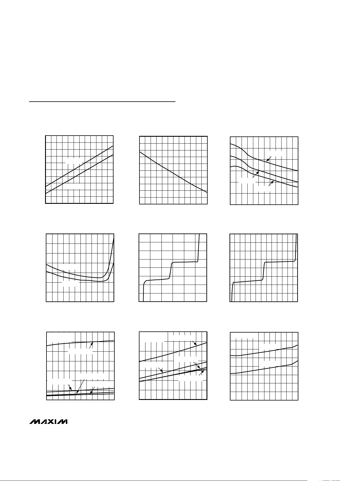
1.0
1.2
1.1
1.5
1.4
1.3
1.6
1.7
1.9
1.8
2.0
-55 -25 -10-40
520355065 80 95 110
MINIMUM OPERATING VOLTAGE
vs. TEMPERATURE (PSRR ≥80dB)
MAX4291 toc02
TEMPERATURE (°C)
MINIMUM OPERATING VOLTAGE (V)
125
-900
-600
-750
-300
-450
-150
0
-55 -25 -10 5-40 20 5035 65 80 95 110125
INPUT OFFSET VOLTAGE
vs. TEMPERATURE
MAX4291 toc03
TEMPERATURE (°C)
INPUT OFFSET VOLTAGE (µV)
VCC = 5.5V
VCC = 1.8V
VCC = 2.4V
0
10
5
20
15
30
25
35
-55 -25 -10 5-40 20 35 50 65 80 95 110 125
INPUT BIAS CURRENT
vs. TEMPERATURE
MAX4291 toc04
TEMPERATURE (°C)
INPUT BIAS CURRENT (nA)
VCC = 5.5V
VCC = 1.8V
-40
-30
-20
-10
0
10
20
30
40
-0.5 0.50 1.0 1.5 2.0 2.5
INPUT BIAS CURRENT vs. COMMON-MODE
VOLTAGE (V
CC
= 1.8V)
MAX4291 toc05
COMMON-MODE VOLTAGE (V)
INPUT BIAS CURRENT (nA)
-40
-10
-20
-30
0
10
30
20
40
-0.5 0.5 1.5 2.5 3.5
4.5 5.5
INPUT BIAS CURRENT vs. COMMON-MODE
VOLTAGE (V
CC
= 5.5V)
MAX4291 toc06
COMMON-MODE VOLTAGE (V)
INPUT BIAS CURRENT (nA)
0.0
1.0
0.5
2.0
1.5
3.0
2.5
3.5
-55 -25 -10 5-40 20 35 50 65 80 95 110 125
OUTPUT VOLTAGE SWING vs.
TEMPERATURE (R
L
= 100kΩ to V
CC
/ 2)
MAX4291 toc07
TEMPERATURE (°C)
OUTPUT VOLTAGE SWING (mV)
VOL (VCC = 5.5V)
V
OH
= VCC - V
OUT
V
OL
= V
OUT
- V
EE
VOH (VCC = 5.5V)
VOH (VCC = 1.8V)
VOL (VCC = 1.8V)
0
10
5
20
15
30
25
35
-55 -25 -10 5-40 20 35 50 65 80 95 110 125
OUTPUT VOLTAGE SWING vs.
TEMPERATURE (R
L
= 2kΩ to V
CC
/ 2)
MAX4291 toc08
TEMPERATURE (°C)
OUTPUT VOLTAGE SWING (mV)
VOL (VCC = 5.5V)
V
OH
= VCC - V
OUT
V
OL
= V
OUT
- V
EE
VOH (VCC = 5.5V)
VOH (VCC = 1.8V)
VOL (VCC = 1.8V)
-105
-90
-95
-100
-85
-80
-70
-75
-65
-55 -25 -10-40 5 203550658095110125
COMMON-MODE REJECTION
RATIO vs. TEMPERATURE
MAX4291 toc09
TEMPERATURE (°C)
CMRR (dB)
VCC = 5.5V
VCC = 1.8V
0 ≤ V
CM
≤ V
CC
Typical Operating Characteristics
(VCC= +2.4V, VEE= VCM= 0, V
OUT
= V
CC
/ 2, no load, TA= +25°C, unless otherwise noted.)
60
80
70
110
100
90
120
130
150
140
160
-55 -25 -10-40
520355065 80 95 110
SUPPLY CURRENT PER AMPLIFIER
vs. TEMPERATURE
MAX4291 toc01
TEMPERATURE (°C)
SUPPLY CURRENT (µA)
125
VCC = 5.5V
VCC = 1.8V
Page 6

MAX4291/MAX4292/MAX4294
Ultra-Small, +1.8V, µPower,
Rail-to-Rail I/O Op Amps
6 _______________________________________________________________________________________
Typical Operating Characteristics (continued)
(VCC= +2.4V, VEE= VCM= 0, V
OUT
= V
CC
/ 2, no load, TA= +25°C, unless otherwise noted.)
50
70
60
80
110
120
100
90
130
0 100 150 200 25050 300 350 400 450 500
OPEN-LOOP GAIN vs. OUTPUT SWING LOW
(V
CC
= +1.8V, RL CONNECTED TO VCC)
MAX4291 toc10
VOL (mV)
GAIN (dB)
RL = 2kΩ
RL = 1kΩ
50
70
60
90
80
110
100
120
0 200100 300 40050 250150 350 450 500
OPEN-LOOP GAIN vs. OUTPUT SWING HIGH
(V
CC
= +1.8V, RL CONNECTED TO VEE)
MAX4291 toc11
VOH (mV)
GAIN (dB)
RL = 2kΩ
RL = 1kΩ
50
70
60
80
110
120
100
90
130
0 100 150 200 25050 300 350 400 450 500
OPEN-LOOP GAIN vs. OUTPUT SWING LOW
(V
CC
= +5.5V, RL CONNECTED TO VCC)
MAX4191 toc12
VOL (mV)
GAIN (dB)
RL = 2kΩ
RL = 1kΩ
50
70
60
80
110
120
100
90
130
0 100 150 200 25050 300 350 400 450 500
OPEN-LOOP GAIN vs. OUTPUT SWING HIGH
(V
CC
= +5.5V, RL CONNECTED TO VEE)
MAX4191 toc13
VOH (mV)
GAIN (dB)
RL = 2kΩ
RL = 1kΩ
50
80
70
60
90
100
120
110
130
-55 -25 -10-40 5 203550658095110125
OPEN-LOOP GAIN vs. TEMPERATURE
MAX4291 toc14
TEMPERATURE (°C)
OPEN-LOOP GAIN (dB)
RL = 2kΩ TO V
CC
RL = 2kΩ TO V
EE
RL = 1kΩ TO V
CC
RL = 1kΩ TO V
EE
VCC = 5.5V
60
-40
0.1 1 10 100 1000
GAIN AND PHASE vs. FREQUENCY
(C
L
= 0)
-20
MAX4291 toc15
FREQUENCY (kHz)
GAIN (dB)
0
20
40
30
10
-10
-30
50
AV = +1000V/V
180
144
108
72
36
0
-36
-72
-108
-144
-180
PHASE (DEGREES)
60
-40
0.1 1 10 100 1000
GAIN AND PHASE vs. FREQUENCY
(C
L
= 100pF)
-20
MAX4291 toc16
FREQUENCY (kHz)
GAIN (dB)
0
20
40
30
10
-10
-30
50
AV = +1000V/V
180
144
108
72
36
0
-36
-72
-108
-144
-180
PHASE (DEGREES)
1
0.01
0.01 10 100
0.1
FREQUENCY (kHz)
THD + NOISE (%)
10.1
TOTAL HARMONIC DISTORTION
PLUS NOISE vs. FREQUENCY
VCC = +5.5V
VCC = +1.8V
MAX4291 toc18
RL = 2kΩ
A
v
= +1V/V
(NONINVERTING
CONFIGURATION)
Page 7

MAX4291/MAX4292/MAX4294
Ultra-Small, +1.8V, µPower,
Rail-to-Rail I/O Op Amps
_______________________________________________________________________________________ 7
0.01
0.1
10
1
100
0 23451 678910
LOAD RESISTOR vs. CAPACITIVE LOAD
MAX4291 toc19
CAPACITIVE LOAD (nF)
LOAD RESISTOR (kΩ)
I
OUT
> 20mA
V
CC
= 2.4V
I
OUT
> 20mA
V
CC
= 5.5V
VCC = 5.5V
VCC = 2.4V
10% OVERSHOOT
A
V
= +1V/V
(NONINVERTING CONFIGURATION)
OUT
IN
0
100mV
0
100mV
1µs/div
SMALL-SIGNAL TRANSIENT RESPONSE
(NONINVERTING CONFIGURATION)
MAX4291 toc20
VCC = +2.5V
V
EE
= -2.5V
V
CM
= 0
OUT
IN
0
100mV
0
100mV
1µs/div
SMALL-SIGNAL TRANSIENT RESPONSE
(INVERTING CONFIGURATION)
MAX4291 toc21
VCC = +2.5V
V
EE
= -2.5V
V
CM
= 0
OUT
IN
-2V
+2V
-2V
+2V
10µs/div
LARGE-SIGNAL TRANSIENT RESPONSE
(NONINVERTING CONFIGURATION)
MAX4291 toc22
VCC = +2.5V
V
EE
= -2.5V
V
CM
= 0
OUT
IN
-2V
+2V
-2V
+2V
10µs/div
LARGE-SIGNAL TRANSIENT RESPONSE
(INVERTING CONFIGURATION)
MAX4291 toc23
VCC = +2.5V
V
EE
= -2.5V
V
CM
= 0
0
1000
500
2000
1500
2500
3000
010155 202530
SUPPLY CURRENT vs. SINK CURRENT
MAX4291/2/4-24
SINK CURRENT (mA)
SUPPLY CURRENT (µA)
VCC = 5.5V
VCC = 2.4V
VCC = 1.8V
0
60
45
30
15
105
90
75
120
135
150
0105152025
SUPPLY CURRENT vs. SOURCE CURRENT
MAX4291/2/4-25
SOURCE CURRENT (mA)
SUPPLY CURRENT (µA)
VCC = 5.5V
VCC = 1.8V
VCC = 2.4V
Typical Operating Characteristics (continued)
(VCC= +2.4V, VEE= VCM= 0, V
OUT
= V
CC
/ 2, no load, TA= +25°C, unless otherwise noted.)
Page 8

Detailed Description
Rail-to-Rail Input Stage
The MAX4291/MAX4292/MAX4294 have rail-to-rail
inputs and output stages that are specifically designed
for low-voltage, single-supply operation. The input
stage consists of separate NPN and PNP differential
stages, which operate together to provide a commonmode range extending to both supply rails. The
crossover region of these two pairs occurs halfway
between VCCand VEE. The input offset voltage is typically ±400µV. Low operating supply voltage, low supply current, rail-to-rail common-mode input range, and
rail-to-rail outputs make this family of operational amplifiers (op amps) an excellent choice for precision or
general-purpose, low-voltage, battery-powered systems.
Since the input stage consists of NPN and PNP pairs,
the input bias current changes polarity as the commonmode voltage passes through the crossover region.
Match the effective impedance seen by each input to
reduce the offset error caused by input bias currents
flowing through external source impedances (Figures
1a and 1b).
The combination of high source impedance plus input
capacitance (amplifier input capacitance plus stray
capacitance) creates a parasitic pole that produces an
underdamped signal response. Reducing input capacitance or placing a small capacitor across the feedback
resistor improves response in this case.
MAX4291/MAX4292/MAX4294
Ultra-Small, +1.8V, µPower,
Rail-to-Rail I/O Op Amps
8 _______________________________________________________________________________________
Pin Description
R3
IN
R3 = R1 R2
R1 R2
MAX4291
MAX4292
MAX4294
R3
R3 = R1 R2
R1 R2
MAX4291
MAX4292
MAX4294
IN
Figure 1a. Minimizing Offset Error Due to Input Bias Current
(Noninverting)
Figure 1b. Minimizing Offset Error Due to Input Bias Current
(Inverting)
PIN
NAME
IN+
V
EE
OUTA, OUTB
V
CC
OUT
IN-
INC+, IND+
INC-, IND-
OUTC, OUTD
INA+, INB+
INA-, INB-
MAX4294
–
11
1, 7
4
–
–
10, 12
9, 13
8, 14
3, 5
2, 6
FUNCTION
MAX4291
MAX4292
1 – Noninverting Input
2 4 Negative Supply. Connect to ground for single-supply operation.
– 1, 7 Outputs for Amplifiers A and B
5 8 Positive Supply
4 – Amplifier Output
3 – Inverting Input
– – Noninverting Inputs to Amplifiers C and D
– – Inverting Inputs to Amplifiers C and D
– – Outputs for Amplifiers C and D
– 3, 5 Noninverting Inputs to Amplifiers A and B
– 2, 6 Inverting Inputs to Amplifiers A and B
Page 9

The MAX4291/MAX4292/MAX4294 family’s inputs are
protected from large differential input voltages by internal 10.6kΩ series resistors and back-to-back triplediode stacks across the inputs (Figure 2). For
differential input voltages (much less than 1.8V), input
resistance is typically 0.75MΩ. For differential input
voltages greater than 1.8V, input resistance is around
21.2kΩ, and the input bias current can be approximated by the following equation:
In the region where the differential input voltage
approaches 1.8V, the input resistance decreases exponentially from 0.75MΩ to 21.2kΩ as the diode block
begins to conduct. Conversely, the bias current
increases with the same curve.
In unity-gain configuration, high slew rate input signals
may capacitively couple to the output through the triplediode stacks.
Rail-to-Rail Output Stage
The MAX4291/MAX4292/MAX4294 output stage can
drive up to a 2kΩ load and still swing to within 20mV of
the rails. Figure 3 shows the output voltage swing of a
MAX4291 configured as a unity-gain buffer, powered
from a ±2.5V supply. The output for this setup typically
swings from (VEE+ 3mV) to (VCC- 2mV) with a 100kΩ
load.
Applications Information
Power-Supply Considerations
The MAX4291/MAX4292/MAX4294 operate from a single +1.8V to +5.5V supply (or dual ±0.9V to ±2.75V
supplies) and consume only 100µA of supply current
per amplifier. A high power-supply rejection ratio of
80dB allows the amplifiers to be powered directly off a
decaying battery voltage, simplifying design and
extending battery life.
The MAX4291/MAX4292/MAX4294 are ideally suited for
use with most battery-powered systems. Table 1 lists a
variety of typical battery types showing voltage when
fresh, voltage at end-of-life, capacity, and approximate
operating time from a MAX4291 (assuming nominal
conditions).
I
(V - 1.8V)
21.2k
BIAS
DIFF
=
Ω
MAX4291/MAX4292/MAX4294
Ultra-Small, +1.8V, µPower,
Rail-to-Rail I/O Op Amps
_______________________________________________________________________________________ 9
Table 1. MAX4291 Characteristics with Typical Battery Systems
750Yes
Nickel-Cadmium
(2 cells)
1000Yes
Lithium-Ion
(1 cell)
1000Yes
Nickel-MetalHydride (2 cells)
2000NoAlkaline (2 cells)
BATTERY TYPE
CAPACITY, AA SIZE
(mA-h)
2.4
3.5
2.4
3.0
1.8
2.7
1.8
1.8
V
END-OF-LIFE
(V)
V
FRESH
(V)
RECHARGE-
ABLE
7500
10,000
10,000
20,000
MAX4291
OPERATING TIME IN
NORMAL MODE
(h)
OUT
2.5V/div
IN
2.5V/div
0
0
20µs/div
VCC = +2.5V, V
EE
= -2.5V
Figure 3. Rail-to-Rail Input/Output Voltage Range
10.6k
10.6k
IN-
IN+
Figure 2. Input Protection Circuit
Page 10

MAX4291/MAX4292/MAX4294
Although the amplifiers are fully guaranteed over temperature for operation down to a +1.8V single supply,
even lower voltage operation is possible in practice.
Figures 4 and 5 show the offset voltage and supply current as a function of supply voltage and temperature.
Load-Driving Capability
The MAX4291/MAX4292/MAX4294 are fully guaranteed
over temperature and supply voltage range to drive a
maximum resistive load of 2kΩ to VCC/2, although
heavier loads can be driven in many applications. The
rail-to-rail output stage of the amplifier can be modeled
as a current source when driving the load toward VCC,
and as a current sink when driving the load toward VEE.
The limit of this current source/sink varies with supply
voltage, ambient temperature, and lot-to-lot variations
of the units.
Figures 6a and 6b show the typical current source and
sink capabilities of the MAX4291/MAX4292/MAX4294
family as a function of supply voltage and ambient temperature. The contours on the graph depict the output
current value, based on driving the output voltage to
within 50mV, 100mV, and 200mV of either power-supply rail.
For example, a MAX4291 running from a single +1.8V
supply, operating at TA= +25°C can source 3.5mA to
within 100mV of VCCand is capable of driving a 485Ω
load resistor to VEE:
The same application can drive a 220kΩ load resistor
when terminated in VCC/2 (+0.9V in this case).
R
(1.8V 0.1V)
3.5mA
485 to V
LEE
=
−=
Ω
Ultra-Small, +1.8V, µPower,
Rail-to-Rail I/O Op Amps
10 ______________________________________________________________________________________
SUPPLY VOLTAGE (V)
-700
-600
-650
-550
-500
-450
032.521 1.50.5 3.5 4 4.5 5 5.5
OFFSET VOLTAGE vs. SUPPLY VOLTAGE
OFFSET VOLTAGE (µV)
TA = +25°C
TA = -40°C
TA = +85°C
VCM = VCC/
2
Figure 4. Offset Voltage vs. Supply Voltage
0
60
20
40
80
100
120
140
0 2 2.5 310.5 1.5 3.5 4.5 54 5.5
SUPPLY CURRENT vs. SUPPLY VOLTAGE
SUPPLY VOLTAGE (V)
SUPPLY CURRENT (µA)
TA = +85°C
TA = -40°C
TA = +25°C
Figure 5. Supply Current vs. Supply Voltage
0
15
5
10
20
25
30
-55 5 20 35-25-40 -10 50 80 1109565 125
OUTPUT SOURCE CURRENT
vs. TEMPERATURE
TEMPERATURE (°C)
OUTPUT SOURCE CURRENT (mA)
VOH = V
CC
- V
OUT
VCC = 5.5V
V
OH
= 200mV
VCC = 5.5V
V
OH
= 50mV
VCC = 1.8V
V
OH
= 100mV
VCC = 1.8V
V
OH
= 200mV
VCC = 5.5V
V
OH
= 100mV
VCC = 1.8V
V
OH
= 50mV
Figure 6a. Output Source Current vs. Temperature
VOL = V
OUT
- V
EE
0
10
2
4
6
8
12
14
16
18
-55 5 20 35-25-40 -10 50 80 1109565 125
OUTPUT SINK CURRENT
vs. TEMPERATURE
TEMPERATURE (°C)
OUTPUT SINK CURRENT (mA)
VCC = 1.8V
V
OL
= 200mV
VCC = 1.8V
V
OL
= 50mV
VCC = 5.5V
V
OL
= 200mV
VCC = 5.5V
V
OL
= 100mV
VCC = 1.8V
V
OL
= 100mV
VCC = 5.5V
V
OL
= 50mV
Figure 6b. Output Sink Current vs. Temperature
Page 11

Driving Capacitive Loads
The MAX4291/MAX4292/MAX4294 are unity-gain stable
for loads up to 100pF (see the Load Resistor vs.
Capacitive Load graph in the Typical Operating
Characteristics). Applications that require greater
capacitive drive capability should use an isolation
resistor between the output and the capacitive load
(Figure 7). Note that this alternative results in a loss of
gain accuracy because R
ISO
forms a voltage divider
with the load resistor.
Power-Supply Bypassing and Layout
The MAX4291/MAX4292/MAX4294 family operates from
either a single +1.8V to +5.5V supply or dual ±0.9V to
±2.75V supplies. For single-supply operation, bypass
the power supply with a 100nF capacitor to VEE(in this
case GND). For dual-supply operation, both the V
CC
and the VEEsupplies should be bypassed to ground
with separate 100nF capacitors.
Good PC board layout techniques optimize performance by decreasing the amount of stray capacitance
at the op amp’s inputs and output. To decrease stray
capacitance, minimize trace lengths and widths by
placing external components as close as possible to
the op amp. Surface-mount components are an excellent choice.
Using the MAX4291/MAX4292/MAX4294
as Comparators
Although optimized for use as operational amplifiers,
the MAX4291/MAX4292/MAX4294 can also be used as
rail-to-rail I/O comparators. Typical propagation delay
depends on the input overdrive voltage, as shown in
Figure 8. External hysteresis can be used to minimize
the risk of output oscillation. The positive feedback circuit, shown in Figure 9, causes the input threshold to
change when the output voltage changes state. The
two thresholds create a hysteresis band that can be
calculated by the following equations:
When the output of the comparator is low, the supply
current increases. The output stage has biasing circuitry to monitor the output current. When the amplifier is
MAX4291/MAX4292/MAX4294
Ultra-Small, +1.8V, µPower,
Rail-to-Rail I/O Op Amps
______________________________________________________________________________________ 11
R
ISO
C
L
R
L
MAX4240
MAX4241
MAX4242
MAX4243
MAX4244
AV =
R
L
≈ 1
R
L
+ R
ISO
OUT
IN
Figure 7a. Using a Resistor to Isolate a Capacitive Load from
the Op Amp
OUT
IN
0
100mV
0
100mV
10µs/div
VCC = +2.4V, R
L
= 2kΩ TO V
EE, CL
= 1000pF
Figure 7b. Pulse Response Without Isolating Resistor
OUT
IN
0
100mV
0
100mV
10µs/div
VCC = +2.4V, R
L
= 2kΩ TO V
EE
, CL = 1000pF, R
ISO
= 100Ω
Figure 7c. Pulse Response with Isolating Resistor (100 Ω)
V V V
V 1
R1
R2
R1
R
V
V V
R1
R
V
HYST HI LO
HI
HYST
REF
LO HI
HYST
CC
=−
=+ +
=−
Page 12

MAX4291/MAX4292/MAX4294
used as a comparator, the output stage is overdriven
and the current through the biasing circuitry increases
to maximum. For the MAX4291, typical supply currents
increase to 1.5mA with V
CC
= 1.8V and to 9mA when
V
CC
= 5.0V (Figure 10).
Using the MAX4291/MAX4292/MAX4294
as Low-Power Current Monitors
The MAX4291/MAX4292/MAX4294 are ideal for applications powered from a two-cell battery stack. Figure
11 shows an application circuit in which the MAX4291
is used for monitoring the current of a two-cell battery
stack. In this circuit, a current load is applied, and the
voltage drop at the battery terminal is sensed.
The voltage on the load side of the battery stack is
equal to the voltage at the emitter of Q1 due to the
feedback loop containing the op amp. As the load current increases, the voltage drop across R1 and R2
increases. Thus, R2 provides a fraction of the load current (set by the ratio of R1 and R2) that flows into the
emitter of the PNP transistor. Neglecting PNP base current, this current flows into R3, producing a ground-referenced voltage proportional to the load current. To
minimize errors, scale R1 to give a voltage drop that is
large enough in comparison to the op amp’s VOS.
Calculate the output voltage of the application using
the following equation:
For a 1V output and a current load of 50mA, the choice
of resistors can be R1 = 2Ω, R2 = 100kΩ, and R3 =
1MΩ.
VI
R1
R2
R3
OUT LOAD
=×
×
Ultra-Small, +1.8V, µPower,
Rail-to-Rail I/O Op Amps
12 ______________________________________________________________________________________
06090
20 30
10
40 50 8070 100
PROPAGATION DELAY
vs. INPUT OVERDRIVE
VOD (mV)
10
100
1000
t
PD
(µs)
tPD+, VCC = 5.5V
tPD-, VCC = 5.5V
tPD+, VCC = 1.8V
tPD-, VCC = 1.8V
Figure 8. Propagation Delay vs. Input Overdrive
R2
R1
V
SIG
OUTPUT
INPUT
V
OH
V
OL
V
EE
= GND
V
CC
V
OUT
R
HYST
V
EE
= GND
MAX4291
MAX4292
MAX4294
HYSTERESIS
V
LO
V
HI
V
REF
Figure 9. Hysteresis Comparator Circuit
0
6
2
4
8
10
12
0 2 2.5 310.5 1.5 3.5 4.5 54 5.5
MAXIMUM SUPPLY CURRENT
vs. SUPPLY VOLTAGE
SUPPLY VOLTAGE (V)
MAXIMUM SUPPLY CURRENT (mA)
COMPARATOR CONFIGURATION
V
IN+
= (VIN-) - 100mV
Figure 10. Maximum Supply Current vs. Supply Voltage
Page 13

MAX4291/MAX4292/MAX4294
Ultra-Small, +1.8V, µPower,
Rail-to-Rail I/O Op Amps
______________________________________________________________________________________ 13
R1
I
LOAD
R2
V
CC
V
EE
R3
V
OUT
Q1
MAX4291
Figure 11. Current Monitor for a 2-Cell Battery Stack
TOP VIEW
OUTA
OUTB
OUTD
OUTC
V
CC
INA+
INB+
IND+
INC+
INA-
INB-
IND-
INC-
V
EE
1
5
6
7
MAX4294
TSSOP/SO
2
3
4
14
10
9
8
13
12
11
Pin Configurations (continued)
Chip Information
MAX4291 TRANSISTOR COUNT: 149
MAX4292 TRANSISTOR COUNT: 356
MAX4294 TRANSISTOR COUNT: 747
Page 14

MAX4291/MAX4292/MAX4294
Ultra-Small, +1.8V, µPower,
Rail-to-Rail I/O Op Amps
14 ______________________________________________________________________________________
Package Information
SC70, 5L.EPS
SOT5L.EPS
Page 15

MAX4291/MAX4292/MAX4294
Ultra-Small, +1.8V, µPower,
Rail-to-Rail I/O Op Amps
______________________________________________________________________________________ 15
Package Information (continued)
8LUMAXD.EPS
SOICN.EPS
Note: The MAX4292 does not have an exposed pad.
Page 16

MAX4291/MAX4292/MAX4294
Ultra-Small, +1.8V, µPower,
Rail-to-Rail I/O Op Amps
Maxim cannot assume responsibility for use of any circuitry other than circuitry entirely embodied in a Maxim product. No circuit patent licenses are
implied. Maxim reserves the right to change the circuitry and specifications without notice at any time.
16 ____________________Maxim Integrated Products, 120 San Gabriel Drive, Sunnyvale, CA 94086 408-737-7600
© 2000 Maxim Integrated Products Printed USA is a registered trademark of Maxim Integrated Products.
Package Information (continued)
TSSOP.EPS
Note: The MAX4294 does not have an exposed pad.
 Loading...