

Page 1
General Description
The MAX4238/MAX4239 are low-noise, low-drift, ultrahigh precision amplifiers that offer near-zero DC offset
and drift through the use of autocorrelating zeroing techniques. This method constantly measures and compensates the input offset, eliminating drift over time and
temperature and the effect of 1/f noise. Both devices feature rail-to-rail outputs, operate from a single 2.7V to 5.5V
supply, and consume only 600µA. An active-low shutdown mode decreases supply current to 0.1µA.
The MAX4238 is unity-gain stable with a gain-bandwidth product of 1MHz, while the decompensated
MAX4239 is stable with A
V
≥ 10V/V and a GBWP of
6.5MHz. The MAX4238/MAX4239 are available in 8-pin
narrow SO, 6-pin TDFN and SOT23 packages.
Applications
Thermocouples
Strain Gauges
Electronic Scales
Medical Instrumentation
Instrumentation Amplifiers
Features
♦ Ultra-Low, 0.1µV Offset Voltage
2.0µV (max) at +25°C
2.5µV (max) at -40°C to +85°C
3.5µV (max) at -40°C to +125°C
♦ Low 10nV/
o
C Drift
♦ Specified over the -40
o
C to +125oC Automotive
Temperature Range
♦ Low Noise: 1.5µV
P-P
from DC to 10Hz
♦ 150dB A
VOL
, 140dB PSRR, 140dB CMRR
♦ High Gain-Bandwidth Product
1MHz (MAX4238)
6.5MHz (MAX4239)
♦ 0.1µA Shutdown Mode
♦ Rail-to-Rail Output (R
L
= 1kΩ)
♦ Low 600µA Supply Current
♦ Ground-Sensing Input
♦ Single 2.7V to 5.5V Supply Voltage Range
♦ Available in a Space-Saving 6-Pin SOT23 and
TDFN Packages
MAX4238/MAX4239
Ultra-Low Offset/Drift, Low-Noise,
Precision SOT23 Amplifiers
________________________________________________________________ Maxim Integrated Products 1
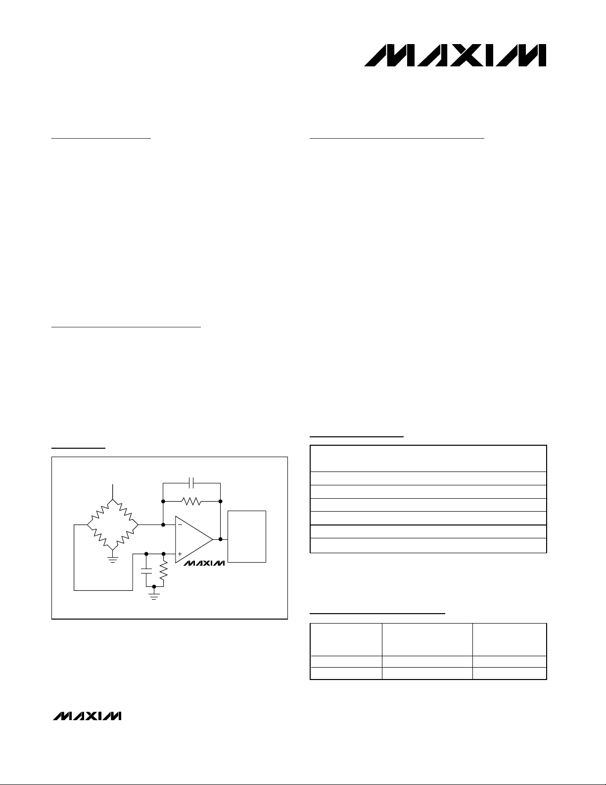
MAX4238/
MAX4239
360Ω
STRAIN GUAGE
18kΩ
18kΩ
AIN
5V
AV = 100
ADC
Typical Application Circuit
19-2424; Rev 2; 5/06
For pricing, delivery, and ordering information, please contact Maxim/Dallas Direct! at
1-888-629-4642, or visit Maxim’s website at www.maxim-ic.com.
Pin Configurations appear at end of data sheet.
Note: All devices are specified over the -40°C to +125°C oper-
ating temperature range.
+Denotes lead-free package.
*EP = Exposed paddle.
Ordering Information
PART
PINPACKAGE
TOP
PKG
CODE
MAX4238AUT-T 6 SOT23-6
AAZZ
U6F-6
MAX4238ASA 8 SO
—
S8-4
MAX4238ATT+T 6 TDFN-EP*
T633-2
MAX4239AUT-T 6 SOT23-6
ABAA
U6F-6
MAX4239ASA 8 SO
—
S8-4
MAX4239ATT+T 6 TDFN-EP*
T633-2
Selector Guide
PART
MINIMUM STABLE
GAIN
GAIN
BANDWIDTH
(MHz)
MAX4238 1V/V 1
MAX4239 10V/V 6.5
MARK
+ANG
+ANH
Page 2
MAX4238/MAX4239
Ultra-Low Offset/Drift, Low-Noise,
Precision SOT23 Amplifiers
2 _______________________________________________________________________________________
ABSOLUTE MAXIMUM RATINGS
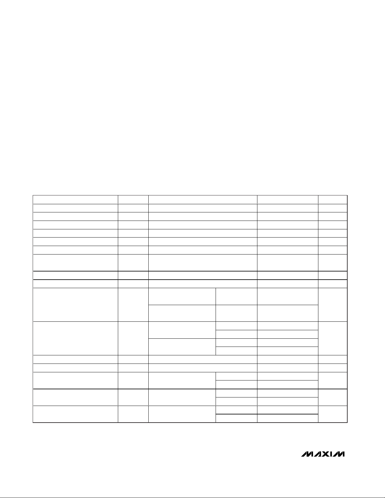
ELECTRICAL CHARACTERISTICS
(2.7V ≤ VCC≤ 5.5V, VCM= GND = 0V, V
OUT
= VCC/2, RL= 10kΩ connected to VCC/2, SHDN = VCC, TA= +25°C,
unless otherwise noted.)
Stresses beyond those listed under “Absolute Maximum Ratings” may cause permanent damage to the device. These are stress ratings only, and functional
operation of the device at these or any other conditions beyond those indicated in the operational sections of the specifications is not implied. Exposure to
absolute maximum rating conditions for extended periods may affect device reliability.
Power-Supply Voltage (VCCto GND).......................................6V
All Other Pins .................................(GND - 0.3V) to (V
CC
+ 0.3V)
Output Short-Circuit Duration
(OUT shorted to V
CC
or GND) ...............................Continuous
Continuous Power Dissipation (T
A
= +70°C)
6-Pin Plastic SOT23
(derate 9.1mW/
°
C above +70°C) ...............................727mW
8-Pin Plastic SO (derate 5.88mW/
°
C above +70°C).....471mW
6-Pin TDFN-EP (derate 18.2mW above +70°C) .........1454mW
Operating Temperature Range ..........................-40
°
C to +125°C
Junction Temperature ......................................................+150
°
C
Storage Temperature Range..............................-65
°
C to +150°C
Lead Temperature (soldering, 10s) .................................+300
°
C
PARAMETER
SYMBOL
CONDITIONS
MIN
TYP
MAX
UNITS
Input Offset Voltage V
OS
(Note 1) 0.1 2 µV
Long-Term Offset Drift 50
nV/1000hr
Input Bias Current I
B
(Note 2) 1 pA
Input Offset Current I
OS
(Note 2) 2 pA
e
nP-P
RS = 100Ω, 0.01Hz to 10Hz 1.5 µV
P-P
Input Voltage-Noise Density e
n
f = 1kHz 30
NV/√Hz
Common-Mode Input
Voltage Range
V
CM
Inferred from CMRR test
GND
V
Common-Mode Rejection Ratio CMRR -0.1V ≤ VCM ≤ VCC - 1.3V (Note 1)
dB
Power-Supply Rejection Ratio PSRR 2.7V ≤ VCC ≤ 5.5V (Note 1)
dB
0.05V ≤ V
OU T
≤ V
C C
- 0.05V
( N ote 1)
R
L
= 10kΩ
Large-Signal Voltage Gain A
VOL
0.1V ≤ V
OUT
≤ VCC - 0.1V
(Note 1)
R
L
= 1kΩ
dB
VCC - V
OH
410
RL = 10kΩ
V
OL
410
VCC - V
OH
35 50
Output Voltage Swing
RL = 1kΩ
V
OL
35 50
mV
Output Short-Circuit Current To either supply 40 mA
Output Leakage Current 0 ≤ V
OUT
≤ VCC, SHDN = GND (Note 2)
1µA
MAX4238
Slew Rate
V
CC
= 5V, CL = 100pF,
V
OUT
= 2V step
MAX4239 1.6
V/µs
MAX4238 1
Gain-Bandwidth Product GBWP
R
L
= 10kΩ, CL = 100pF,
measured at f = 100kHz
MAX4239 6.5
MHz
MAX4238 1
Minimum Stable Closed-Loop
Gain
RL = 10kΩ, CL = 100pF,
phase margin = 60
o
MAX4239 10
V/V
Peak-to-Peak Input Noise Voltage
- 0.1
VOH/V
OL
120 140
120 140
125 150
125 145
0.01
0.35
- 1.3
V
CC
Page 3
MAX4238/MAX4239
Ultra-Low Offset/Drift, Low-Noise,
Precision SOT23 Amplifiers
_______________________________________________________________________________________ 3
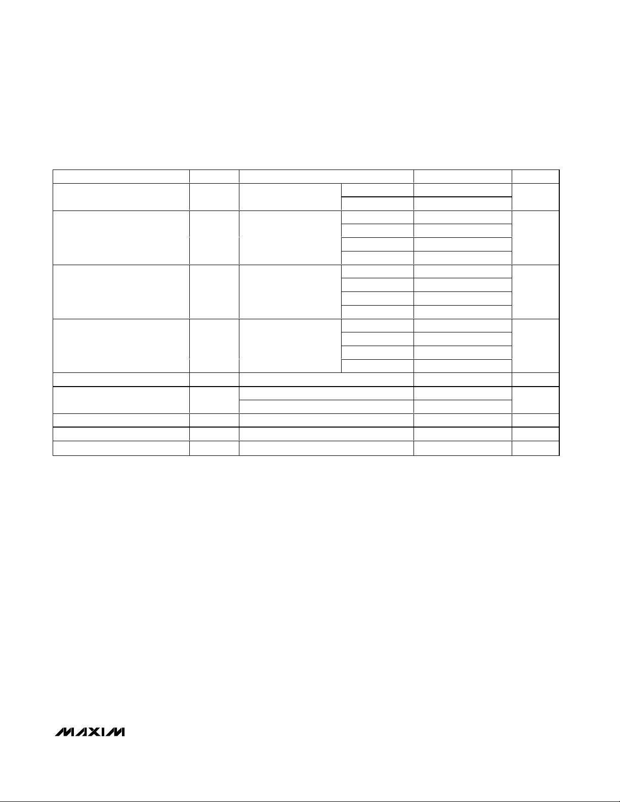
ELECTRICAL CHARACTERISTICS (continued)
(2.7V ≤ VCC≤ 5.5V, VCM= GND = 0V, V
OUT
= VCC/2, RL= 10kΩ connected to VCC/2, SHDN = VCC, TA= +25°C,
unless otherwise noted.)
PARAMETER
SYMBOL
CONDITIONS
MIN
TYP
MAX
UNITS
MAX4238
Maximum Closed-Loop Gain
R
L
= 10kΩ, CL = 100pF,
phase margin = 60
o
MAX4239
V/V
0.1% (10 bit) 0.5
0.025% (12 bit) 1.0
0.006% (14 bit) 1.7
Settling Time -1V step
2.3
ms
0.1% (10 bit) 3.3
0.025% (12 bit) 4.1
0.006% (14 bit) 4.9
Overload Recovery Time
A
V
= 10
(Note 4)
5.7
ms
0.1% (10 bit) 1.8
0.025% (12 bit) 2.6
0.006% (14 bit) 3.4
Startup Time AV = 10
4.3
ms
Supply Voltage Range V
CC
Inferred by PSRR test
V
SHDN = VCC, no load, VCC = 5.5V
Supply Current I
CC
SHDN = GND, VCC = 5.5V 0.1 1
µA
Shutdown Logic-High V
IH
V
Shutdown Logic-Low V
IL
V
Shutdown Input Current 0V ≤ V
SHDN
≤ V
CC
0.1 1 µA
1000
6700
0.0015% (16 bit)
0.0015% (16 bit)
0.0015% (16 bit)
2.7 5.5
600 850
2.2
0.8
Page 4
MAX4238/MAX4239
Ultra-Low Offset/Drift, Low-Noise,
Precision SOT23 Amplifiers
4 _______________________________________________________________________________________
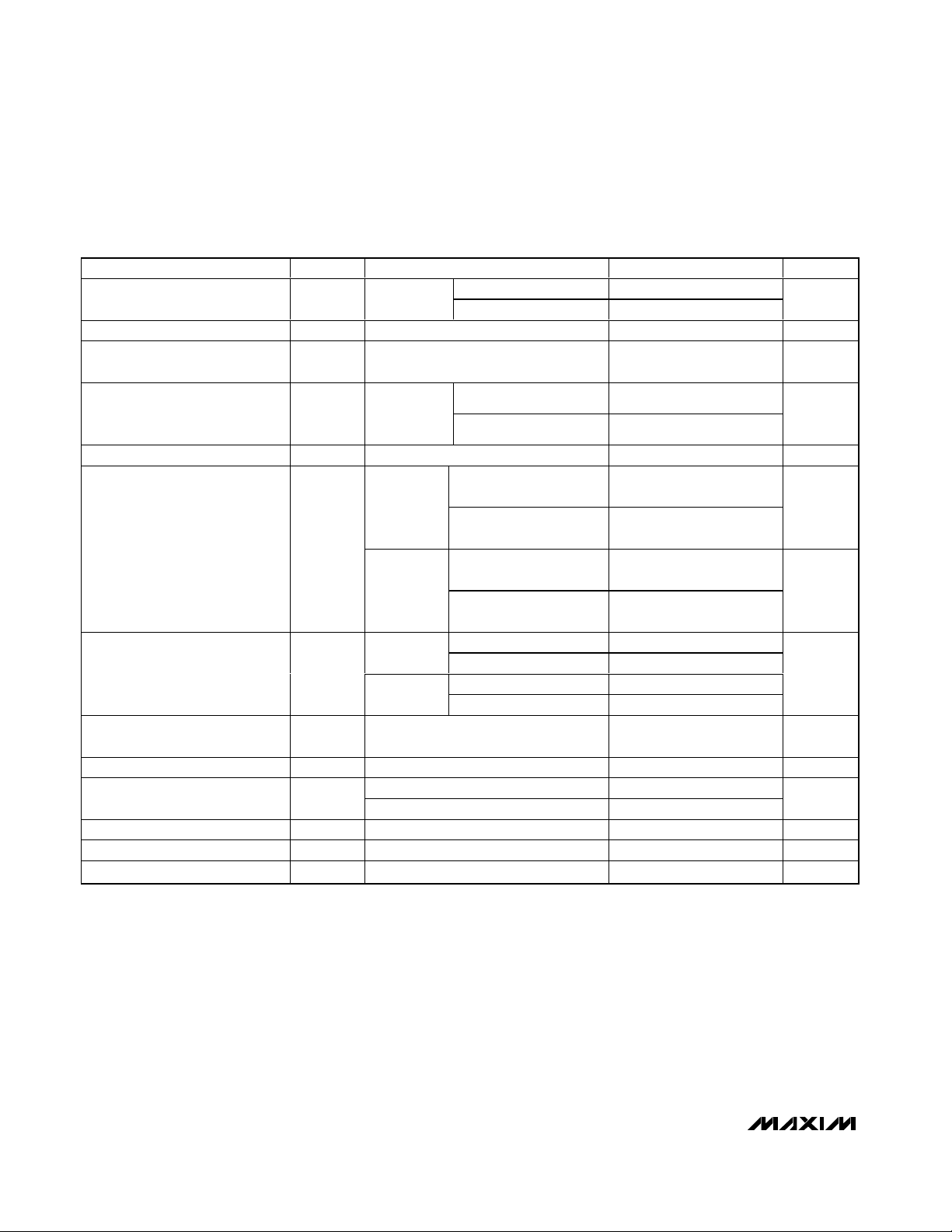
ELECTRICAL CHARACTERISTICS
(2.7V ≤ VCC≤ 5.5V, VCM= GND = 0V, V
OUT
= VCC/2, RL= 10kΩ connected to VCC/2, SHDN = VCC, TA= -40°C to +125°C, unless other-
wise noted.) (Note 5)
PARAMETER
SYMBOL
CONDITIONS MIN
TYP
MAX
UNITS
TA = -40°C to +85°C 2.5
Input Offset Voltage V
OS
(Note 1)
T
A
= -40°C to +125°C 3.5
µV
Input Offset Drift TCV
OS
(Note 1) 10 nV/°C
Common-Mode Input Voltage
Range
V
CM
Inferred from CMRR test
V
TA = -40°C to +85°C 115
Common-Mode Rejection Ratio CMRR
GN D - 0.05V ≤
V
C M
≤ V
C C
TA = -40°C to +125°C 90
dB
Power-Supply Rejection Ratio PSRR 2.7V ≤ VCC ≤ 5.5V (Note 1) 120 dB
TA = -40°C to +85°C 125
RL = 10kΩ,
0.1V ≤ V
OUT
≤ VCC - 0.1V
(Note 1)
T
A
= -40°C to +125°C 95
dB
0.1V ≤ V
OUT
≤ VCC - 0.1V,
T
A
= -40°C to +85°C
120
Large-Signal Voltage Gain A
VOL
RL = 1kΩ
(Note 1)
0.2V ≤ V
OUT
≤ VCC - 0.2V,
T
A
= -40°C to +125°C
80
dB
VCC - V
OH
20
RL = 10kΩ
V
OL
20
VCC - V
OH
100
Output Voltage Swing
RL = 1kΩ
V
OL
100
mV
Output Leakage Current
0V ≤ V
OUT
≤ VCC, SHDN = GND
(Note 3)
2µA
Supply Voltage Range V
CC
Inferred by PSRR test 2.7 5.5 V
SHDN = VCC, no load, VCC = 5.5V 900
Supply Current I
CC
SHDN = GND, VCC = 5.5V 2
µA
Shutdown Logic High V
IH
2.2 V
Shutdown Logic Low V
IL
0.7 V
Shutdown Input Current 0V ≤ V
SHDN
≤ V
CC
2µA
Note 1: Guaranteed by design. Thermocouple and leakage effects preclude measurement of this parameter during production
testing. Devices are screened during production testing to eliminate defective units.
Note 2: IN+ and IN- are gates to CMOS transistors with typical input bias current of 1pA. CMOS leakage is so small that it is
impractical to test and guarantee in production. Devices are screened during production testing to eliminate defective units.
Note 3: Leakage does not include leakage through feedback resistors.
Note 4: Overload recovery time is the time required for the device to recover from saturation when the output has been
driven to either rail.
Note 5: Specifications are 100% tested at T
A
= +25°C, unless otherwise noted. Limits over temperature are guaranteed by design.
GND
- 0.05
1.4V ( N ote 1)
VOH/V
OL
V
- 1.4
CC
Page 5
MAX4238/MAX4239
Ultra-Low Offset/Drift, Low-Noise,
Precision SOT23 Amplifiers
_______________________________________________________________________________________ 5
Typical Operating Characteristics
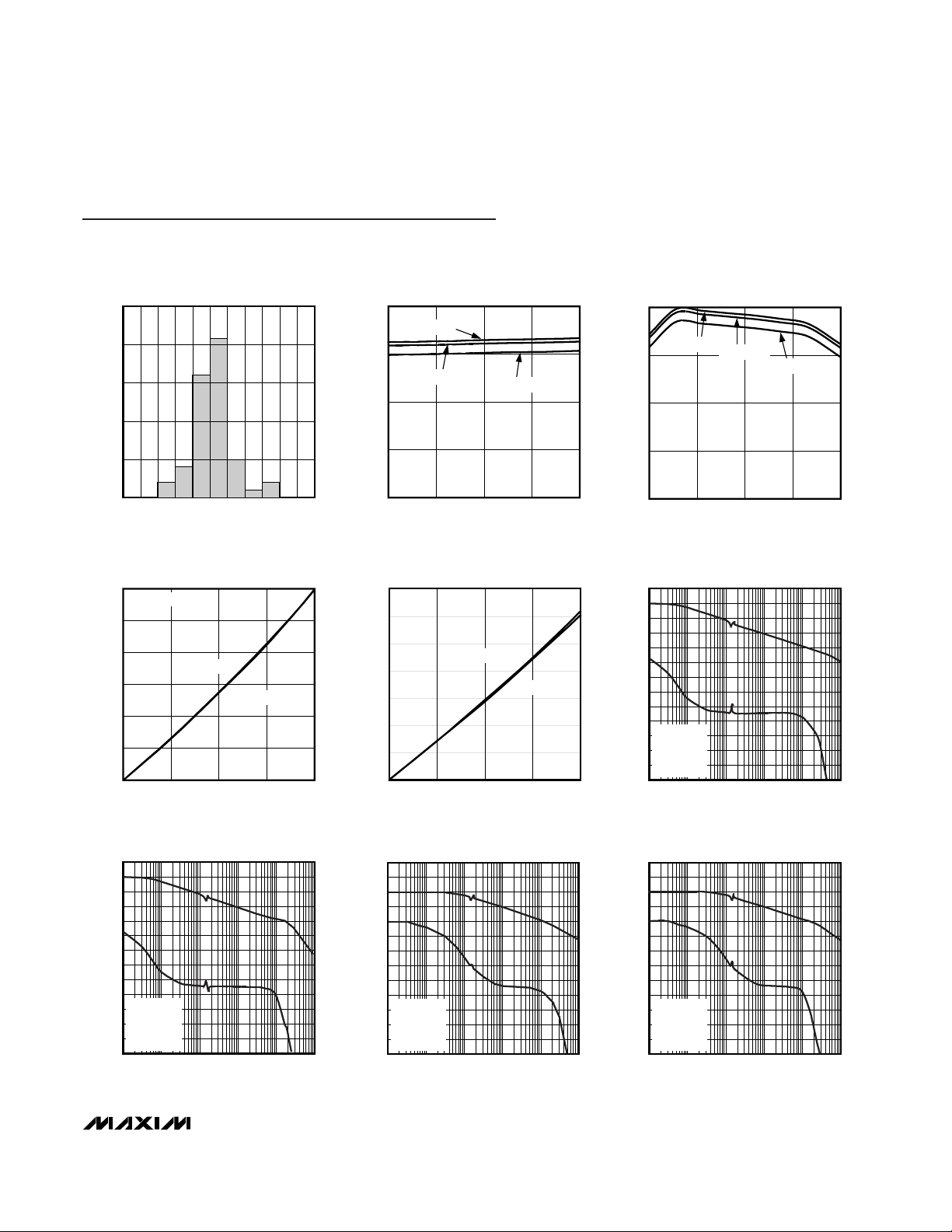
(VCC= 5V, VCM= 0V, RL= 10kΩ connected to VCC/2, SHDN = VCC, TA= +25°C, unless otherwise noted.)
MAX4238
GAIN AND PHASE vs. FREQUENCY
MAX4238/39 toc09
FREQUENCY (Hz)
GAIN AND PHASE (dB/DEGREES)
1M100k10k1k
-160
-140
-120
-100
-80
-60
-40
-20
0
20
40
60
80
-180
100 10M
VCC = 5V
GAIN = 40dB
R
L
= 10kΩ
C
L
= 68pF
MAX4238
GAIN AND PHASE vs. FREQUENCY
MAX4238/39 toc07
FREQUENCY (Hz)
GAIN AND PHASE (dB/DEGREES)
1M100k10k1k
-160
-140
-120
-100
-80
-60
-40
-20
0
20
40
60
80
-180
100 10M
VCC = 5V
GAIN = 60dB
R
L
= 10kΩ
C
L
= 100pF
MAX4238
GAIN AND PHASE vs. FREQUENCY
MAX4238/39 toc06
FREQUENCY (Hz)
GAIN AND PHASE (dB/DEGREES)
1M100k10k1k
-160
-140
-120
-100
-80
-60
-40
-20
0
20
40
60
80
-180
100 10M
VCC = 5V
GAIN = 60dB
R
L
= 10k
Ω
C
L
= 0pF
OUTPUT LOW VOLTAGE
vs. OUTPUT SINK CURRENT
MAX4238/39 toc05
SINK CURRENT (mA)
OUTPUT LOW VOLTAGE (V)
15105
0.05
0.10
0.15
0.20
0.25
0.35
0.30
0
020
VCC = 2.7V
VCC = 5V
OUTPUT HIGH VOLTAGE
vs. OUTPUT SOURCE CURRENT
MAX4238/39 toc04
SOURCE CURRENT (mA)
OUTPUT HIGH VOLTAGE (V)
15105
0.05
0.10
0.15
0.20
0.25
0.30
0
020
VOH = VCC - V
OUT
VCC = 2.7V
VCC = 5V
OFFSET VOLTAGE
vs. COMMON-MODE VOLTAGE
MAX4238/39 toc03
COMMON-MODE VOLTAGE (V)
OFFSET VOLTAGE (μV)
2.71.80.9
-0.2
0
0.2
0.4
-0.4
0 3.6
TA = +125°C
TA = +25°C
TA = -40°C
OFFSET VOLTAGE vs. SUPPLY VOLTAGE
MAX4238/39 toc02
SUPPLY VOLTAGE (V)
OFFSET VOLTAGE (μV)
4.84.13.4
-0.2
0
0.2
0.4
-0.4
2.7 5.5
TA = +125°C
TA = +25°C
TA = -40°C
INPUT OFFSET DISTRIBUTION
MAX4238/39 toc01
OFFSET VOLTAGE (μV)
PERCENTAGE OF UNITS (%)
1.51.20.90.60.30-0.3-0.6-0.9-1.2-1.5
10
20
30
40
50
0
MAX4238
GAIN AND PHASE vs. FREQUENCY
MAX4238/39 toc08
FREQUENCY (Hz)
GAIN AND PHASE (dB/DEGREES)
1M100k10k1k
-160
-140
-120
-100
-80
-60
-40
-20
0
20
40
60
80
-180
100 10M
VCC = 5V
GAIN = 40dB
R
L
= 10kΩ
C
L
= 0pF
Page 6
MAX4238/MAX4239
Ultra-Low Offset/Drift, Low-Noise,
Precision SOT23 Amplifiers
6 _______________________________________________________________________________________
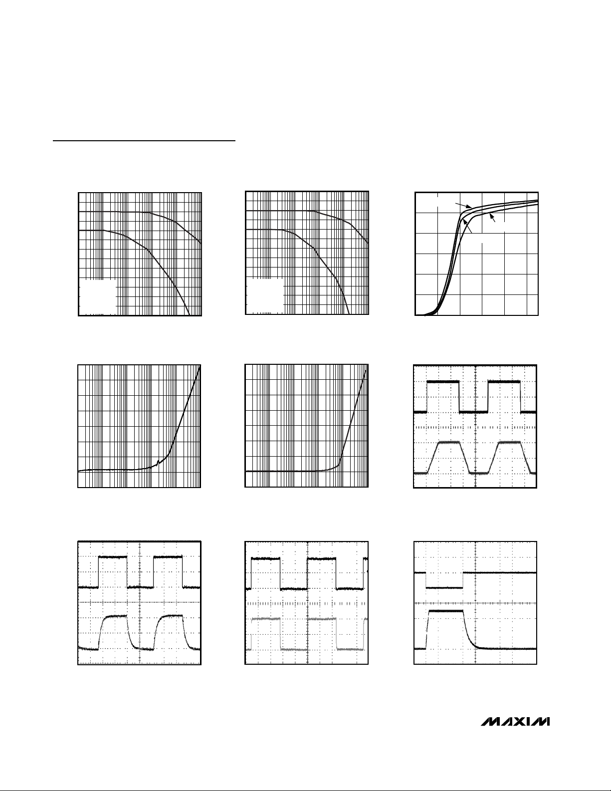
Typical Operating Characteristics (continued)
(VCC= 5V, VCM= 0V, RL= 10kΩ connected to VCC/2, SHDN = VCC, TA= +25°C, unless otherwise noted.)
COMMON-MODE REJECTION RATIO
vs. FREQUENCY
MAX4238/39 toc14
FREQUENCY (kHz)
CMRR (dB)
100100.1 1
-140
-120
-100
-80
-60
-40
-20
0
0.01 1000
-160
POWER-SUPPLY REJECTION RATIO
vs. FREQUENCY
MAX4238/39 toc13
FREQUENCY (kHz)
PSRR (dB)
100100.1 1
-140
-120
-100
-80
-60
-40
-20
0
-160
0.01 1000
MAX4239
GAIN AND PHASE vs. FREQUENCY
MAX4238/39 toc10
FREQUENCY (Hz)
GAIN AND PHASE (dB/DEGREES)
1E+61E+51E+41E+3
-160
-140
-120
-100
-80
-60
-40
-20
0
20
40
60
80
-180
1E+2 1E+7
VCC = 5V
GAIN = 40dB
R
L
= 10k
Ω
C
L
= 0pF
MAX4239
SMALL-SIGNAL TRANSIENT RESPONSE
MAX4238/39 toc17
AV = 10V/V
R
L
= 2kΩ
C
L
= 100pF
10μs/div
OUT
IN
500mV/div
50mV/div
MAX4238
LARGE-SIGNAL TRANSIENT RESPONSE
MAX4238/39 toc15
AV = 1V/V
R
L
= 2k
Ω
C
L
= 100pF
10μs/div
OUT
IN
1V/div
1V/div
MAX4239
GAIN AND PHASE vs. FREQUENCY
MAX4238/39 toc11
FREQUENCY (Hz)
GAIN AND PHASE (dB/DEGREES)
1E+61E+51E+41E+3
-160
-140
-120
-100
-80
-60
-40
-20
0
20
40
60
80
-180
1E+2 1E+7
VCC = 5V
GAIN = 40dB
R
L
= 10k
Ω
C
L
= 100pF
OVERVOLTAGE RECOVERY TIME
MAX4238/39 toc18
AV = 100V/V
R
L
= 10kΩ
V
CC
= 2.5V
V
EE
= -2.5V
400μs/div
0
0
OUT
IN
1V/div
50mV/div
MAX4238
SMALL-SIGNAL TRANSIENT RESPONSE
MAX4238/39 toc16
AV = 1V/V
R
L
= 2kΩ
C
L
= 100pF
10μs/div
OUT
50mV/div
IN
50mV/div
SUPPLY CURRENT vs. SUPPLY VOLTAGE
MAx4238/39 toc12
SUPPLY VOLTAGE (V)
SUPPLY CURRENT (μA)
4321
200
300
400
500
600
0
100
05
TA = +125°C
TA = +25°C
TA = -40°C
Page 7
Detailed Description
The MAX4238/MAX4239 are high-precision amplifiers
that have less than 2.5µV of input-referred offset and
low 1/f noise. These characteristics are achieved
through an autozeroing technique that samples and
cancels the input offset and noise of the amplifier. The
pseudorandom clock frequency varies from 10kHz to
15kHz, reducing intermodulation distortion present in
chopper-stabilized amplifiers.
Offset Error Sources
To achieve very low offset, several sources of error
common to autozero-type amplifiers need to be considered. The first contributor is the settling of the sampling
capacitor. This type of error is independent of inputsource impedance, or the size of the external gain-setting resistors. Maxim uses a design technique to avoid
large changes in the voltage on the sampling capacitor
to reduce settling time errors.
The second error contributor, which is present in both
autozero and chopper-type amplifiers, is the charge
injection from the switches. The charge injection
appears as current spikes at the input, and combined
with the impedance seen at the amplifier’s input, contributes to input offset voltage. Minimize this
feedthrough by reducing the size of the gain-setting
resistors and the input-source impedance. A capacitor
in parallel with the feedback resistor reduces the
amount of clock feedthrough to the output by limiting
the closed-loop bandwidth of the device.
The design of the MAX4238/MAX4239 minimizes the
effects of settling and charge injection to allow specification of an input offset voltage of 0.1µV (typ) and less
than 2.5µV over temperature (-40°C to +85°C).
1/f Noise
1/f noise, inherent in all semiconductor devices, is
inversely proportional to frequency. 1/f noise increases
3dB/octave and dominates amplifier noise at lower frequencies. This noise appears as a constantly changing
voltage in series with any signal being measured. The
MAX4238/MAX4239 treat 1/f noise as a slow varying
offset error, inherently canceling the 1/f noise.
MAX4238/MAX4239
Ultra-Low Offset/Drift, Low-Noise,
Precision SOT23 Amplifiers
_______________________________________________________________________________________ 7
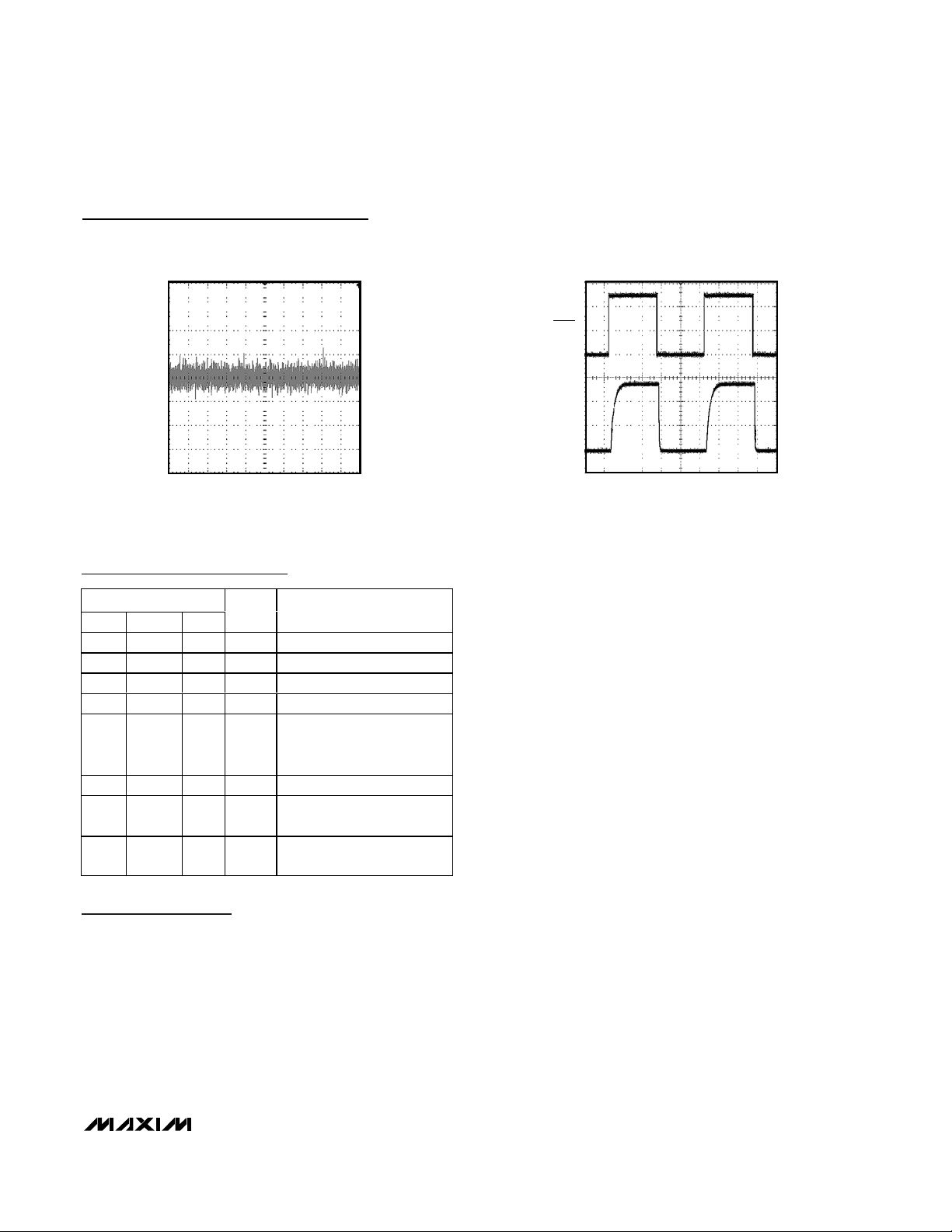
Typical Operating Characteristics (continued)
(VCC= 5V, VCM= 0V, RL= 10kΩ connected to VCC/2, SHDN = VCC, TA= +25°C, unless otherwise noted.)
SHUTDOWN WAVEFORM
MAX4238/39 toc20
RL = 10kΩ
C
L
= 100pF
10μs/div
OUT
2V/div
1V/div
SHDN
DC TO 10Hz NOISE
MAX4238/39 toc19
VCC = 2.5V
V
EE
= -2.5V
1s/div
OUT
2μV/div
PIN
TDFN
FUNCTION
116
Amplifier Output
224
Ground
333
Noninverting Input
4 4 2 IN- Inverting Input
551
Shutdown Input. Active-low
shutdown, connect to V
CC
for
normal operation.
667
Positive Power Supply
——
No Connection. Not internally
connected.
EP
—
EP
Exposed Pad. Connect EP to
GND.
Pin Description
SOT23 SO
NAME
OUT
GND
IN+
SHDN
V
5, 8 N.C.
—
CC
Page 8
MAX4238/MAX4239
Output Overload Recovery
Autozeroing amplifiers typically require a substantial
amount of time to recover from an output overload. This
is due to the time it takes for the null amplifier to correct
the main amplifier to a valid output. The MAX4238/
MAX4239 require only 3.3ms to recover from an output
overload (see Electrical Characteristics and Typical
Operating Characteristics).
Shutdown
The MAX4238/MAX4239 feature a low-power (0.1µA)
shutdown mode. When SHDN is pulled low, the clock
stops and the device output enters a high-impedance
state. Connect SHDN to V
CC
for normal operation.
Applications Information
Minimum and Maximum Gain
Configurations
The MAX4238 is a unity-gain stable amplifier with a gainbandwidth product (GBWP) of 1MHz. The MAX4239 is
decompensated for a GBWP of 6.5MHz and is stable with
a gain of 10V/V. Unlike conventional operational amplifiers, the MAX4238/MAX4239 have a maximum gain
specification. To maintain stability, set the gain of the
MAX4238 between AV= 1000V/V to 1V/V, and set the
gain of the MAX4239 between AV= 6700V/V and 10V/V.
ADC Buffer Amplifier
The low offset, fast settling time, and 1/f noise cancellation of the MAX4238/MAX4239 make these devices
ideal for ADC buffers. The MAX4238/MAX4239 are well
suited for low-speed, high-accuracy applications such
as strain gauges (see Typical Application Circuit).
Error Budget Example
When using the MAX4238/MAX4239 as an ADC buffer,
the temperature drift should be taken into account when
determining the maximum input signal. With a typical offset drift of 10nV/°C, the drift over a 10°C range is 100nV.
Setting this equal to 1/2LSB in a 16-bit system yields a
full-scale range of 13mV. With a single 2.7V supply, an
acceptable closed-loop gain is AV= 200. This provides
sufficient gain while maintaining headroom.
Ultra-Low Offset/Drift, Low-Noise,
Precision SOT23 Amplifiers
8 _______________________________________________________________________________________
OUT
N.C.GND
1
2
87N.C.
V
CC
IN-
IN+
SHDN
SO
TOP VIEW
3
4
6
5
MAX4238/
MAX4239
MAX4238/
MAX4239
GND
IN-IN+
16V
CC
5 SHDN
OUT
SOT23
2
34
MAX4238/
MAX4239
6
V
CC
5
SHDN4IN-
OUT
GND
IN+
1
EP*
23
TDFN
(3mm x 3mm x 0.8mm)
+
*CONNECT EP TO GND.
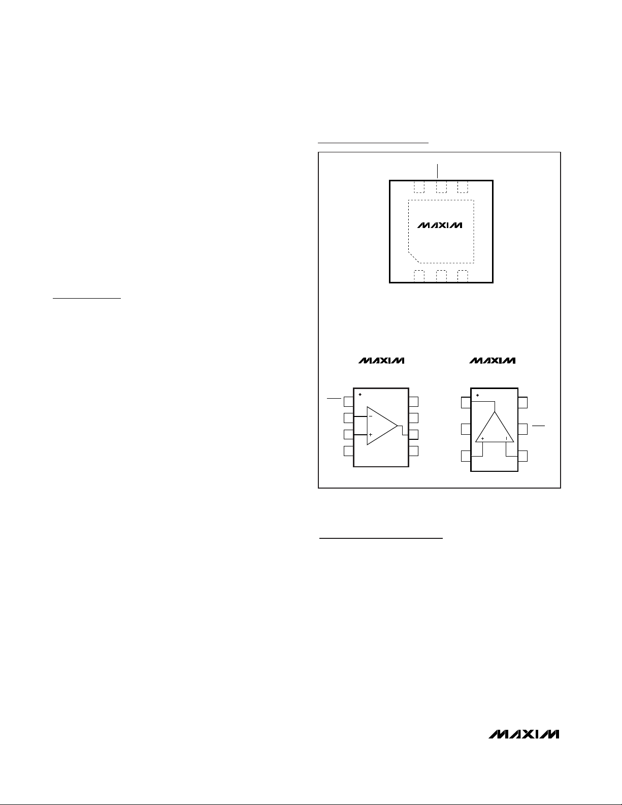
Pin Configurations
Chip Information
TRANSISTOR COUNT: 821
PROCESS: BiCMOS
Page 9
MAX4238/MAX4239
Ultra-Low Offset/Drift, Low-Noise,
Precision SOT23 Amplifiers
_______________________________________________________________________________________ 9
Package Information
(The package drawing(s) in this data sheet may not reflect the most current specifications. For the latest package outline information,
go to www.maxim-ic.com/packages
.)
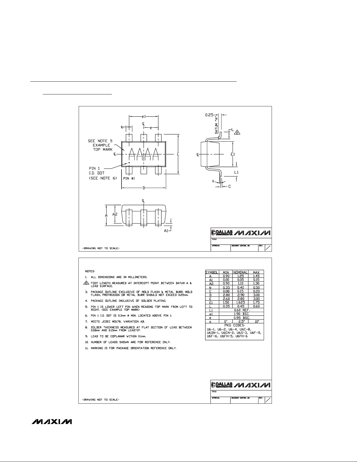
6LSOT.EPS
PACKAGE OUTLINE, SOT 6L BODY
21-0058
1
I
2
PACKAGE OUTLINE, SOT 6L BODY
21-0058
2
I
2
Page 10
MAX4238/MAX4239
Ultra-Low Offset/Drift, Low-Noise,
Precision SOT23 Amplifiers
10 ______________________________________________________________________________________
Package Information (continued)
(The package drawing(s) in this data sheet may not reflect the most current specifications. For the latest package outline information,
go to www.maxim-ic.com/packages
.)
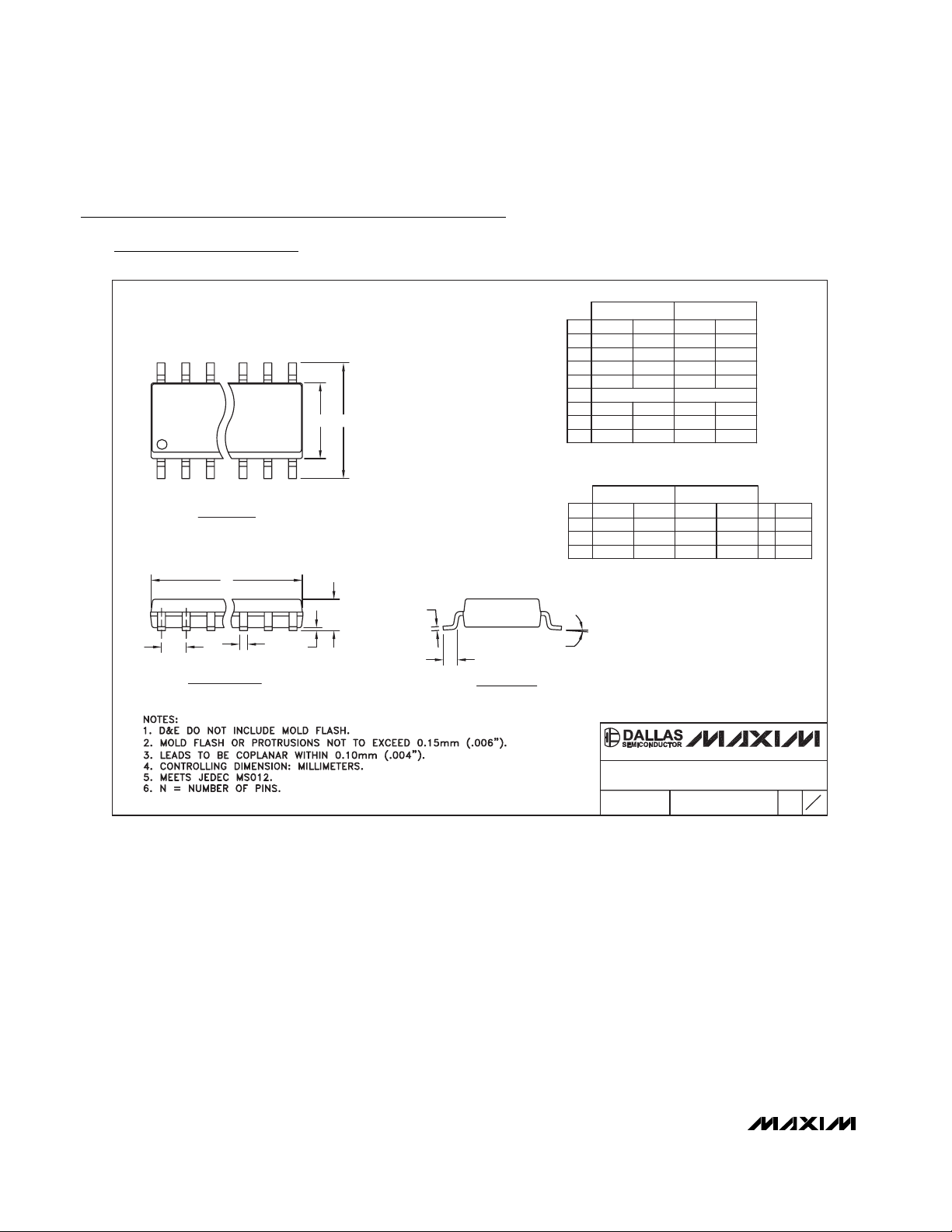
SOICN .EPS
PACKAGE OUTLINE, .150" SOIC
1
1
21-0041
B
REV.DOCUMENT CONTROL NO.APPROVAL
PROPRIETARY INFORMATION
TITLE:
TOP VIEW
FRONT VIEW
MAX
0.010
0.069
0.019
0.157
0.010
INCHES
0.150
0.007
E
C
DIM
0.014
0.004
B
A1
MIN
0.053A
0.19
3.80 4.00
0.25
MILLIMETERS
0.10
0.35
1.35
MIN
0.49
0.25
MAX
1.75
0.050
0.016L
0.40 1.27
0.3940.386D
D
MINDIM
D
INCHES
MAX
9.80 10.00
MILLIMETERS
MIN
MAX
16
AC
0.337 0.344 AB8.758.55 14
0.189 0.197 AA5.004.80 8
N MS012
N
SIDE VIEW
H 0.2440.228 5.80 6.20
e 0.050 BSC 1.27 BSC
C
HE
e
B
A1
A
D
0∞-8∞
L
1
VARIATIONS:
Page 11
MAX4238/MAX4239
Ultra-Low Offset/Drift, Low-Noise,
Precision SOT23 Amplifiers
Maxim cannot assume responsibility for use of any circuitry other than circuitry entirely embodied in a Maxim product. No circuit patent licenses are
implied. Maxim reserves the right to change the circuitry and specifications without notice at any time.
Maxim Integrated Products, 120 San Gabriel Drive, Sunnyvale, CA 94086 408-737-7600 ____________________ 11
© 2006 Maxim Integrated Products Printed USA is a registered trademark of Maxim Integrated Products, Inc.
Package Information (continued)
(The package drawing(s) in this data sheet may not reflect the most current specifications. For the latest package outline information,
go to www.maxim-ic.com/packages
.)
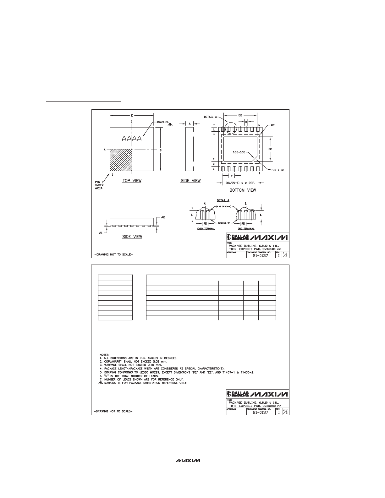
6, 8, &10L, DFN THIN.EPS
COMMON DIMENSIONS
SYMBOL MIN. MAX.
A 0.70 0.80
D 2.90 3.10
E 2.90 3.10
A1 0.00 0.05
L 0.20 0.40
PKG. CODE N D2 E2 e JEDEC SPEC b
[(N/2)-1] x e
PACKAGE VARIATIONS
0.25 MIN.k
A2 0.20 REF.
2.00 REF0.25±0.050.50 BSC2.30±0.1010T1033-1
2.40 REF0.20±0.05- - - - 0.40 BSC1.70±0.10 2.30±0.1014T1433-1
1.50±0.10 MO229 / WEED-3
0.40 BSC - - - - 0.20±0.05 2.40 REFT1433-2 14 2.30±0.101.70±0.10
T633-2 6 1.50±0.10 2.30±0.10 0.95 BSC MO229 / WEEA 0.40±0.05 1.90 REF
T833-2 8 1.50±0.10 2.30±0.10 0.65 BSC MO229 / WEEC 0.30±0.05 1.95 REF
T833-3 8 1.50±0.10 2.30±0.10 0.65 BSC MO229 / WEEC 0.30±0.05 1.95 REF
2.30±0.10 MO229 / WEED-3 2.00 REF0.25±0.050.50 BSC1.50±0.1010T1033-2
MAX4238/MAX4239 Package Code: T633-2
 Loading...