

Page 1
For free samples & the latest literature: http://www.maxim-ic.com, or phone 1-800-998-8800.
For small orders, phone 1-800-835-8769.
General Description
The MAX4194 is a variable-gain precision instrumentation amplifier that combines Rail-to-Rail®single-supply
operation, outstanding precision specifications, and a
high gain bandwidth. This amplifier is also offered in
three fixed-gain versions: the MAX4195 (G = +1V/V),
the MAX4196 (G = +10V/V), and the MAX4197 (G =
+100V/V). The fixed-gain instrumentation amplifiers feature a shutdown function that reduces the quiescent
current to 8µA. A traditional three operational amplifier
configuration is used to achieve maximum DC precision.
The MAX4194–MAX4197 have rail-to-rail outputs and
inputs that can swing to within 200mV of the negative rail
and to within 1.1V of the positive rail. All parts draw only
93µA and operate from a single +2.7V to +7.5V supply
or from dual ±1.35V to ±3.75V supplies. These amplifiers
are offered in 8-pin SO packages and are specified for
the extended temperature range (-40°C to +85°C).
See the MAX4198/MAX4199 data sheet for single-supply, precision differential amplifiers.
Applications
Medical Equipment
Thermocouple Amplifier
4–20mA Loop Transmitters
Data-Acquisition Systems
Battery-Powered/Portable Equipment
Transducer Interface
Bridge Amplifier
Features
♦ +2.7V Single-Supply Operation
♦ Low Power Consumption
93µA Supply Current
8µA Shutdown Current (MAX4195/96/97)
♦ High Common-Mode Rejection: 115dB (G = +10V/V)
♦ Low 50µV Input Offset Voltage (G ≥ +100V/V)
♦ Low ±0.01% Gain Error (G = +1V/V)
♦ 250kHz -3dB Bandwidth (G = +1V/V, MAX4194)
♦ Rail-to-Rail Outputs
MAX4194–MAX4197
Micropower, Single-Supply, Rail-to-Rail,
Precision Instrumentation Amplifiers
________________________________________________________________
Maxim Integrated Products
1
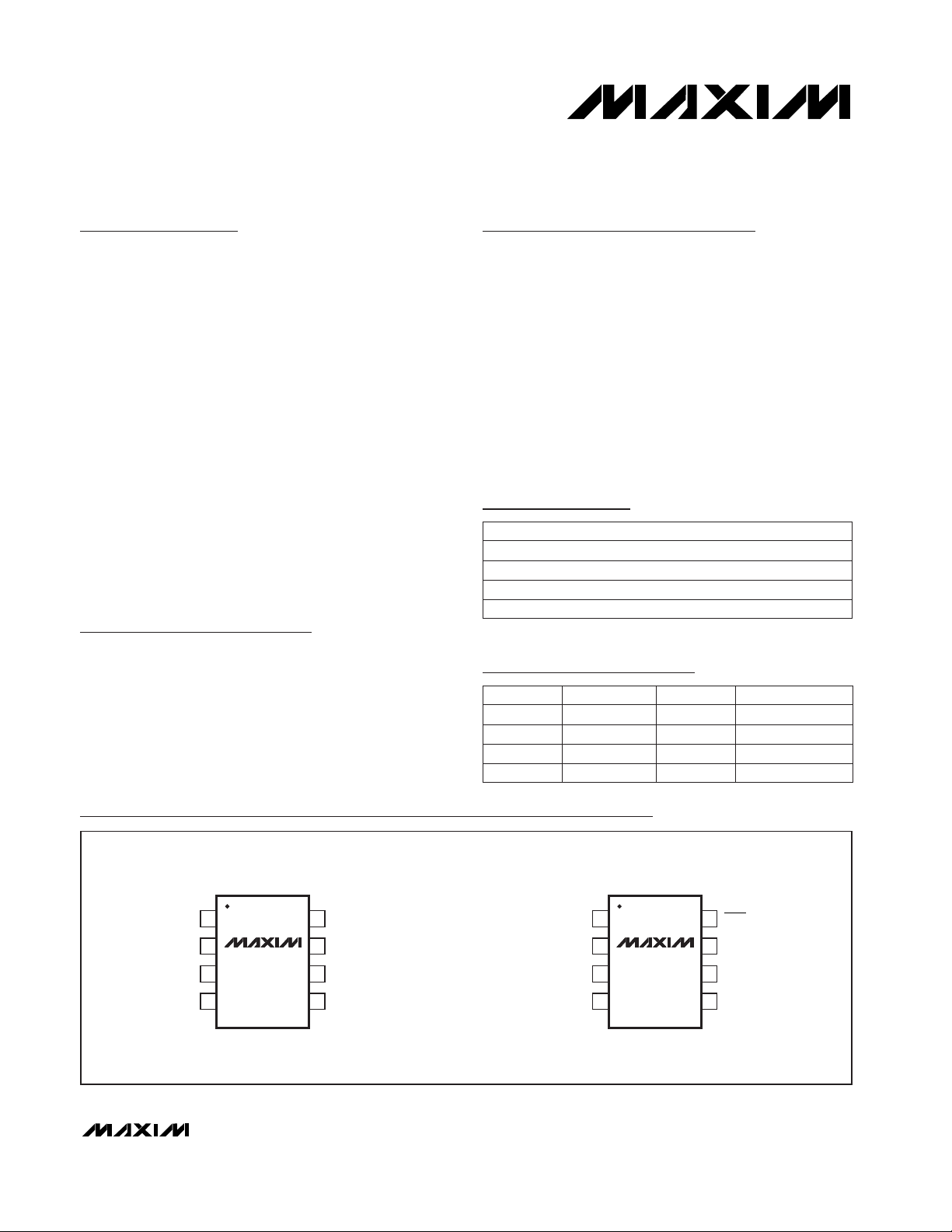
OUT
REFV
EE
1
2
87RG+
V
CC
IN-
IN+
RG-
SO
TOP VIEW
3
4
6
5
MAX4194
OUT
FBV
EE
1
2
87SHDN
V
CC
IN-
IN+
REF
SO
3
4
6
5
MAX4195
MAX4196
MAX4197
19-1468; Rev 0; 4/99
PART
MAX4194ESA
MAX4195ESA
MAX4196ESA
-40°C to +85°C
-40°C to +85°C
-40°C to +85°C
TEMP. RANGE PIN-PACKAGE
8 SO
8 SO
8 SO
Pin Configurations
Ordering Information
MAX4197ESA
-40°C to +85°C 8 SO
PART
MAX4194
MAX4195
MAX4196 Yes
Yes
No
SHUTDOWN GAIN (V/V)
Variable
+1
+10
MAX4197 Yes +100
Selector Guide
Rail-to-Rail is a registered trademark of Nippon Motorola, Ltd.
CMRR (dB)
95 (G = +1V/V)
95
115
115
Page 2
MAX4194–MAX4197
Micropower, Single-Supply, Rail-to-Rail,
Precision Instrumentation Amplifiers
2 _______________________________________________________________________________________
ABSOLUTE MAXIMUM RATINGS
ELECTRICAL CHARACTERISTICS
(VCC= +5V, VEE= 0, RL= 25kΩ tied to VCC/2, V
REF
= VCC/2, TA= T
MIN
to T
MAX
, unless otherwise noted. Typical values are at
T
A
= +25°C.)
Stresses beyond those listed under “Absolute Maximum Ratings” may cause permanent damage to the device. These are stress ratings only, and functional
operation of the device at these or any other conditions beyond those indicated in the operational sections of the specifications is not implied. Exposure to
absolute maximum rating conditions for extended periods may affect device reliability.
Supply Voltage (VCCto VEE)..................................................+8V
All Other Pins ..................................(VCC+ 0.3V) to (VEE- 0.3V)
Current into Any Pin..........................................................±30mA
Output Short-Circuit Duration (to VCCor VEE)........... Continuous
Continuous Power Dissipation (TA= +70°C)
SO (derate 5.9mW/°C above +70°C)........................... 471mW
Operating Temperature Range ...........................-40°C to +85°C
Junction Temperature......................................................+150°C
Storage Temperature Range.............................-65°C to +150°C
Lead Temperature (soldering, 10sec)............................ +300°C
I
SHDN
= VIL, MAX4195/96/97 only µA
Inferred by PSR
test
VCM= VEE+ 0.2V
to VCC- 1.1V,
f = 120Hz
VCM= VEE+ 0.2V
to VCC- 1.1V,
TA= T
MIN
to T
MAX
,
∆RS= 1kΩ
115
VCM= VCC/2
Differential
90 115
VCM= VEE+ 0.2V
to V
CC
- 1.1V,
T
A
= +25°C,
∆R
S
= 1kΩ
G = +1V/V
Common mode
VIN+ = VIN- = VCC/2, V
DIFF
= 0
G = +1V/V, VCM= VCC/2, TA= +25°C
Inferred from CMR test
VCM= VCC/2
CONDITIONS
106
101
dB
85
CMR
AC
AC Common-Mode Rejection
88 115
115
G = +1V/V
73 95
G = +10V/V
95 115
G = +100V/V
G = +1V/V
G = +10V/V
93 115
G = +100V/V
G = +1000V/V
dB
78 95
CMR
DC
DC Common-Mode Rejection
VVEE+ 0.2 VCC- 1.1V
IN
Input Voltage Range
Differential
1000
Common mode 4
812
I
SHDN
Shutdown Current
V
±1.35 ±3.75
pF
2.7 7.5
V
CC
Supply Voltage Range
1
MΩ
1000
R
IN
Input Resistance
C
IN
Input Capacitance
G = +1V/V
G = +10V/V
µV/°C
±1.0 ±4.0
TC
VOS
Input Offset Voltage Drift
(Note 1)
µA
93 110
I
CC
Quiescent Current
G = +100V/V
±100 ±450
G = +1000V/V
UNITSMIN TYP MAXSYMBOLPARAMETER
Single supply
Dual supplies
G ≥ +10V/V ±0.5 ±2.0
G = +10V/V, VCM= VCC/2, TA= +25°C
±75 ±225
G = +1000V/V, VCM= VCC/2, TA= +25°C
±50
G = +100V/V, VCM= VCC/2, TA= +25°C
±50 ±225
G = +10V/V, VCM= VCC/2, TA= T
MIN
to T
MAX
±75 ±345
G = +1V/V, VCM= VCC/2, TA= T
MIN
to T
MAX
G = +1000V/V, VCM= VCC/2, TA= T
MIN
to
µVV
OS
Input Offset Voltage
±50
G = +100V/V, VCM= VCC/2, TA= T
MIN
to
±50 ±345
±100 ±690
Page 3
MAX4194–MAX4197
Micropower, Single-Supply, Rail-to-Rail,
Precision Instrumentation Amplifiers
_______________________________________________________________________________________ 3
ELECTRICAL CHARACTERISTICS (continued)
(VCC= +5V, VEE= 0, RL= 25kΩ tied to VCC/2, V
REF
= VCC/2, TA= T
MIN
to T
MAX
, unless otherwise noted. Typical values are at
T
A
= +25°C.)
VCM= VCC/2
VCM= VCC/2
+2.7V ≤ VCC≤ +7.5V; VCM= +1.5V;
V
OUT
= +1.5V; V
REF
= +1.5V; RL= 25kΩ to
+1.5V; G = +1V/V, +10V/V, +100V/V
RL= 25kΩ to VCC/2
MAX4194 only
f = 0.1Hz to 10Hz
f = 10kHz
VCM= VCC/2
f = 10Hz
RL= 5kΩ to VCC/2
f = 100Hz
CONDITIONS
±0.01 ±0.1
1+ (50kΩ/RG)Gain Equation
mA±4.5I
SC
Short-Circuit Current (Note 2)
mV
100 200
VOH, V
OL
Output Voltage Swing
100 200
nA±1.0 ±3.0I
OS
Input Offset Current
pA/°C15TC
IB
dB90 120PSRPower-Supply Rejection
Input Bias Current Drift
30 100
30 100
pA
RMS
16
i
n
Input Noise Current
pA√Hz
0.1
pA/°C15TC
IOS
Input Offset Current Drift
85
2.4
0.76
UNITSMIN TYP MAXSYMBOLPARAMETER
f = 10Hz
75f = 100Hz
nV√Hz
72f = 10KHz
G = +1V/V
µV
RMS
1.4f = 0.1Hz to 10Hz
35f = 10Hz
32f = 100Hz
nV√Hz
31f = 10KHz
G = +10V/V
µV
RMS
0.7f = 0.1Hz to 10Hz
32f = 10Hz
31f = 100Hz
nV√Hz
8.7f = 10KHz
G = +100V/V
µV
RMS
0.6
e
n
Input Noise Voltage
f = 0.1Hz to 10Hz
VCC- V
OH
V
OL
VCC- V
OH
V
OL
G = +1V/V
G = +10V/V ±0.03 ±0.3
TA= +25°C,
VCM= VCC/2,
RL= 25kΩ,
VEE+ 0.1V ≤ V
OUT
≤ VCC- 0.1V
G = +1000V/V, MAX4194 ±0.5
G = +100V/V ±0.05 ±0.5
G = +10V/V ±0.03 ±0.3
TA= +25°C,
VCM= VCC/2,
RL= 5kΩ,
VEE+ 0.2V ≤ V
OUT
≤ VCC- 0.2V
G = +1000V/V, MAX4194
G = +1V/V
%
±0.5
Gain Error
G = +100V/V ±0.05 ±0.5
±0.01 ±0.1
VCM= VCC/2 nA620I
B
Input Bias Current
Page 4
MAX4194–MAX4197
Micropower, Single-Supply, Rail-to-Rail,
Precision Instrumentation Amplifiers
4 _______________________________________________________________________________________
Note 1: Guaranteed by design.
Note 2: Maximum output current (sinking/sourcing) in which the gain changes by less than 0.1%.
Note 3: This specification represents the typical temperature coefficient of an on-chip thin film resistor. In practice, the temperature
coefficient of the gain for the MAX4194 will be dominated by the temperature coefficient of the external gain-setting resistor.
ELECTRICAL CHARACTERISTICS (continued)
(VCC= +5V, VEE= 0, RL= 25kΩ tied to VCC/2, V
REF
= VCC/2, TA= T
MIN
to T
MAX
, unless otherwise noted. Typical values are at
T
A
= +25°C.)
V
SHDN
= VCC- 2.5V to VCC- 1.5V, G = +100V/V,
0.1%, V
OUT
= +3.5V
G = +1V/V, 0.1%, V
OUT
= +3.5V
MAX4196/MAX4197
G = +1V/V, 0.1%,
V
OUT
= +3.5V
MAX4194/MAX4195, G = +1V/V
G = +1V/V, 0.1%,
V
OUT
= +3V
VEE< V
SHDN
< V
CC
V
OUT
= 2Vp-p, G = +1V/V, f = 1kHz
V
OUT
= 2Vp-p, G = +1V/V
MAX4194
VEE+ 0.1V ≤ V
OUT
≤ VCC- 0.1V, VCM= VCC/2,
G = +1V/V, +10V/V, +100V/V, +1000V/V
0.1%, V
OUT
= 2Vp-p
CONDITIONS
ms0.5t
ON/OFF
On/Off Settling Time
ms1Power-Up Delay
ms0.5t
ENABLE
Enable Time From Shutdown
ms0.5t
SHDN
Time to Shutdown
µA±0.1
SHDN Input Current
VVCC- 2.5V
IL
Input Logic Voltage Low
VVCC- 1.5V
IH
Input Logic Voltage High
%0.001THDTotal Harmonic Distortion
ms
7
t
S
Settling Time
5
ppm/°C±16
ppm/°C
±1 ±15
±1 ±8
Gain Temperature Coefficient
(Note 1)
0.04
0.05
V/µs0.06SRSlew Rate
250
TC
50kΩ
50kΩ Resistance Temperature
Coefficient (Note 3)
%±0.001Nonlinearity
pF300C
L
Capacitive Load Stability
UNITSMIN TYP MAXSYMBOLPARAMETER
MAX4194
G = +1V/V
MAX4195 220
MAX4194
G = +10V/V
MAX4196
17
34
MAX4194 1.5
G = +100V/V
MAX4197
G = +1000V/V
V
OUT
≤ 0.1Vp-p,
VCM= VCC/2
MAX4194
kHz
3.1
0.147
BW-
3dB
-3dB Bandwidth
G = +1V/V
G = +10V/V
G = +100V/V
G = +1000V/V
MAX4195/MAX4196/
MAX4197 only
MAX4195/MAX4196/
MAX4197 only
MAX4195/MAX4196/
MAX4197 only
Page 5

MAX4194–MAX4197
Micropower, Single-Supply, Rail-to-Rail,
Precision Instrumentation Amplifiers
_______________________________________________________________________________________
5
100 1k 10k 100k 1M
MAX4194
SMALL-SIGNAL GAIN vs. FREQUENCY
MAX4194 toc01-1
FREQUENCY (Hz)
-6
-5
-4
-3
-2
-1
0
1
2
3
4
NORMALIZED GAIN (dB)
G = +100V/V
G = +10V/V
G = +1V/V
100 1k 10k 100k 1M
MAX4195/MAX4196/MAX4197
SMALL-SIGNAL GAIN vs. FREQUENCY
MAX4194 toc02-2
FREQUENCY (Hz)
G = +100V/V
G = +10V/V
G = +1V/V
-6
-5
-4
-3
-2
-1
0
1
2
3
4
NORMALIZED GAIN (dB)
11k10010
0.1% SETTLING TIME vs. GAIN
(V
OUT
= 2Vp-p)
10k
10
1
1k
100
MAX4194 toc03
GAIN (V/V)
SETTLING TIME (µs)
INPUT
(500mV/div)
OUTPUT
(500mV/div)
MAX4194
LARGE-SIGNAL PULSE RESPONSE
(GAIN = +1V/V)
MAX4194 toc04
20µs/div
INPUT
(50mV/div)
OUTPUT
(50mV/div)
MAX4194
SMALL-SIGNAL PULSE RESPONSE
(GAIN = +1V/V)
MAX4194 toc07
20µs/div
INPUT
(5mV/div)
OUTPUT
(500mV/div)
MAX4194
LARGE-SIGNAL PULSE RESPONSE
(GAIN = +100V/V)
MAX4194 toc05
200µs/div
INPUT
(5mV/div)
OUTPUT
(500mV/div)
MAX4197
LARGE-SIGNAL PULSE RESPONSE
(GAIN = +100V/V)
MAX4194 toc06
200µs/div
INPUT
(500µV/div)
OUTPUT
(50mV/div)
MAX4194
SMALL-SIGNAL PULSE RESPONSE
(GAIN = +100V/V)
MAX4194 toc08
200µs/div
INPUT
(500µV/div)
OUTPUT
(50mV/div)
MAX4197
SMALL-SIGNAL PULSE RESPONSE
(GAIN = +100V/V)
MAX4194 toc09
200µs/div
Typical Operating Characteristics
(VCC= +5V, VEE= 0, RL= 25kΩ tied to VCC/2, TA = +25°C, unless otherwise noted.)
Page 6

MAX4194–MAX4197
Micropower, Single-Supply, Rail-to-Rail,
Precision Instrumentation Amplifiers
6 _______________________________________________________________________________________
Typical Operating Characteristics (continued)
(VCC= +5V, VEE= 0, RL= 25kΩ tied to VCC/2, TA = +25°C, unless otherwise noted.)
0
-100
-120
-140
1 10 100 1k 10k 100k
POWER-SUPPLY REJECTION
vs. FREQUENCY
-80
MAX4194 toc10
FREQUENCY (Hz)
PSR (dB)
-60
-40
-20
G = +1V/V
G = +100V/V
G = +1000V/V
G = +10V/V
-30
-120
COMMON-MODE REJECTION
vs. FREQUENCY
-100
-110
MAX4194 toc11
FREQUENCY (Hz)
CMR (dB)
-80
-90
-70
-60
-50
-40
10 100 1k 10k 100k
G = +1V/V
G = +100V/V
G = +1,000V/V
G = +10V/V
1 10 100 1k 10k 100k
VOLTAGE-NOISE DENSITY
vs. FREQUENCY
MAX4194 toc12
FREQUENCY (Hz)
VOLTAGE NOISE DENSITY (nV/÷Hz)
1,000
1
10
100
G = +1V/V
G = +100V/V
G = +1000V/V
G = +10V/V
MAX4195/MAX4196
TOTAL HARMONIC DISTORTION PLUS NOISE
vs. FREQUENCY
MAX4194 toc13
THD + NOISE (%)
1.000
0
0.001
0.010
0.100
1 10 100 1k 10k
FREQUENCY (Hz)
G = +1V/V
MAX4195
MAX4196
G = +10V/V
84
86
90
88
94
96
92
98
-40
-15 10 35 60
85
SUPPLY CURRENT vs. TEMPERATURE
MAX4194 toc15
TEMPERATURE (°C)
SUPPLY CURRENT (µA)
G = +1000V/V
G = +1V/V, +10V/V
G = +100V/V
80
90
100
110
120
SUPPLY CURRENT vs. SUPPLY VOLTAGE
MAX4194 toc14
SUPPLY VOLTAGE (V)
SUPPLY CURRENT (µA)
25634 789
0
2
6
4
8
10
-40
-15 10 35 60
85
MAX4195/MAX4196/MAX4197
SHUTDOWN CURRENT vs. TEMPERATURE
MAX4194 toc16
TEMPERATURE (°C)
SHUTDOWN CURRENT (µA)
0
4
2
6
8
10
-40 10-15 35 60 85
INPUT BIAS CURRENT vs. TEMPERATURE
MAX4194TOC17
TEMPERATURE (°C)
INPUT BIAS CURRENT (nA)
Page 7

FUNCTION
MAX4194–MAX4197
Micropower, Single-Supply, Rail-to-Rail,
Precision Instrumentation Amplifiers
_______________________________________________________________________________________ 7
Pin Description
Typical Operating Characteristics (continued)
(VCC= +5V, VEE= 0, RL= 25kΩ tied to VCC/2, TA = +25°C, unless otherwise noted.)
-200
-100
-150
-50
0
50
-40 10-15 35 60 85
INPUT OFFSET CURRENT vs. TEMPERATURE
MAX4194TOC18
TEMPERATURE (°C)
INPUT OFFSET CURRENT (pA)
MAX4196
MAX4197
MAX4195
-100
-25
-50
-75
50
25
0
75
100
-40 10-15 35 60 85
INPUT OFFSET VOLTAGE vs. TEMPERATURE
MAX4194TOC19
TEMPERATURE (°C)
INPUT OFFSET VOLTAGE (µV)
MAX4197
MAX4196
MAX4195
MAX4194
(G = +10V/V)
MAX4194
(G = +100V/V,
G = +1000V/V)
Feedback. Connects to OUT.5—
Amplifier Output66
Positive Supply Voltage77
Shutdown Control8—
Negative Supply Voltage44
Noninverting Input33
Inverting Input22
Reference Voltage. Offsets output voltage.15
FB
OUT
V
CC
SHDN
V
EE
IN+
IN-
REF
1, 8 Connection for Gain Setting Resistor— RG-, RG+
MAX4194
FUNCTION
MAX4195
MAX4196
MAX4197
NAME
PIN
Page 8

Detailed Description
Input Stage
The MAX4194–MAX4197 family of low-power instrumentation amplifiers implements a three-amplifier topology (Figure 1). The input stage is composed of two
operational amplifiers that together provide a fixed-gain
differential and a unity common-mode gain. The output
stage is a conventional differential amplifier that provides an overall common-mode rejection of 115dB (G =
+10V/V). The MAX4194’s gain can be externally set
between +1V/V and +10,000V/V (Table 1). The
MAX4195/MAX4196/MAX4197 have on-chip gain-setting resistors (Figure 2), and their gains are fixed at
+1V/V, +10V/V, and +100V/V, respectively.
Input Voltage Range
and Detailed Operation
The common-mode input range for all of these amplifiers is VEE+ 0.2V to VCC- 1.1V. Ideally, the instrumentation amplifier (Figure 3) responds only to a differential
voltage applied to its inputs, IN+ and IN-. If both inputs
are at the same voltage, the output is V
REF
. A differen-
tial voltage at IN+ (V
IN+
) and IN- (V
IN-
) develops an
identical voltage across the gain-setting resistor, causing a current (IG) to flow. This current also flows
through the feedback resistors of the two input amplifiers A1 and A2, generating a differential voltage of:
V
OUT2
- V
OUT1
= IG · (R1+ RG+ R1)
where V
OUT1
and V
OUT2
are the output voltages of A1
and A2, RGis the gain-setting resistor (internal or external to the part), and R1 is the feedback resistor of the
input amplifiers.
IGis determined by the following equation:
IG= (V
IN+
- V
IN-
) / R
G
The output voltage (V
OUT
) for the instrumentation
amplifier is expressed in the following equation:
V
OUT
= (V
IN+
- V
IN-
) · [(2 · R1) / RG] + 1
The common-mode input range is a function of the
amplifier’s output voltage and the supply voltage. With
a power supply of VCC, the largest output signal swing
can be obtained with REF tied to VCC/2. This results in
an output voltage swing of ±VCC/2. An output voltage
swing less than full-scale increases the common-mode
input range.
MAX4194–MAX4197
Micropower, Single-Supply, Rail-to-Rail,
Precision Instrumentation Amplifiers
8 _______________________________________________________________________________________
R1*
R
1
*
R
2
*
R
2
*
R
2
*
R
2
*
V
IN-
REF
OUT
R
G
**
I
G
I
G
V
IN+
V
OUT2
V
OUT1
V
OUT2
- V
OUT1
V
IN+
- V
IN-
A1
A2
A3
V
OUT
= (V
IN+
- V
IN-
) · (1 +
)
2R1
R
G
* R1 = R2 = 25kΩ
** R
G
= INTERNAL TO MAX4195/MAX4196/MAX4197
R
G
= EXTERNAL TO MAX4194
Figure 3. Instrumentation Amplifier Configuration
25k
25k
25k
25k
25k
25k
IN-
RG-
OUT
REF
V
EE
V
CC
IN+
RG+
MAX4194
Figure 1. MAX4194 Simplified Block Diagram
25k
25k
25k
25k
25k
25k
IN-
SHDN
OUT
REF
V
CC
V
EE
FB
R
G
IN+
MAX4195
MAX4196
MAX4197
Figure 2. MAX4195/MAX4196/MAX4197 Simplified Block
Diagram
Page 9

MAX4194–MAX4197
Micropower, Single-Supply, Rail-to-Rail,
Precision Instrumentation Amplifiers
_______________________________________________________________________________________ 9
V
CM
vs. V
OUT
Characterization
Figure 4 illustrates the MAX4194 typical common-mode
input voltage range over output voltage swing at unitygain (pins 1 and 8 left floating), with a single-supply
voltage of VCC= +5V and a bias reference voltage of
V
REF
= VCC/2 = +2.5V. Points A and D show the full
input voltage range of the input amplifiers (VEE+ 0.2V
to VCC- 1.1V) since, with +2.5V output, there is zero
input differential swing. The other points (B, C, E, and
F) are determined by the input voltage range of the
input amps minus the differential input amplitude necessary to produce the associated V
OUT
. For the higher
gain configurations, the VCMrange will increase at the
endpoints (B, C, E, and F) since a smaller differential
voltage is necessary for the given output voltage.
Rail-to-Rail Output Stage
The MAX4194–MAX4197’s output stage incorporates a
common-source structure that maximizes the dynamic
range of the instrumentation amplifier.
The output can drive up to a 25kΩ (tied to VCC/2) resistive load and still typically swing within 30mV of the
rails. With an output load of 5kΩ tied to VCC/2, the output voltage swings within 100mV of the rails.
Shutdown Mode
The MAX4195–MAX4197 feature a low-power shutdown
mode. When the shutdown pin (SHDN) is pulled low,
the internal amplifiers are switched off and the supply
current drops to 8µA typically (Figures 5a, 5b, and 5c).
This disables the instrumentation amplifier and puts its
output in a high-impedance state. Pulling SHDN high
enables the instrumentation amplifier.
Applications Information
Setting the Gain (MAX4194)
The MAX4194’s gain is set by connecting a single,
external gain resistor between the two RG pins (pin 1
and pin 8), and can be described as:
G = 1 + 50kΩ / R
G
where G is the instrumentation amplifier’s gain and R
G
is the gain-setting resistor.
The 50kΩ resistor of the gain equation is the sum of the
two resistors internally connected to the feedback loops
of the IN+ and IN- amplifiers. These embedded feedback resistors are laser trimmed, and their accuracy
and temperature coefficients are included in the gain
and drift specification for the MAX4194.
0
1
3
2
4
5
021 345
OUTPUT VOLTAGE (V)
COMMON-MODE INPUT VOLTAGE (V)
B
C
0.03 4.97
D
A
F
E
MAX4194/MAX4195
G = +1V/V
REF = +2.5V/+1.5V
V
CC
= +5V/+3V
V
EE
= 0
T
A
= +25°C
Figure 4. Common-Mode Input Voltage vs. Output Voltage
Figure 5a. MAX4195 Shutdown Mode
*
Leave pins 1 and 8 open for G = +1V/V.
GAIN (V/V)
CLOSEST RG (1%)
(Ω)
CLOSEST RG(5%)
(Ω)
+1 ∞ * ∞ *
+2 49.9k 51k
+5 12.4k 12k
+10 5.62k 5.6k
+20 2.61k 2.7k
+50 1.02k 1.0k
+100 511 510
+200 249 240
+500 100 100
+1,000 49.9 51
+2,000 24.9 24
+5,000 10 10
+10,000 4.99 5.1
Table 1. MAX4194 External Gain Resistor
Selection
50µs/div
MAX4195
OUT
AC-COUPLED
= 2V,
(V
DIFF
G = +1V/V)
(500mV/div)
SHDN
(5V/div)
Page 10

The accuracy and temperature drift of the RGresistors
also influence the IC’s precision and gain drift, and can
be derived from the equation above. With low RGvalues, which are required for high-gain operation, parasitic resistances may significantly increase the gain
error.
Capacitive Load Stability
The MAX4194–MAX4197 are stable for capacitive loads
up to 300pF (Figure 6a). Applications that require
greater capacitive-load driving capability can use an
isolation resistor (Figure 6b) between the output and
the capacitive load to reduce ringing on the output signal. However, this alternative reduces gain accuracy
because R
ISO
(Figure 6c) forms a potential divider with
the load resistor.
MAX4194–MAX4197
Micropower, Single-Supply, Rail-to-Rail,
Precision Instrumentation Amplifiers
10 ______________________________________________________________________________________
INPUT
(50mV/div)
OUTPUT
(50mV/div)
50µs/div
Figure 6b. Small-Signal Pulse Response with Excessive
Capacitive Load (R
L
= 25kΩ, CL= 1000pF)
INPUT
(50mV/div)
OUTPUT
(50mV/div)
50µs/div
Figure 6c. Small-Signal Pulse Response with Excessive
Capacitive Load and Isolating Resistor (R
ISO
= 75Ω, RL=
25k
Ω
, CL= 1000pF)
IN-
(MAX4194)
(INTERNAL, MAX4195)
V
EE
V
REF
V
REF
V
OUT
V
CC
R
ISO
R
L
C
L
IN+
R
G
= ∞
Figure 6a. Using a Resistor to Isolate a Capacitive Load from
the Instrumentation Amplifier (G = +1V/V)
SHDN
(5V/div)
MAX4196
OUT
AC-COUPLED
(V
DIFF
= 200mV,
G = +10V/V)
(500mV/div)
50µs/div
Figure 5c. MAX4197 Shutdown Mode
Figure 5b. MAX4196 Shutdown Mode
MAX4197
OUT
AC-COUPLED
= 20mV,
(V
DIFF
G = +100V/V)
(500mV/div)
SHDN
(5V/div)
50µs/div
Page 11

MAX4194–MAX4197
Micropower, Single-Supply, Rail-to-Rail,
Precision Instrumentation Amplifiers
______________________________________________________________________________________ 11
Power-Supply Bypassing and Layout
Good layout technique optimizes performance by
decreasing the amount of stray capacitance at the
instrumentation amplifier’s gain-setting pins. Excess
capacitance will produce peaking in the amplifier’s frequency response. To decrease stray capacitance, minimize trace lengths by placing external components as
close to the instrumentation amplifier as possible. For
best performance, bypass each power supply to
ground with a separate 0.1µF capacitor.
Transducer Applications
The MAX4194–MAX4197 instrumentation amplifiers can
be used in various signal-conditioning circuits for thermocouples, PT100s, strain gauges (displacement sensors), piezoresistive transducers (PRTs), flow sensors,
and bioelectrical applications. Figure 7 shows a simplified example of how to attach four strain gauges (two
identical two-element strain gauges) to the inputs of the
MAX4194. The bridge contains four resistors, two of
which increase and two of which decrease by the same
ratio.
With a fully balanced bridge, points A (IN+) and B (IN-)
see half the excitation voltage (V
BRIDGE
). The low
impedance (120Ω to 350Ω) of the strain gauges, however, could cause significant voltage drop contributions
by the wires leading to the bridge, which would cause
excitation variations. Output voltage V
OUT
can be cal-
culated as follows:
V
OUT
= VAB· G
where G = (1 + 50kΩ / RG) is the gain of the instrumentation amplifier.
Since VABis directly proportional to the excitation, gain
errors may occur.
Figure 7. Strain Gauge Connection to the MAX4194
IN-
V
EE
V
CC
V
AB
= V
IN+
- V
IN-
V
BRIDGE
R
R
R
R
R
G
IN+
RG+
RG-
OUT
REFERENCE
µP
REF
B
A
MAX144
ADC
R = 120Ω - 350Ω
___________________Chip Information
TRANSISTOR COUNT: 432
Page 12

MAX4194–MAX4197
Micropower, Single-Supply, Rail-to-Rail,
Precision Instrumentation Amplifiers
Maxim cannot assume responsibility for use of any circuitry other than circuitry entirely embodied in a Maxim product. No circuit patent licenses are
implied. Maxim reserves the right to change the circuitry and specifications without notice at any time.
12
____________________Maxim Integrated Products, 120 San Gabriel Drive, Sunnyvale, CA 94086 408-737-7600
© 1999 Maxim Integrated Products Printed USA is a registered trademark of Maxim Integrated Products.
SOICN.EPS
Package Information
 Loading...